JETWAY JNF711-2807 User manual

Technical Manual
Of
Intel Bay Trail Series CPU
Based
SBC
NO.G03-NF711-F
Revision: 1.0
Release date: January 8, 2018
Trademark:
* Specifications and Information contained in this documentation are furnished for information use only, and are
subject to change at any time without notice, and should not be construed as a commitment by manufacturer.

ii
Environmental Protection Announcement
Do not dispose this electronic device into the trash while discarding. To minimize
pollution and ensure environment protection of mother earth, please recycle.

iii
ENVIRONMENTAL SAFETY INSTRUCTION ....................................................................... iv
USER’S NOTICE .................................................................................................................. v
MANUAL REVISION INFORMATION ................................................................................... v
ITEM CHECKLIST ................................................................................................................ v
CHAPTER 1 INTRODUCTION OF THE MOTHERBOARD
1-1 FEATURE OF MOTHERBOARD ............................................................................ 1
1-2 SPECIFICATION .................................................................................................... 2
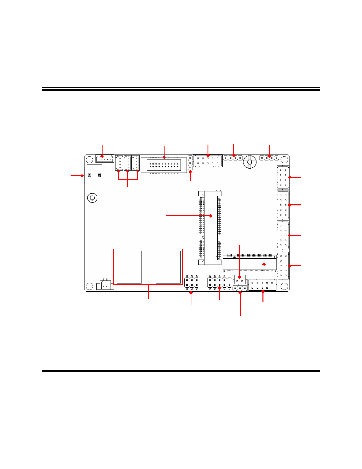
1-3 LAYOUT DIAGRAM ............................................................................................... 3
CHAPTER 2 HARDWARE INSTALLATION
2-1 JUMPER SETTING................................................................................................. 6
2-2 CONNECTORS, WAFERS AND HEADERS ........................................................... 9
CHAPTER 3 INTRODUCING BIOS
3-1 ENTERING SETUP................................................................................................. 15
3-2 BIOS MENU SCREEN ............................................................................................ 16
3-3 FUNCTION KEYS................................................................................................... 17
3-4 GETTING HELP...................................................................................................... 17
3-5 MEMU BARS.......................................................................................................... 18
3-6 MAIN MENU ........................................................................................................... 19
3-7 ADVANCED MENU ................................................................................................ 20
3-8 CHIPSET MENU..................................................................................................... 30
3-9 SECURITY MENU .................................................................................................. 33
3-10 BOOT MENU.......................................................................................................... 34
3-11 SAVE & EXIT MENU .............................................................................................. 35
TABLE OF CONTENT

iv
Environmental Safety Instruction
Avoid the dusty, humidity and temperature extremes. Do not place the product in
any area where it may become wet.
0 to 60 centigrade is the suitable temperature. (The figure comes from the request
of the main chipset)
Generally speaking, dramatic changes in temperature may lead to contact
malfunction and crackles due to constant thermal expansion and contraction from
the welding spots’ that connect components and PCB. Computer should go
through an adaptive phase before it boots when it is moved from a cold
environment to a warmer one to avoid condensation phenomenon. These water
drops attached on PCB or the surface of the components can bring about
phenomena as minor as computer instability resulted from corrosion and oxidation
from components and PCB or as major as short circuit that can burn the
components. Suggest starting the computer until the temperature goes up.
The increasing temperature of the capacitor may decrease the life of computer.
Using the close case may decrease the life of other device because the higher
temperature in the inner of the case.
Attention to the heat sink when you over-clocking. The higher temperature may
decrease the life of the device and burned the capacitor.

v
USER’S NOTICE
COPYRIGHT OF THIS MANUAL BELONGS TO THE MANUFACTURER. NO PART OF THIS MANUAL,
INCLUDING THE PRODUCTS AND SOFTWARE DESCRIBED IN IT MAY BE REPRODUCED, TRANSMITTED
OR TRANSLATED INTO ANY LANGUAGE IN ANY FORM OR BY ANY MEANS WITHOUT WRITTEN
PERMISSION OF THE MANUFACTURER.
THIS MANUAL CONTAINS ALL INFORMATION REQUIRED TO USE THIS MOTHER-BOARD SERIES AND WE
DO ASSURE THIS MANUAL MEETS USER’S REQUIREMENT BUT WILL CHANGE, CORRECT ANY TIME
WITHOUT NOTICE. MANUFACTURER PROVIDES THIS MANUAL “AS IS” WITHOUT WARRANTY OF ANY
KIND, AND WILL NOT BE LIABLE FOR ANY INDIRECT, SPECIAL, INCIDENTIAL OR CONSEQUENTIAL
DAMAGES (INCLUDING DAMANGES FOR LOSS OF PROFIT, LOSS OF BUSINESS, LOSS OF USE OF DATA,
INTERRUPTION OF BUSINESS AND THE LIKE).
PRODUCTS AND CORPORATE NAMES APPEARING IN THIS MANUAL MAY OR MAY NOT BE
REGISTERED TRADEMARKS OR COPYRIGHTS OF THEIR RESPECTIVE COMPANIES, AND THEY ARE
USED ONLY FOR IDENTIFICATION OR EXPLANATION AND TO THE OWNER’S BENEFIT, WITHOUT
INTENT TO INFRINGE.
Manual Revision Information
Reversion Revision History Date
1.0 First Edition January 8, 2018
Item Checklist
Motherboard
User’s Manual
CD for motherboard utilities
Cable(s)

1
Chapter 1
Introduction of the Motherboard
1-1 Feature of Motherboard
Onboard Intel® Bay Trail Series Processor, with low power consumption never
denies high performance
1* 5V DC-IN power
Onboard 2GB DDR3L DRAM
Onboard 1* full-size Mini-PCIE/MSATA slot
Onboard 1* M.2 slot (M key, SATA interface, 2242)
Support 1* Intel gigabit Ethernet LAN
Support VGA and eDP pin header and dual display output
1 * Internal USB3.0 & 3 * Internal USB2.0
2 * Internal COM port
Compliance with ErP standard
Support Watchdog function
Solution for IoT, Machine control & Intelligent Home

2
1-2 Specification
Spec Description
Design PCB size: 1.8’’ (84 mm x 55 mm)
Embedded CPU Integrated with Intel® Bay Trail series CPU (TDP: 4.3W/6W)
Memory Onboard 2G un-buffered DRAM
Expansion Slot 1 * full-size Mini-PCIE/MSATA shared slot
Storage 1 * full-size Mini-PCIE/MSATA shared slot
1 * M.2 SATA slot (M key, SATA interface, 2242)
LAN Chip
Integrated with Intel PCI-E Gigabit LAN chip
Support Fast Ethernet LAN function of providing
10/100/1000Mbps Ethernet data transfer rate
Audio Chip Realtek ALC662 HD Audio Codec integrated
Audio driver and utility included
BIOS AMI Flash ROM
Internal I/O
1* 2-pin internal 5V DC -in power connector
1* 5-pin USB 3.0 wafer (Expansible to 1* USB 3.0 port)
3* 4-pin USB 2.0 wafer (Expansible to 3* USB 2.0 ports)
1* eDP port wafer
1* VGA port wafer
1* SMBUS header
1* LAN_LED header
1* LAN wafer
1* GPIO wafer
2* Serial port wafer (COM1/2, COM1 supports RS232/422/485
function)
1* Front panel audio wafer
1* Buzzer wafer
1* Front panel header

3
1-3 Layout Diagram
Internal Diagram-Front Side:
USB 3.0
Wafer
USB 2.0
Wafers
eDP Port
Wafer
VGA Port
Wafer
SMBUS
Header
LAN_LED
Header
5V DC-in
Power Connector
Front Panel
Header
LAN
Wafer
GPIO
Wafer
COM1
Serial Port
Wafer
Front Panel
Audio
Wafer
COM2
Serial Port
Wafer
Full
-
size
Mini-PCIE/MSATA Slot
(
MPEST
)
M.2
SATA
Slot
(
M.2
)
AT_MODE
JBAT
LCD_VDD
Buzzer
Wafer
Onboard DRAM

4
Internal Diagram-Back Side:
*Note: CPU is the most important part of the board and very fragile to any possible harm. Make sure
that there is no damage to the CPU during any installation procedures!
Intel CPU
Onboard DRAM

5
Connectors, Wafers & Headers
P/N Name Description
DCIN Internal 5V DC–in power connector 2-pin Block
USB30 USB 3.0 port wafer 5-pin Block
USB20/21/22 USB 2.0 port wafer X3 4-pin Block
eDP Embedded display port wafer 20-pin Block
VGA VGA port wafer 10-pin Block
SMBUS SMBUS header 4-pin Block
LAN_LED LAN activity LED Header 4-pin Block
LAN LAN wafer 8-pin Block
FP_AUDIO Front panel audio wafer 9-pin Block
GPIO GPIO wafer 10-pin Block
COM1 RS232/422/485 serial port wafer 9-pin Block
COM2 RS232 serial port wafer 9-pin Block
BUZZ Buzzer wafer 4-pin Block
JW_FP
Front panel header(PWR LED/ HD
D
LED/Power Button /Reset)
9-pin Block

6
Jumper
Jumper Name Description
JBAT Pin (1-2): Clear CMOS RAM Settings
Pin (3-4): Reset RTC
Pin (5-6): Flash Descriptors Override
6-Pin Block
AT_MODE AT/ATX Mode Select 3-Pin Block
LCD_VDD eDP Port LCD VDD Select 3-Pin Block
Chapter 2
Hardware Installation
2-1 Jumper Setting
Pin 1&2 of JBAT (6-pin): Clear CMOS RAM Setting
1-2 Closed: Clear CMOS(One Touch).
1-2 Open: Normal(Default);
Pin 1
2
Pin (1&2) of JBAT
→
Clear CMOS
2
Pin 1
JBAT

7
Pin 3&4 of JBAT (6-pin): Reset RTC Select
Pin 1
2
2
Pin 1
Pin (3&4) of JBAT
→
Reset RTC
3-4 Open: Normal;
3-4 Closed: Reset RTC.
Pin 5&6 of JBAT (6-pin): Flash Deacriptors Override Select
Pin 1
2
2
Pin 1
Pin (5&6) of JBAT
→
Flash Override
5-6 Open:Enable Security Measures
in the Flash Descriptor(Default);
5-6 Closed: Disable Security Measures
in the Flash Descriptor(Override).
JBAT
JBAT

8
AT_MODE (3-pin): AT Mode /ATX Mode Select
AT_MODE
→
AT/ATX Mode Select
1
3
1-2 Closed: ATX Mode Select(Defualt);
;
2-3 Closed: AT Mode Select.
1
3
*ATX Mode Selected: Press power button to power on after power input ready;
AT Mode Selected: Directly power on as power input ready.
LCD_VDD (3-pin): eDP LCD VDD Select
1-2 Closed: LCD VDD 3.3V Select;
;
3
1
3
1
LCD_VDD
→
LCD VDD Select
1-2 Closed: LCD VDD 5V Select.
;
LCD_VDD
AT_MODE

9
2-2 Connectors, Wafers and Headers
(1) DCIN(2-pin) : Internal 5V DC-in power connector
Pin No. Definition
1 5V
2 GND
Pin1
(2) USB30 (5-pin): USB 3.0 Port Wafer
Pin 1
TX_P
TX_N
GND
RX_P
RX_N
DCIN
USB30

10
(3) USB20/ USB21/ USB22 (4-pin): USB 2.0 Port Wafer
Pin 1
GND
VCC
DATA-
DATA+
(4) EDP (20-pin): EDP Wafer
Pin1
2
19
20
Pin NO. Pin Define Pin NO. Pin Define
Pin 1 LCD_VDD Pin 2 GND
Pin 3 LCD_VDD Pin 4 DATA1_N
Pin 5 GND Pin 6 DATA1_P
Pin 7 GND Pin 8 GND
Pin 9 *LCD_BKLT Pin 10 DATA0_N
Pin 11 *LCD_BKLT Pin 12 DATA0_P
Pin 13 NC Pin 14 GND
Pin 15 EDP_HPD Pin 16 AUX_P
Pin 17 *BKLT_EN Pin 18 AUX_N
Pin 19 *BKLT_CTL Pin 20 GND
*Note: 1. LCD_BKLT backlight power is 5V default and 1A maximum.
2. BKLT_EN / BKLT_CTL is 3.3V level.
USB20
USB21
USB22
EDP

11
(5) VGA (10-pin): VGA Wafer
Pin 1
HSYNC
DDC_SCL
GND
DDC_SDA
GND
VSYNC
RED
GND
BLUE
2
GREEN
(6) SMBUS (4-pin): SMBUS Header
Pin 1
NC
SMB_SCL
GND
SMB_SDA
(7) LAN_LED (4-pin): LAN Activity LED Header
Pin 1
VCC
ACT_LED_N
1G_LED_N
100M_LED_N
VGA
SMBUS
LAN_LED

12
(8) LAN (8-pin): LAN Wafer
MDI_1_P
Pin 1
MDI_1_N
MDI_2_P
MDI_2_N
MDI_0_P
MDI_0_N
MDI_3_P
MDI_3_N
2
(9) GPIO (10-pin): GPIO Wafer
VCC
GPIO
3
GND
GPIO6
GPIO7
GPIO
2
GPIO5
Pin 1
GPIO4
2
GPIO
1
GPIO0
(10) FP_AUDIO (9-pin): Line-Out, MIC-In Wafer
This header connects to Front Panel Line-out, MIC-In connector with cable.
LINEOUT_JD
GND
MIC_R
MIC_JD
Pin 1
LINEOUT_R
2
GND
MIC_L
JD_SENSE
LINEOUT_L
LAN
GPIO
FP_
AUDIO

13
(11) JW_FP (9-pin): Front Panel Header
Pin 1
HDLED+
PWRBTN
PWRLED+
HDLED
-
RESET
GND
VCC
2
GND
PWRLED-
(12) BUZZ(2-pin): Buzzer Wafer
Pin 1
BUZZER_N
BUZZER_P
JW_FP
BUZZ

14
(13) COM1/2 (9-pin): Serial Port Wafers
COM1
:
RS232/422/485 Serial Port Wafer;
COM2
:
RS232 Serial Port Wafer.
COM1: RS232/422/485
Serial Port
Pin 1
2
Pin 1
2
COM2:
RS232 Serial Port
*Notice: RS422, RS485 function is supported by COM1 wafer only, with compatible
COM cable for RS422 or RS 485 function. User also needs to go to BIOS to set
‘Transmission Mode Select’ for COM1 (refer to Page 21).
Pin NO. RS232 *RS422 *RS485
Pin 1 DCD TX- DATA-
Pin 2 RXD TX+ DATA+
Pin 3 TXD RX+ NC
Pin 4 DTR RX- NC
Pin 5 GNG GND GND
Pin 6 DSR NC NC
Pin 7 RTS NC NC
Pin 8 CTS NC NC
Pin 9 RI NC NC
COM1
COM2

15
Chapter 3
Introducing BIOS
Notice! The BIOS options in this manual are for reference only. Different
configurations may lead to difference in BIOS screen and BIOS
screens in manuals are usually the first BIOS version when the board is
released and may be different from your purchased motherboard.
Users are welcome to download the latest BIOS version form our
official website.
The BIOS is a program located on a Flash Memory on the motherboard. This program
is a bridge between motherboard and operating system. When you start the computer,
the BIOS program will gain control. The BIOS first operates an auto-diagnostic test
called POST (power on self test) for all the necessary hardware, it detects the entire
hardware device and configures the parameters of the hardware synchronization.
Only when these tasks are completed done it gives up control of the computer to
operating system (OS). Since the BIOS is the only channel for hardware and software
to communicate, it is the key factor for system stability, and in ensuring that your
system performance as its best.
3-1 Entering Setup
Power on the computer and by pressing <Del> immediately allows you to enter Setup.
If the message disappears before your respond and you still wish to enter Setup,
restart the system to try again by turning it OFF then ON or pressing the “RESET”
button on the system case. You may also restart by simultaneously pressing <Ctrl>,
<Alt> and <Delete> keys. If you do not press the keys at the correct time and the
system does not boot, an error message will be displayed and you will again be asked
to
Press <Del> to enter Setup
Table of contents
Other JETWAY Motherboard manuals

JETWAY
JETWAY I401R5A User manual

JETWAY
JETWAY 845DBA3A User manual

JETWAY
JETWAY MI215 Series User manual

JETWAY
JETWAY JNP891 Series User manual

JETWAY
JETWAY 754TURBOR208 User manual

JETWAY
JETWAY A76M Series User manual

JETWAY
JETWAY 993BSR4A User manual

JETWAY
JETWAY P4XFCR2A User manual

JETWAY
JETWAY V4MDMPR3A User manual

JETWAY
JETWAY NC97 User manual

JETWAY
JETWAY NF835F Series User manual

JETWAY
JETWAY 845GDAR1A User manual

JETWAY
JETWAY 618TAS3A User manual

JETWAY
JETWAY NF796M-H310 Series User manual

JETWAY
JETWAY NMF691 Series User manual

JETWAY
JETWAY S755MAX User manual

JETWAY
JETWAY 815EDA1A User manual

JETWAY
JETWAY P4MDMR7A User manual

JETWAY
JETWAY LA0H Series User manual

JETWAY
JETWAY NU95 Series User manual