JETWAY NC7A Series User manual

NC7A Series User Manual
NO. G03-NC7A-F
Revision: 1.0
Release date: July 31, 2017
Trademark:
* Specifications and Information contained in this documentation are furnished for information use only, and are
subject to change at any time without notice, and should not be construed as a commitment by manufacturer.

i
Environmental Protection Announcement
Do not dispose this electronic device into the trash while discarding. To minimize
pollution and ensure environment protection of mother earth, please recycle.

ii
ENVIRONMENTAL SAFETY INSTRUCTION...........................................................................iii
USER’S NOTICE .......................................................................................................................iv
MANUAL REVISION INFORMATION.......................................................................................iv
ITEM CHECKLIST.....................................................................................................................iv
CHAPTER 1 INTRODUCTION
1-1 PRODUCT FEATURES...............................................................................................1
1-2 SPECIFICATION.........................................................................................................2
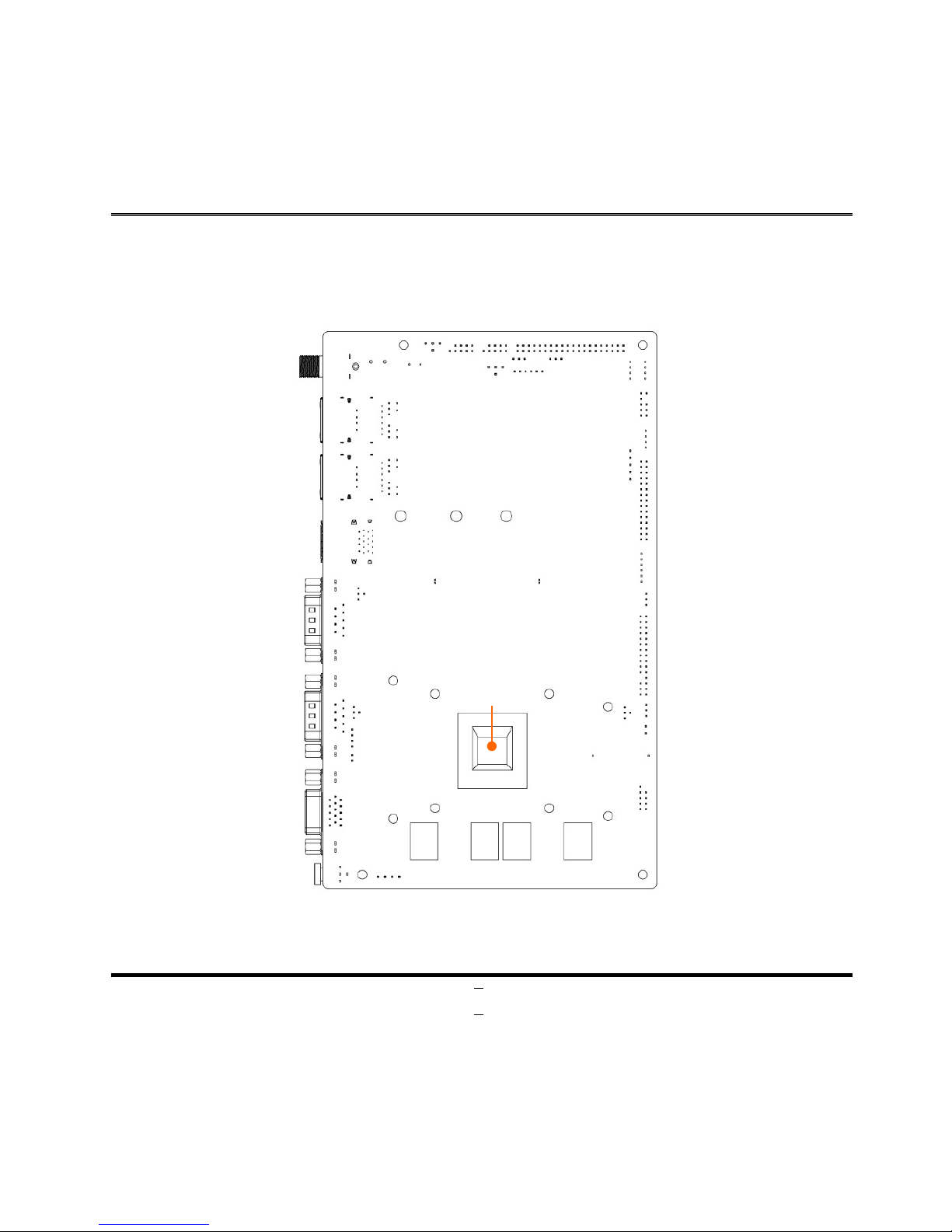
1-3 MAIN BOARD DIAGRAM ...........................................................................................3
CHAPTER 2 HARDWARE INSTALLATION
2-1 LOCATION OF INTERNAL JUMPER AND CONNECTOR .......................................5
2-2 INTERNAL JUMPER AND CONNECTOR SETTING.................................................6
2-2-1 CONNECTORS .............................................................................................10
2-2-2 HEADERS .....................................................................................................11
CHAPTER 3 INTRODUCING BIOS
3-1 ENTERING SETUP .....................................................................................................19
3-2 BIOS MENU SCREEN ................................................................................................20
3-3 FUNCTION KEYS .......................................................................................................20
3-4 GETTING HELP ..........................................................................................................21
3-5 MEMU BARS...............................................................................................................21
3-6 MAIN MENU................................................................................................................21
3-7 ADVANCED MENU.....................................................................................................23
3-8 CHIPSET MENU..........................................................................................................33
3-9 SECURITY MENU.......................................................................................................35
3-9 BOOT MENU...............................................................................................................36
3-11 SAVE & EXIT MENU...................................................................................................37
TABLE OF CONTENT

iii
Environmental Safety Instruction
Avoid the dusty, humidity and temperature extremes. Do not place the product in
any area where it may become wet.
0 to 60 centigrade is the suitable temperature. (The figure comes from the request
of the main chipset)
Generally speaking, dramatic changes in temperature may lead to contact
malfunction and crackles due to constant thermal expansion and contraction from
the welding spots’ that connect components and PCB. Computer should go
through an adaptive phase before it boots when it is moved from a cold
environment to a warmer one to avoid condensation phenomenon. These water
drops attached on PCB or the surface of the components can bring about
phenomena as minor as computer instability resulted from corrosion and oxidation
from components and PCB or as major as short circuit that can burn the
components. Suggest starting the computer until the temperature goes up.
The increasing temperature of the capacitor may decrease the life of computer.
Using the close case may decrease the life of other device because the higher
temperature in the inner of the case.
Attention to the heat sink when you over-clocking. The higher temperature may
decrease the life of the device and burned the capacitor.

iv
USER’S NOTICE
COPYRIGHT OF THIS MANUAL BELONGS TO THE MANUFACTURER. NO PART OF THIS MANUAL,
INCLUDING THE PRODUCTS AND SOFTWARE DESCRIBED IN IT MAY BE REPRODUCED, TRANSMITTED
OR TRANSLATED INTO ANY LANGUAGE IN ANY FORM OR BY ANY MEANS WITHOUT WRITTEN
PERMISSION OF THE MANUFACTURER.
THIS MANUAL CONTAINS ALL INFORMATION REQUIRED TO USE THIS MOTHER-BOARD SERIES AND WE
DO ASSURE THIS MANUAL MEETS USER’S REQUIREMENT BUT WILL CHANGE, CORRECT ANY TIME
WITHOUT NOTICE. MANUFACTURER PROVIDES THIS MANUAL “AS IS” WITHOUT WARRANTY OF ANY
KIND, AND WILL NOT BE LIABLE FOR ANY INDIRECT, SPECIAL, INCIDENTAL OR CONSEQUENTIAL
DAMAGES (INCLUDING DAMAGES FOR LOSS OF PROFIT, LOSS OF BUSINESS, LOSS OF USE OF DATA,
INTERRUPTION OF BUSINESS AND THE LIKE).
PRODUCTS AND CORPORATE NAMES APPEARING IN THIS MANUAL MAY OR MAY NOT BE
REGISTERED TRADEMARKS OR COPYRIGHTS OF THEIR RESPECTIVE COMPANIES, AND THEY ARE
USED ONLY FOR IDENTIFICATION OR EXPLANATION AND TO THE OWNER’S BENEFIT, WITHOUT
INTENT TO INFRINGE.
Manual Revision Information
Reversion Revision History Date
1.0 First Edition July 31, 2017
Item Checklist
Motherboard
DVD for motherboard utilities
User’s Manual
Cable(s)
I/O Back panel shield

1
Chapter 1: Introduction
1-1 Product Features
Intel® Celeron™ J1900 (2.0 GHz) quad-core processor
Support DirectX 11 3D Graphics Acceleration
Onboard SAMSUNG 4G/1333MHz DDR3L Memory
Support up to 2 Displays, LVDS,EDP, VGA
1 x SATA3 6Gb/s Port
1 x MINI PCI-E Socket
1 x M.2 Socket (2242/2260/2280)
Dual Intel® Gigabit LAN
4 x Serial Ports (COM1/2 RS232/422/485), 8-bit GPIO
2 x USB 3.0 Ports, 6 * USB 2.0 Ports, Watchdog Timer
9 ~ 28V DC-in or 4-pin Internal Power Connector
5.25” Form Factor (120mm * 200mm)

2
1-2 Specification
Spec
Description
CPU
Intel®Celeron™ J1900 (2.0 GHz) quad-core processor
Memory
Onboard SAMSUNG 4G/1333MHz DDR3L up to 8GB
Expansion Slot
1* Full-size Mini PCIe slot
1* M.2 (2242/2260/2280)
1* SIM Card Holder
Storage
1* SATA III 6G/s Connector
LAN Chip
2* Intel® i211AT GbE
Support Fast Ethernet LAN function of providing
10/100/1000Mbps Ethernet data transfer rate
Audio Chip
Realtek ALC662 dual channel HD Audio Codec integrated
Audio driver and utility included
BIOS
AMI 64MB Flash ROM
Rear I/O
1 * VGA
2* RJ45, 10/100/1000 Mbps
2* USB3.0, 2* USB2.0 ports
2* RS232/422/485 ports with 5V/12V selectable header
1* DC-in, 1* Power Button
Internal I/O
2* USB 2.0 header
1* PS/2 header
1* LVDS, 1* eDP
2* RS-232 with 5V/12V selectable header
1* SATA III 6G/s Connector
1* Full-size Mini PCIe
1* M.2 (2242/2260/2280)
1* GPIO (4 in/4 out)
1* Chassis intrusion, 1* Audio Header, 1* SMBUS/I2C
1* AT_ATX Mode header
1* Support Expansion card(2* COM+2* USB2.0)

3
1-3 Main Board Diagram: Front
Power Button
VGA
USB3.0 Ports
COM1
COM2
Top:
RJ-45
LAN Port1
Middle/Bottom:
USB2.0 Port
Top:
RJ-45
LAN Port2
Middle/Bottom:
USB2.0 Port
DC-in
Connector
CPUFAN Header
Mini PCIe
Connector
SIM Card Socket
SATA3 Connector
JW_FP Header
EDP1 Header
INVERTER1 Header
JP3 Header
M.2 Connector
SPEAK_CON2 Header
F_USB1 Header
F_USB2Header
DCIN3 Connector F_PH1 Connector
PS2_CON1 Header
COM3 COM4
LVDS1 Header
SMBUS Header
FP_AUDIO Header

4
Main Board Diagram: Back
Intel CPU

5
Chapter 2
Hardware Installation
2-1 Location of Internal Jumper and Connector
Power Button
VGA
USB3.0 Ports
COM1
COM2
Top:
RJ-45
LAN Port1
Middle/Bottom:
USB2.0 Port
Top:
RJ-45
LAN Port2
Middle/Bottom:
USB2.0 Port
DC-in
Connector
CPUFAN Header
Mini PCIe
Connector
SIM Card Socket
SATA3 Connector
JW_FP Header
EDP1 Header
INVERTER1 Header
JP3 Header
M.2 Connector
SPEAK_CON2 Header
F_USB1 Header
F_USB2 Header
DCIN3 Connector
COPEN
JP1
JP2
JBAT1
JPLED
JPLCD
AT_MODE
JPCOM4
JP4
JPCOM3
JPCOM2
JPCOM1
I2C
JP5
LVDS1 Header
SMBUS Header
FP_AUDIO Header
F_PH1 Connector
PS2_CON1 Header
COM3 COM4

6
2-2 Internal Jumper and Connector Setting
(1) JP1 (3-pin): eDP Backlight VCC 5V /12V Select
1
1-2 Closed:
5V (Default);
3
1
3
2-3 Closed:
12V.
(2) JP2 (4-pin): eDP LCD VCC 3.3V / 5V /12V Select
4-6 Closed:
12V.
3-4 Closed:
5V;
2-4 Closed:
3.3V (Default);
3
6
4
2
3
6
4
2
3
6
4
2

7
(3) JBAT1 (4-pin): Clear CMOS Setting
4-6 Closed:
RTC_RST.
2-4 Closed:
CLEAR CMOS;
3-4 Closed:
(Default);
3
2
4
6
3
2
4
6
3
2
4
6
(4) JPLED (3-pin): LVDS Backlight VCC 5V / 12V Select
1
1-2 Closed:
5V (Default);
3
1
3
2-3 Closed:
12V.

8
(5) JPLCD (4-pin): LVDS LCD VCC 3.3V / 5V /12V Select
4-6 Closed:
12V.
3-4 Closed:
5V;
2-4 Closed:
3.3V (Default);
3
2
4
6
3
2
4
6
3
2
4
6
(6) AT_Mode (3-pin): AT/ATX Mode Function Select
AT Mode.
Pin1
2-3 Closed:
ATX Mode (default);
1-2 Closed:
*ATX Mode Selected: Press power button to power on after power input ready;
AT Mode Selected: Directly power on as power input ready.
(7) JP4 (3-pin): PS2 5VSB / VCC Select
VCC.
Pin1
2-3 Closed:
5VSB (default);
1-2 Closed:

9
(8) JPCOM1/2/3/4 (4-pin): COM1/COM2/COM3/COM4 5V /12V Select
4-6 Closed:
12V.
3-4 Closed:
5V;
2-4 Closed:
RING (Default);
3
2
4
6
3
2
4
6
3
2
4
6
4-6 Closed:
12V.
3-4 Closed:
5V;
2-4 Closed:
RING (Default);
3
2
4
6
3
2
4
6
3
2
4
6

10
2-2-1 Connectors
(1) Rear I/O Connectors
Icon Name Function
Power Button Press to turn on/off the system.
VGA Port T
o connect display device that support VGA
specification.
COM Port Mainly for user to connect external MODEM
or other
devices that supports Serial Communications Interface.
USB 3.0 Port To
connect USB keyboard, mouse or other devices
compatible with USB specification.
USB 3.0 ports
supports up to 5Gbps data transfer rate.
RJ-45 LAN Port This connector is standard RJ-45 LAN jack
for Network
connection.
USB 2.0 Port To
connect USB keyboard, mouse or other devices
compatible with USB specification.
DC-in Power Jack
Connector For user to connect compatible power adapter to provide
power supply for the system.
COM1
Power Button USB 3.0 Port
RJ-45
LAN2 Port
RJ-45
LAN1 Port
COM2
USB 2.0 Port
VGA
DC-in

11
2-2-2 Headers
(1) CPUFAN (4-pin): CPUFAN Header
(2) JW_FP (9-pin): Front Panel Header
VCC
HLED-
GND
FP_RST-
VSB_LED
PWRLED
GND
FP_SPSW
HLED+
PIN 1
2

12
(3) COPEN (2-PIN): Case Open Message Display Function
1
2
COPEN-
GND
Pin 1-2 Close:When Case open function pin short to GND, the Case open function
was detected. When Used, needs to enter BIOS and enable ‘Case Open Detect’
function. In this case if your case is removed, next time when you restart your
computer, a message will be displayed on screen to inform you of this.
(4) EDP1 (30-pin): eDP Header
Pin 29
Pin30
Pin1
Pin2

13
Pin NO.
Pin Define
Pin NO.
Pin Define
Pin 1
BKLT_PW
Pin 2
EDP_INVCC
Pin 3
BKLT_PW
Pin 4
GND
Pin 5
GND
Pin 6
NC
Pin 7
NC
Pin 8
NC
Pin 9
EDP_LCD_VCC
Pin 10
NC
Pin 11
EDP_LCD_VCC
Pin 12
EDP_BKLTCTL
Pin 13
GND
Pin 14
GND
Pin 15
EDP_BKLTEN
Pin 16
EDP_AUXP_C
Pin 17
EDP_HPD
Pin 18
EDP_AUXN_C
Pin 19
GND
Pin 20
GND
Pin 21
EDP_LAN+3
Pin 22
EDP_LANE-3
Pin 23
EDP_LAN+2
Pin 24
EDP_LANE-2
Pin 25
GND
Pin 26
GND
Pin 27
EDP_LAN+1
Pin 28
EDP_LANE-1
Pin 29
EDP_LAN+0
Pin 30
EDP_LANE-0
(5) INVERTER1 (6-Pin): LVDS1 Inverter Header

14
(6) JP3 (2-Pin): Brightness Setting Header
-
BRTNSS_UP
+
BRTNSS_DN
(7) LVDS1 (30-Pin): 24-bit dual channel LVDS Header
Pin 2
Pin 1
Pin NO.
Pin Define
Pin NO.
Pin Define
Pin 1
LVD_VCC
Pin 2
LVD_VCC
Pin 3
LVD_VCC
Pin 4
LVDS_PRSNT#
Pin 5
GND
Pin 6
GND
Pin 7
LVDSA_DATAN0
Pin 8
LVDSA_DATAP0

15
Pin 9
LVDSA_DATAN1
Pin 10
LVDSA_DATAP1
Pin 11
LVDSA_DATAN2
Pin 12
LVDSA_DATAP2
Pin 13
GND
Pin 14
GND
Pin 15
LVDSA_CLKN
Pin 16
LVDSA_CLKP
Pin 17
LVDSA_DATAN3
Pin 18
LVDSA_DATAP3
Pin 19
LVDSB_DATAN0
Pin 20
LVDSB_DATAP0
Pin 21
LVDSB_DATAN1
Pin 22
LVDSB_DATAP1
Pin 23
LVDSB_DATAN2
Pin 24
LVDSB_DATAP2
Pin 25
GND
Pin 26
GND
Pin 27
LVDSB_CLKN
Pin 28
LVDSB_CLKP
Pin 29
LVDSB_DATAN3
Pin 30
LVDSB_DATAP3
*Note: LVDS is optional by customized order.
(8) SMBUS (5-pin): SMBUS Function Header
Pin 1
SCL
SDA
SMBALERT-
GND
VCC3
(9) SPEAK_CON2 (4-pin): Speaker Header
Table of contents
Other JETWAY Motherboard manuals

JETWAY
JETWAY G03-7F2WE-F User manual

JETWAY
JETWAY TIH77MG7 User manual

JETWAY
JETWAY NF93 Series User manual

JETWAY
JETWAY NU591S User manual

JETWAY
JETWAY P4X400DBR3A User manual

JETWAY
JETWAY P4XDMR1A User manual

JETWAY
JETWAY S447R3A User manual

JETWAY
JETWAY 917GBAR3A User manual

JETWAY
JETWAY G03-NF795-F User manual

JETWAY
JETWAY JBC390F841VGU User manual

JETWAY
JETWAY G03-NF9D-F User manual

JETWAY
JETWAY V400DA1A User manual

JETWAY
JETWAY P4MBMS - REV 1.0 User manual

JETWAY
JETWAY NC9T User manual

JETWAY
JETWAY NF796-Q370 User manual

JETWAY
JETWAY NLBT-I1900 Series User manual

JETWAY
JETWAY I406R1A User manual

JETWAY
JETWAY 845GPR2A User manual

JETWAY
JETWAY NP591 User manual

JETWAY
JETWAY 865GFTR3A User manual