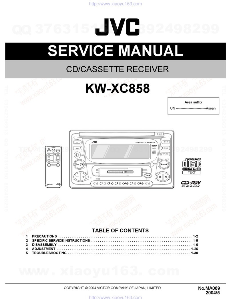
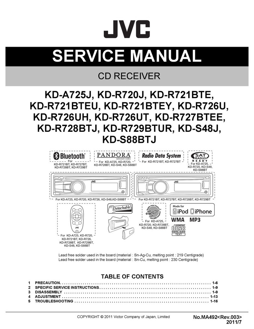
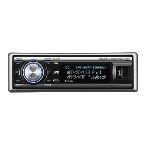
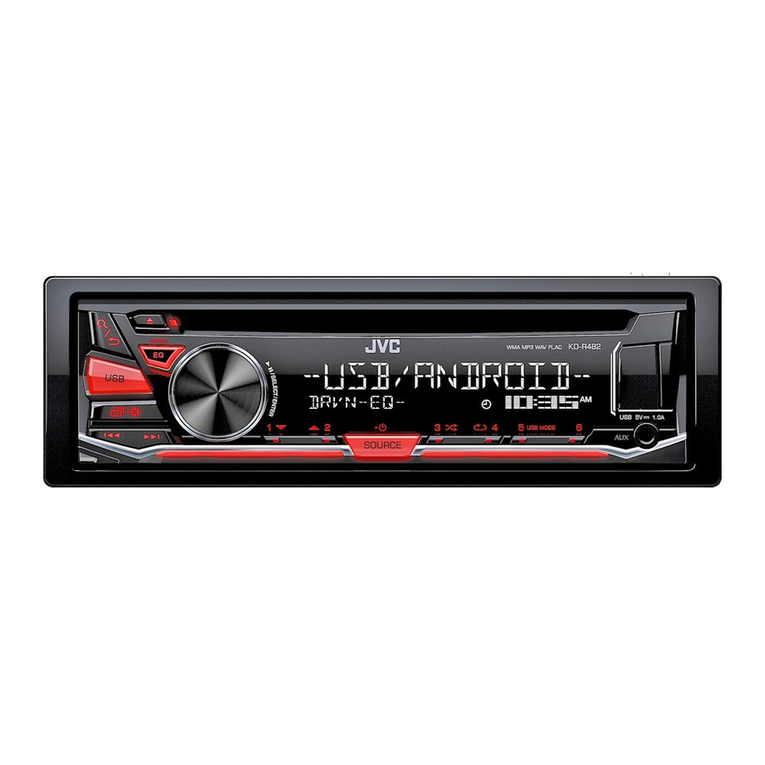
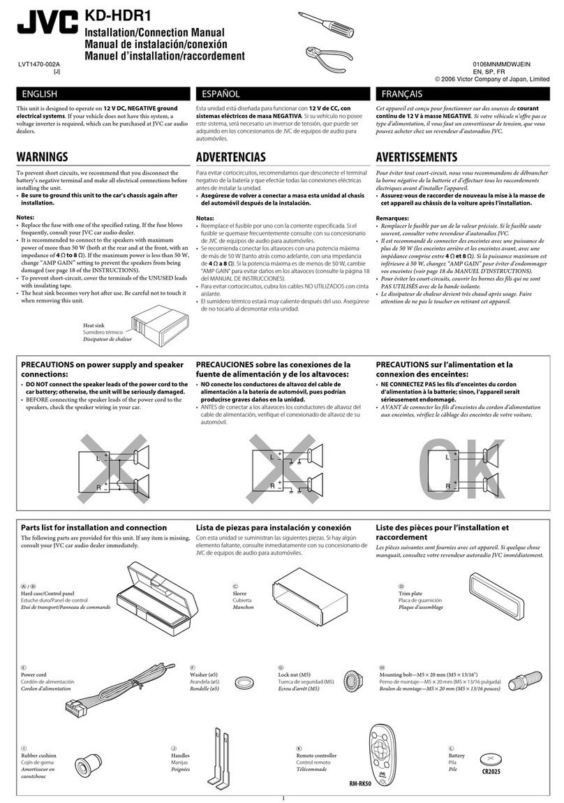
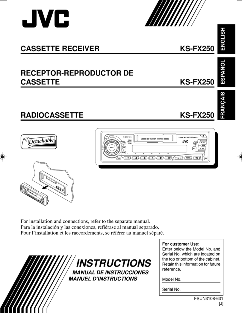
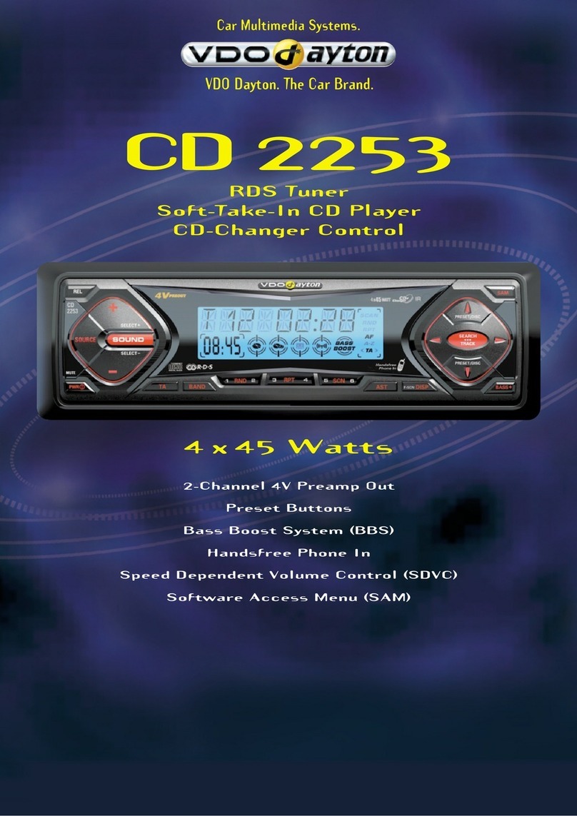
JVC KD-S6250 User manual

SERVICE MANUAL
CD RECEIVER
No.49666
Dec. 2001
COPYRIGHT 2001 VICTOR COMPANY OF JAPAN, LTD.
KD-S6250 / KD-S580
KD-S6250/KD-S580
Area Suffix
J ------ Northern America
KD-S6250
KD-S580
31
FM
CD
AM
SSM
KD-S6250
DIRECT TRACK ACCESS
MO RPT RND
MODE SCM
FM
CD
AM
SSM
KD-S580
DIRECT TRACK ACCESS
MO RPT RND
MODE SCM
Contents
Safety precaution
Preventing static electricity
Disassembly method
Adjustment method
1-2
1-3
1-4
1-11
Flow of functional
operation unit TOC read
Maintenance of laser pickup
Replacement of laser pickup
Description of major ICs
1-12
1-14
1-14
1-15
Difference point
KD-S6250
KD-S580
Color
Silver
Metallic gray
Remocon

KD-S6250/KD-S580
1-4
Press the eject button in the lower right part of the
front panel. Remove the front panel assembly from
the body.
1.
Removing the front panel assembly
(See Fig.1)
Prior to performing the following procedure, remove
the front panel assembly.
Release the four joint tabs aon both sides of the
front chassis assembly and remove the front chassis
assembly toward the front.
1.
Removing the front chassis assembly
(See Fig.2 and 3)
Disassembly method
<Main body>
Fig.1
Fig.2
Fig.3
Front panel assembly
Eject button
Tab a
Tab a
Front chassis assembly
Front chassis
assembly
Heat sink Tab a
Tab a

KD-S6250/KD-S580
1-5
Remove the three screws Aon the left side of the
body.
1.
Removing the heat sink (See Fig.4)
Prior to performing the following procedure, remove
the front panel assembly, the front chassis assembly
and the heat sink.
Turn over the body and unjoint the five joints bwith
the bottom cover and the body using a screwdriver.
1.
Removing the bottom cover
(See Fig.5 and 6)
Fig.4
Fig.5
Fig.6
Heat sink
AA
Joints b
Joints b
Joint b
Joints b
Joints b
Joint b
Bottom cover
Bottom cover
Rear panel
Rear panel

KD-S6250/KD-S580
1-6
Prior to performing the following procedure, remove
the front panel assembly, the front chassis assembly,
the heat sink and the bottom cover.
Remove the screw B, the four screws C and the
three screws Dattaching the rear bracket on the
back of the body. Remove the rear panel.
Remove the two screws Eattaching the main board
on the bottom of the body. Disconnect connector
CN501 on the main board in the direction of the
arrow.
1.
2.
Removing the main board
(See Fig.7 and 8)
Prior to performing the following procedure, remove
the front panel assembly, the front chassis assembly,
the heat sink, the bottom cover and the main board.
Remove the three screws Fattaching the cassette
mechanism section on the back of the top chassis.
1.
Removing the CD mechanism section
(See Fig.9)
Fig.7
Fig.8
Fig.9
Rear panel
B
D
D
D
C
Main board
E
E
CN501
CD mechanism section
F
F
F
Top chassis
CC

KD-S6250/KD-S580
1-7
Prior to performing the following procedure, remove
the front panel assembly.
Remove the four screws Gattaching the rear cover
on the back of the front panel assembly.
Unjoint the eleven(KD-S625)or nine(KD-S580) joints
cwith the front panel and the rear cover.
Remove the control switch board on the back of the
front panel.
1.
2.
3.
Removing the control switch board
(See Fig.10 to 12)
Fig.10
Fig.11
Fig.12
G
GG
G
Rear cover
Joints c
Joints c
Front panel
Rear cover
Front panel
Control switch board
Joints c
Joints c
Joints c
Joints c
Front panel
Rear cover
Joints c
Joints c
(KD-S6250)
(KD-S580)

KD-S6250/KD-S580
1-8
Unsolder the part f and g on the CD mechanism
control board.
Remove the stator fixing the CD mechanism control
board and the damper bracket (To remove the stator
smoothly, pick up the center part).
Remove the screw F attaching the CD mechanism
control board.
Remove the CD mechanism control board in the
direction of the arrow while releasing it from the two
damper bracket slots i and the front bracket slot j.
Disconnect the flexible wire from connector on the
pickup unit.
Removing the CD mechanism control
board(See Fig.1 and 2)
Turn the FD gear in the direction of the
arrow to move the entire pickup unit to
the appropriate position where the
flexible wire of the CD mechanism unit
can be disconnected easily (Refer to
Fig.2).
ATTENTION:
Fig.1
Fig.2
Fig.3
Fig.4
Front bracket
CD mechanism
control board
Shift the lock
Flexible wire
Pickup unit
FD gear
CD mechanism control board
Loading motor Front bracket
Front bracket Pull outward
Pull outward
Flame
Damper bracket
mm
h
i
g
f
II
I
CD mechanism ass’y
Fj
k
G
k
G

KD-S6250/KD-S580
1-9
Prior to performing the following procedure, remove
the CD mechanism control board.
Remove the two springs k attaching the CD mechanism
ass’y and the front bracket.
Remove the two screws G and the front bracket
while pulling the flame outward.
Remove the belt and the screw H from the loading
motor.
Removing the loading motor
(See Fig.3 to 5)
Prior to performing the following procedure, remove
the CD mechanism control PWB and the front
bracket (loading motor).
Remove the three screws I and the damper bracket.
Raise the both sides fix arms and move the fix plates
in the direction of the arrow to place the four shafts l
as shown in Fig.8 and 9.
Remove the CD mechanism ass’y and the two
springs m attaching the flame.
Remove the two screws J and both sides rear
damper brackets from the dampers. Detach the CD
mechanism ass’y from the left side to the right side.
1.
2.
3.
4.
Removing the CD mechanism ass’y
(See Fig.1, 6 to 9)
The CD mechanism ass’y can be
removed if only the rear damper
bracket on the left side is removed.
ATTENTION:
Fig.5
Fig.6
Fig.7
Fig.8
Fig.9
Rear damper bracket
Fix arm (R)
Damper
H
II
Loading motor
Belt
Damper bracket
CD mechanism ass’y
Flame m
m
I
I
Fix plate (L)
l
l
Rear damper bracket
Fix arm (L)
Damper
J
Fix plate(R)
J
l
l

KD-S6250/KD-S580
1-10
Prior to performing the following procedure, remove
the CD mechanism control board, the front bracket
(loading motor) and the CD mechanism ass’y.
Remove the two screws K and the feed motor ass’y.
1.
Removing the feed motor ass’y
(See Fig.10)
*Prior to performing the following procedure, remove
the CD mechanism control board, the front bracket
(loading motor), the CD mechanism ass’y and the
feed motor ass’y.
Detach the FD gear part of the pickup unit upward.
Then remove the pickup unit while pulling out the
part n of the FD screw.
1.
Remove the screw L attaching the nut push spring
plate and the pickup mount nut from the pickup unit.
Pull out the FD screw.
2.
Removing the pickup unit
(See Fig.10 and 11)
When reattaching the pickuap unit,
reattach the part o of the pickup unit,
then the part n of the FD screw.
ATTENTION:
Prior to performing the following procedure, remove
the CD mechanism control board, the front bracket
(loading motor), the CD mechanism ass’y and the
feed motor ass’y.
Turn up the CD mechanism ass’y and remove the
two springs p on both sides of the clamper arms.
Open the clamper arm upward.
Turn the turn table, and remove the two screws M
and the spindle motor.
1.
2.
Removing the spindle motor
(See Fig.12 and 13)
Fig.10
Fig.11
Fig.12
Fig.13
Spindle motor
pp
Pickup unit
Part n
FD screw
Feed motor ass’y
FD gear Pickup unit
Part O
K
Nut push spring plate
Pickup mount nut
Pickup unit
FD screw
L
M
M
KD-S6250/KD-S580
1-11
Adjustment method
Test instruments required for adjustment
1. Digital oscilloscope (100MHz)
2. AM Standard signal generator
3. FM Standard signal generator
4. Stereo modulator
5. Electric voltmeter
6. Digital tester
7. Tracking offset meter
8. Test Disc JVC :CTS-1000
9. Extension cable for check
EXTGS004-26P 1
Standard measuring conditions
Power supply voltage DC14.4V(10.5~16V)
Load impedance 20Kohm(2 Speakers connection)
Output Level Line out 2.0V (Vol. MAX)
How to connect the extension cable for adjusting
Dummy load
Exclusive dummy load should be used for AM,and FM. For
FM dummy load,there is a loss of 6dB between SSG output
and antenna input.The loss of 6dB need not be considered
since direct reading of figures are applied in this working
standard.
Standard volume position
Balance and Bass &Treble volume : lndication"0"
Loudness : OFF
BBE : OFF
Frequency Band
FM 87.5MHz ~ 107.9MHz
AM 530kHz ~ 1710 kHz
EXTGS004-26P
The cardboard is cut in a suitable size.
uses for the insulation stand of mechanism.

KD-S6250/KD-S580
1-12
Power ON
Set Function to CD
Play
Jump to the first track
TOC readout
Tracking loop closed
Disc rotates
Disc inserted
YES
YES
Laser emitted
Pickup feed to the inner area
Focus search
RF signal eye-pattern
opens
RF signal eye-pattern
remains closed
"No disc"
display
•When correctly focused
Focus Servo Loop ON
•When the laser diode correctly
emits
Microprocessor
commands
Rough Servo Mode
CLV Servo Mode
(ProgramArea)
CLV Servo Mode
(Lead-In Area;
Digital: 0)
•RF signal
Flow of functional operation until TOC read
•When the pickup correctly moves
to the inner area of the disc
TERMINAL
Microprocessor
commands
FMO
TC9462 "53"
FEED MOTOR
+TERMINAL
IC581 "5"
REST SW
•When the disc correctly rotates
Tracking Servo Loop ON
Servo CLV
Rough
Servo
AccelerationAcceleration
Microprocessor
commands
Spindle
motor (-)
IC581 "7"
0.5 Sec 0.5 Sec

KD-S6250/KD-S580
1-13
Feed Section
Focus Section
Tracking Section
Spindle Section
Is the voltage output at
IC521 pin "53" 5V or 0V?
Check the feed motor.
Is 4V present at both
sides of the feed motor?
Is the wiring for IC521
(90) ~ (100) correct?
Check IC581.
Is 6V or 2V present at
IC581 "5" and "6"?
Is 5V present at IC581
pin "11"?
Check the feed motor
connection wiring.
Check the vicinity of
IC521.
Check CD 9V
and 5V.
YES
YES
YES
NONO
NO
NO
NO
YES
YES
When the lens is
moving: Check the circuits in
the vicinity of IC581
pins "15" ~ "18".
Check the pickup and
its connections.
NO
YES
YES
YES
Does the S-search
waveform appear at
IC581 pins "17" and "18"?
Is the disk rotated?
Does the RF signal
appear at TP1?
Is 4V present at IC581
pins "7" and "8" ?
Check the spindle motor
and its wiring.
Is 4V present at IC521
pin "55" ?
Check the vicinity of
IC581.
Check IC501 and
IC521.
YES
NO
NO
NO
NO NO
YES
YES
YES
Check the circuits in the
vicinity of IC501 "19" ~
"24" or the pickup
Is the RF waveform at TP1
distorted?
Proceed to the Tracking
section
When the disc is rotated
at first:
Check the circuit in the
vicinity of IC501 pins
"2" ~ "12".
Check IC521.
Check the pickup and
its connections.
YESYES
YES
Is the tracking error signal
output at IC501 "12"?
Approx. 1.2 V
4V

KD-S6250/KD-S580
1-14
Maintenance of laser pickup
(1) Cleaning the pick up lens
Before you replace the pick up, please try to
clean the lens with a alcohol soaked cotton
swab.
(2) Life of the laser diode
When the life of the laser diode has expired,
the following symptoms will appear.
(1) The level of RF output (EFM output:ampli
tude of eye pattern) will be low.
Replacement of laser pickup
Is RF output
1.0 0.35Vp-p? Replace it.
NO
YES
O.K
(3) Semi-fixed resistor on the APC PC board
The semi-fixed resistor on the APC printed
circuit board which is attached to the pickup
is used to adjust the laser power.Since this
adjustment should be performed to match the
characteristics of the whole optical block,
do not touch the semi-fixed resistor.
If the laser power is lower than the specified
value,the laser diode is almost worn out, and
the laser pickup should be replaced.
If the semi-fixed resistor is adjusted while
the pickup is functioning normally,the laser
pickup may be damaged due to excessive current.
Turn off the power switch and,disconnect the
power cord from the ac outlet.
Replace the pickup with a normal one.(Refer
to "Pickup Removal" on the previous page)
Plug the power cord in,and turn the power on.
At this time,check that the laser emits for
about 3seconds and the objective lens moves
up and down.
Note: Do not observe the laser beam directly.
Play a disc.
Check the eye-pattern at TP1.
Finish.

KD-S6250/KD-S580
1-15
2
1
11
12
10
15 13
14
5
4
6
3
8
9
7
ILM AJGND
C6
10u
C5
0.1u
C4
0.1u
C3
0.1u
AUDIO OUT
CD OUT
CTRL
ANT CTRL
EXT OUT
ANT OUT
VCC ACC
Surge Protector
BIAS TSD
C1
100u C2
0.1u
+B
ACC
BATT.DET OUT
COMPOUT
VDD OUT
SW5VOUT
ILMOUT
C7
0.1u
C8
0.1u
R1
UNIT R:
C:F
note1) TAB (header of IC)
connected to GND
HA13164 (IC901) : Regulator
1.Terminal layout
2.Block diagram
3.Pin function
Pin No. Symbol Function
1
2
3
4
5
6
7
8
9
10
11
12
13
14
15
EXTOUT
ANTOUT
ACCIN
VDDOUT
SW5VOUT
COMPOUT
ANT CTRL
VCC
BATT DET
AUDIO OUT
CTRL
CD OUT
ILM AJ
ILM OUT
GND
Output voltage is VCC-1 V when M or H level applied to CTRL pin.
Output voltage is VCC-1 V when M or H level to CTRL pin and H level
to ANT-CTRL.
Connected to ACC.
Regular 5.7V.
Output voltage is 5V when M or H level applies to CTRL pin.
Output for ACC detector.
L:ANT output OFF , H:ANT output ON
Connected to VCC.
Low battery detect.
Output voltage is 9V when M or H level applied to CTRL pin.
L:BIAS OFF, M:BIAS ON, H:CD ON
Output voltage is 8V when H level applied to CTRL pin.
Adjustment pin for ILM output voltage.
Output voltage is 10V when M or H level applies to CTRL pin.
Connected to GND.
123456789101112131415
Description of major ICs

KD-S6250/KD-S580
1-16
1.Pin layout
2.Block diagram
AN8806SB-W (IC501) : RF & Servo amp.
PD 1
LD 2
LDON 3
LDP 4
VCC 5
RF- 6
RF OUT 7
RF IN 8
C.AGC 9
ARF 10
C.ENV 11
C.EA 12
CS BDO 13
BDO 14
CS BRT 15
OFTR 16
/NRFDET 17
GND 18
36 PDAC
35 PDBD
34 PDF
33 PDE
32 PDER
31 PDFR
30 TBAL
29 FBAL
28 EF-
27 EF OUT
26 TE-
25 TE OUT
24 CROSS
23 TE BPF
22 VDET
21 LD OFF
20 VREF
19 ENV
30 24 25 26 23 22 14 3
33
32
34
31
36
35
13
14
15
16
20
2
21
629
728
27 8910 17 11 12 19
ENV CURCUIT
RF
DET
AGC
EQ
BDO
OFTR
-
+
VCBA
VCBA
VCBA
+
-
+
-
-
+
-
+
-
+
-
+
-
+
-
+
-
+
-
+
-
+
- +
-
+
+ -
+
-
- + - +
VCBA

KD-S6250/KD-S580
1-17
35
36
34
33
32
31
30
29
28
27
26
25
24
23
22
21
20
19
18
17
16
15
14
13
12
11
10
9
8
7
6
5
4
3
2
1
3. Pin function
PD AC
FBAL
TBAL
PDFR
PDER
PDF
PDE
PD BD
TE BPF
VDET
CROSS
TE OUT
TE-
FE OUT
FE-
/NRFDET
GND
LD OFF
VREF
ENV
OFTR
C.AGC
ARF
C.ENV
C.EA
CS BDO
BDO
CS BRT
LD
LD ON
LDP
VCC
RF-
RF OUT
RF IN
PD
Pin No. Symbol I/O
I
O
I
--
--
I
O
I
I/O
O
I/O
I/O
I/O
O
I/O
O
O
--
O
O
--
O
I
O
O
I
O
I
I
I
I/O
I/O
I
I
I
I
Function
APC amp . Input terminal
APC amp . Output terminal
LD ON/OFF control terminal
Connect to GND
Power supply
RF amp . Reversing input terminal
RFamp . Output terminal
AGC input terminal
AGC loop filter connection terminal
ARF output terminal
RF detection capacity connection terminal
HPF-amp capacity connection terminal
Capacity connection terminal for RF discernment side envelope detection
BDO output terminal
Capacity connection terminal for RF discernment side envelope detection
OFTR output terminal
RFDET output terminal
Connect to GND
3TENV output terminal
VREF output terminal
APC OFF control terminal
VDET output terminal
VDET input terminal
CROSS output terminal
TE amp . Output terminal
FE amp . Reversing input terminal
FE amp . output terminal
FE amp . Reversing input terminal
F.BAL control terminal
T.BAL control terminal
I-V amp conversion resistance adjustment terminal
I-V amp input terminal
AN8806SB-W

KD-S6250/KD-S580
1-18
11
6 20
1
4
10
15
25
13
14
16
12
9
8
5
7
2
22
17
19
18
21
23
24
3
-
+
-
+
-
+
-
+
-
+
-
+
-
+
-
+
IN 1
IN 2
ST BY
Vcc 1/2 Vcc 3/4
OUT 1+
OUT 1-
PWR GND1
OUT 2+
OUT 2-
PWR GND2
R.F
IN 3
IN 4
PRE GND
ON TIME C Muting &
ON Time Control
Circuit
Protective
circuit
Protective
circuit
Mute
circuit
Ripple
Filter
Stand by
Switch
N.C
+
+
0.22 F
2200 F 0.022 F
0.22 F
TAB
+5V
ST ON
+
+
+
+
47 F
0.22 F
0.22 F
22 F
+
Mute 10K
+
3.3 F
OUT 3+
OUT 3-
Low Level
Mute ON
PWR GND3
OUT 4+
OUT 4-
PWR GND4
LA4743K(IC321):Power AMP
1.Block diagram

KD-S6250/KD-S580
1-19
2.Terminal layout
3.Pin function LA4743K
TAB
GND
OUTRR-
STBY
OUTRR+
VCC1/2
OUTRF-
GND
OUTRF+
RIPPLE
INRF
INRR
SGND
INLR
INLF
ONTIME
OUTLF+
GND
OUTLF-
VCC3/4
OUTLR+
MUTE
OUTLR-
GND
NC
1
2
3
4
5
6
7
8
9
10
11
12
13
14
15
16
17
18
19
20
21
22
23
24
25
SymbolPin No. Function
Header of IC
Power GND
Outpur(-) for front Rch
Stand by input
Output (+) for front Rch
Power input
Output (-) for rear Rch
Power GND
Output (+) for rear Rch
Ripple filter
Rear Rch input
Front Rch input
Signal GND
Front Lch input
Rear Lch input
Power on time control
Output (+) for rear Lch
Power GND
Output (-) for rear Lch
Power input
Output (+) for front
Muting control input
Output (-) for front
Power GND
Non connection

KD-S6250/KD-S580
1-20
VCC2
V05-
V05+
V04+
V04-
V03+
V03-
V02+
V02-
V01+
V01-
VCC1
VIN1
VIN1G
FR
REV
FWD
S-GND
VCONT
VIN4
VIN4G
VCC-S
VREF-IN
REG-OUT
REG-IN
VIN3G
VIN3
VIN2G
VIN2
FR
28
27
26
25
24
23
22
21
20
19
18
17
16
15
FR
1
2
3
4
5
6
7
8
9
10
11
12
13
14
FR
CH 3,4,5
Power supply
Output control
CH5
CH4
CH2
CH1
CH3
22K 11K
5VREG(PNPTr
The outside putting)
22K
22K
22K
11K
11K
11K
CH1,2
Power supply
LA6567H-X(IC581):CD DRIVER
1.Pin layout & blockdiagram
Level shiftLevel shiftLevel shiftLevel shift
Thermal shutdown
Input
Signal system power supply

KD-S6250/KD-S580
1-21
2. Pin function
1
2
3
4
5
6
7
8
9
10
11
12
13
14
15
16
17
18
19
20
21
22
23
24
25
26
27
28
Pin no. Symbol
CH3,4,5 Power supply( It is short with VCC1,VCC-S)
Loading output(-)
Loading terminal (+)
CH4 Output terminal(+)
CH4 Output terminal(-)
CH3 Output terminal(+)
CH3 Output terminal(-)
CH2 Output terminal(+)
CH2 Output terminal(-)
CH1 Output terminal(+)
CH1 Output terminal(-)
CH1,2(BTL) Power supply(It is short with VCC-S,VCC2)
CH1 Input terminal
CH1 Input terminal(For gain adjustment)
CH2 Input terminal
CH2 Input terminal(For gain adjustment)
CH3 Input terminal
CH3 Input terminal(For gain adjustment)
Regulator terminal(Outside putting PNP base)
Regulator terminal(Outside putting PNP collector)
Standard voltage input terminal
Signal system power supply(It is short with VCC1,VCC2)
CH4 Input terminal(For gain adjustment)
CH4 Input terminal
5CH(VLO) Output voltage set terminal
Signal system GND
5CH(VLO)Signal output switch terminal(FWD),Input of logic of loading part
5CH(VLO)Signal output switch terminal(REV),
Input of logic of loading part
Function
VCC2
V05-
V05+
V04+
V04-
V03+
V03-
V02+
V02-
V01+
V01-
VCC1
VIN1
VIN1G
VIN2
VIN2G
VIN3
VIN3G
REG-IN
REG-OUT
VREF-IN
VCC-S
VIN4G
VIN4
VCONT
S-GND
FWD
REV
LA6567H-X(2/2)
Frame(FR)at the center becomes system GND.
Please be short-circuited on the outside and use the terminal of the power supply system
and three teminals of VCC-S, VCC1,VCC2.

KD-S6250/KD-S580
1-22
I/O
LC72366-9A73 (IC801) : System CPU
Symbol FunctionPin No.
XIN
TEST2
J-BUS SI
J-BUS SO
J-BUS SCK
J-BUS I/O
SUBQ
SQCK
RESET
LCD SI
LCD SO
LCD SCK
LCD CE
FM ILLUMI
AM ILLUMI
CD ILLUMI
DIMMER OUT
LM0
LM1
KS2
KS1
KS0
DETACH
K2
K1
K0
Vdd
SW2
CD LSI RESET
MCLK
MDATA
MLD
SCL
SDA
I
I
-
-
-
-
I/O
-
I/O
I
-
O
O
O
-
-
-
-
O
O
-
-
-
O
O
O
I
-
I
I
-
I
O
O
O
O
-
-
O
O
Crystal oscillator input port
Connect to ground
CD LSI subcode data input
No use
CD LSI subcode clock
Micon reset pin
No use
LCD driver data output
LCD driver clock signal
LCD driver chip enable port
No use
No use
No use
No use
CD loading motor output
No use
No use
No use
Output for initial setting diode matrix
Front panel detect
No use
Input for initial setting diode matrix
5V power supply port (+B)
CD mechanism detect switch
CD LSI reset
CD LSI command clock signal
CD LSI command data output
CD LSI command load signal
No use
No use
E.volume clock output
E.volume data output
1
2
3
4
5
6
7
8
9
10
11
12
13
14
15
16
17
18
19
20
21
22
23
24
25
26
27
28
29
30
31
32
33
34
35
36
37
38
39
40
1. Pin layout
2. Pin function
24 ~ 1
41 ~ 64
25
40
~
80
65
~
No use
No use
No use
No use
Other manuals for KD-S6250
1
This manual suits for next models
1
Table of contents
Other JVC Car Receiver manuals