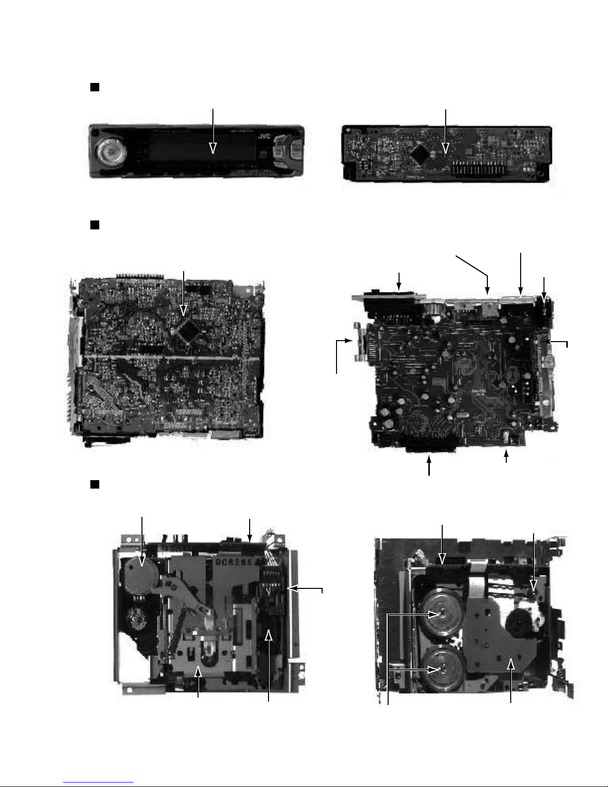
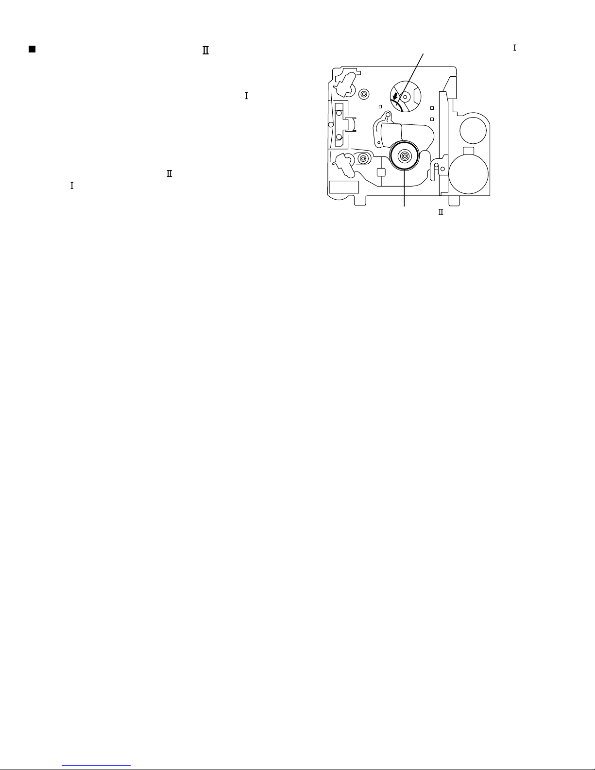
JVC KS-FX915R User manual

SERVICE MANUAL
CASSETTE RECEIVER
No.49613
Feb. 2001
COPYRIGHT 2001 VICTOR COMPANY OF JAPAN, LTD.
KS-FX915R/KS-FX815
KS-FX915R/KS-FX815
MO
TPTP
RDSRDS
PTYPTY
DISPDISP
8 9 10 11 127
DAB
MO
DISPDISP
SCANSCAN
LOUDLOUD
8 9 10 11 127
KS-FX915R
KS-FX815
KS-FX815
KS-FX915R
Area Suffix
EE Russian Federation
Contents
Safety precaution 1- 2
Location of main parts 1- 3
Disassembly method 1- 4
Adjustment method
Description of major ICs 1-14
1-11
Difference point
KS-FX915R
KS-FX815
Dimmer Beep
RDS LCD Remocon
O
X
Color
Nega
O
X
O
X
O
X

KS-FX915R/KS-FX815
1-2
!Burrs formed during molding may be left over on some parts of the chassis. Therefore,
pay attention to such burrs in the case of preforming repair of this system.
Safety precaution

KS-FX915R/KS-FX815
1-3
Location of main parts
Control unit
Display Control unit
Main unit
Main board
Main board assembly
Power IC
Connector to controller
Tuner
pack
Antenna
jack
RCA jack
Changer control
connector
I/O connector
Cassette mechanism
Main board assembly
Connector to controller
Cassette mechanism
C.motor assembly Mechanism control board assembly
Cassette housing Head
Head relay board
Mechanism control board assembly
Flywheel assembly Reel board
Capstan motor assembly

KS-FX915R/KS-FX815
1-4
Disassembly method
Removing the front chassis
(See Fig.1)
1. Remove two screws Aand insert a screwdriver to the
joints aon the side of the front chassis and two joints b
on the right side, then detach the front chassis toward the
front side.
Removing the heat sink (See
Fig.2 )
1. Remove the three screws Battaching the heat sink on
the left side of the body, and remove the heat sink.
Removing the bottom cover (See
Fig.3 )
1.
2.
Turn the body upside down.
Insert a screwdriver to the two joints c and two joints d on
both sides of the body and the joint e on the back of the
body, then detach the bottom cover from the body.
Fig.1
Fig.2
Front chassis
b
a
a
b
Heat sink
B
B
B
Fig. 3
Regulator board
ed
c
A
A

KS-FX915R/KS-FX815
1-5
Removing the main amplifier board assembly
(See Fig.4 and 5)
1.
2.
3.
4.
5.
Remove the front chassis.
Remove the bottom cover.
Remove the two screws C attaching the main amplifier
board assembly on the bottom of the body.
Remove the three screws Dattaching the main amplifier
board assembly on the back of the body.
Disconnect connector CP401 on the main amplifier board
assembly from the cassette mechanism assembly.
Removing the Cassette mechanism assembly
(See
Fig.6 )
1.
2.
3.
4.
Remove the front chassis.
Remove the bottom cover.
Remove the main amplifier board assembly.
Remove the four screws Eattaching the Cassette
mechanism assembly from the top cover.
Removing the control switch board
(See
Fig.7 and 8 )
1.
2.
3.
Remove the front chassis.
Remove the four screws Fattaching the rear cover on the
back of the front panel unit.
Remove the control switch board from the front panel
unit.
Fig. 5
D
D
F
F
F
F
Fig. 7
Fig. 8
Control switch board
E
Fig. 6
E
Fig.4
C
C
Main amplifier board
CP401

KS-FX915R/KS-FX815
1-6
For the 6pin wire extending from connector CN402
on the head amplifier board, disconnect it from the
head relay board.
Disconnect the card wire from connector CN403 on
the head amplifier board.
Remove the screw Aattaching the head amplifier
board.
Move the tab aas shown in Fig.2 and remove the
head amplifier board while moving it in the direction
of the arrow.
1.
2.
3.
4.
<Removal of the cassette mechanism>
Removing the head amplifier board.
(See Fig.1 and 2)
Disconnect the 6pin wire from connector CN402 and
the card wire from CN403 on the head amplifier
board (Refer to Fig.1 and 2).
Remove the four screws Bon the bottom of the
cassette mechanism.
1.
2.
Removing the cassette mechanism
assembly (See Fig.1 to 3)
Fig.1
Cassette mechanism ass’y
Head relay
board
6pin
wire
CN402 CN403
CN402
Head amplifier board
Fig.2
Tab a
Head amplifier board
Fig.3
Cassette mechanism ass’y
B
B
A
Head amplifier board
CN403

KS-FX915R/KS-FX815
1-7
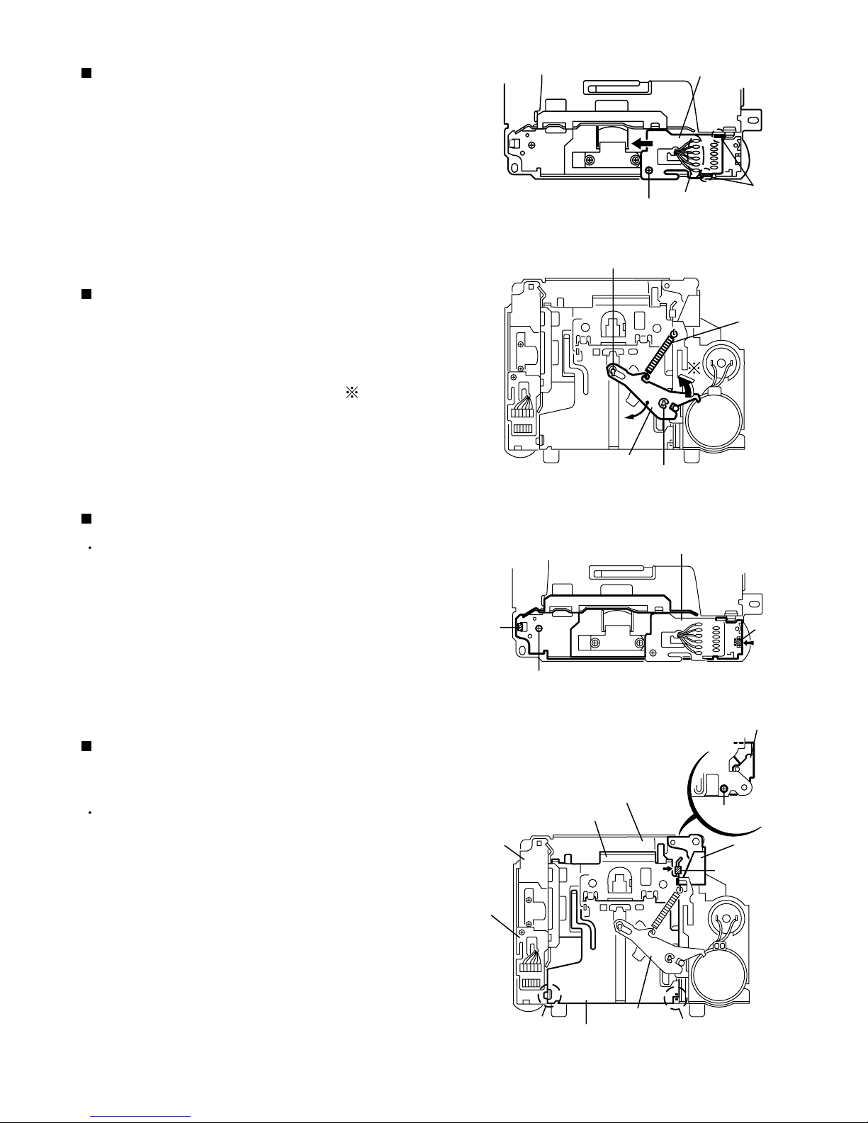
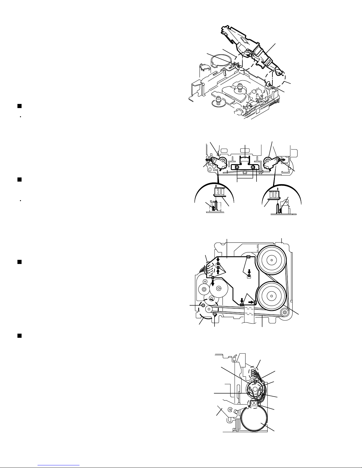
Unsolder the soldering bon the head relay board.
Remove the screw Cattaching the head relay board.
Remove the head relay board in the direction of the
arrow while releasing the two joints c.
1.
2.
3.
Removing the head relay board
(See Fig.4)
Remove the E washer attaching the load arm using
a pincette or something like that and remove the
spring d.
Move the part of the load arm marked upwards to
release it from the axis of rotation. Then rotate the
load arm in the direction of the arrow to remove it
from the cach.
1.
2.
Removing the load arm (See Fig.5)
Prior to performing the following procedure, remove
the head relay board.
Remove the screw Dattaching the sub chassis.
Push the tab ein the direction of the arrow to detach
the one side of the sub chassis. Then release the
sub chassis from the tab f.
1.
2.
Removing the sub chassis (See Fig.6)
Prior to performing the following procedure, remove
the head relay board, the load arm and the sub
chassis.
Remove the screw Eattaching the reinforce bracket.
Remove the reinforce bracket.
Push the tab gfixing the cassette holder in the
direction of the arrow and open the cassette holder
and the holder arm upward until they stop at an
angle of 45 degrees. Move the two joints hto the
side and remove the cassette holder and the holder
arm from the shaft.
1.
2.
3.
Removing the cassette holder and the
holder arm in the eject mode
(See Fig.7 and 8)
Fig.4 CSoldering b Joint c
Fig.6
Tab f
D
Tab e
Cach
Head relay board
Head relay board
Fig.7
Reinforce bracket
Reinforce
bracket
E
Cassette holder
Sub chassis
Head relay
board
Joint h
Holder arm
Load arm
Joint h
tab g
Fig.5
Spring d
Load arm E washer
Cassette mecha chassis

KS-FX915R/KS-FX815
1-8
Prior to performing the following procedure, remove
the head relay board and the sub chassis.
Remove the two screws Fattaching the play head
(The spring under the play head comes off at the
same time).
1.
Removing the play head (See Fig.9)
Prior to performing the following procedure, remove
the head relay board and the sub chassis.
Push each tab i in the direction of the arrow and pull
out the pinch rollers on both sides.
1.
Removing the pinch roller ass’y
(See Fig.9)
Unsolder the soldering jon the reel disc board.
Push the seven tabs kon the bottom of the cassette
mechanism assembly in the direction of the arrow.
1.
2.
Removing the reel disc board
(See Fig.10)
Unsolder the two soldering lof the motor and the sub
motor.
Release the sub motor from the three tabs m. Push
the sub motor upward and pull out it.
Remove the belt on the bottom of the cassette
mechanism assembly and remove the two screws G
attaching the motor.
1.
2.
3.
Removing the motor and the sub motor
(See Fig.10 and 11)
The motors can be detached before
removing the load arm.
ATTENTION:
Fig.8
Cassette holder
and holder arm
Joint h
Shaft
Shaft
Joint h
Fig.9
Tab i
Pinch roller ass’yPinch roller ass’y
F
Play head
Spring
Fig.11
Sub motor
Tab m
Load arm
Motor
Soldering l
Tab m
Soldering l
Tab m
Soldering j
Pinch roller ass’y
Tab i Tab i
Tab i
Fig.10
Cassette mechanism ass’y
Tabs k
Reel disc board
Soldering j
Tabs k
G
G
Motor Belt
Flyhwheel

KS-FX915R/KS-FX815
1-9
Prior to performing the following procedure, remove
the head relay board, the load arm, the sub chassis,
the cassette holder, the holder arm and the reel disc
board.
Remove the belt on the bottom of the cassette
mechanism ass’y.
Remove the slit washer attaching the flywheel on the
upper side of the cassette mechanism ass’y and pull
out the flywheel downward. Then remove another
flywheel in the same way.
1.
2.
3.
Removing the flywheel
(See Fig.10 and 12)
Prior to performing the following procedure, remove
the head relay board, the load arm, the sub chassis,
the cassette holder and the holder arm.
Disengage the part ninside of the reel driver which
engages with the shaft, using a pincette or
something like that. Then remove the reel driver from
the shaft.
Remove the reel driver spring and the reel table.
1.
2.
Removing the reel disc ass’y( )
(See Fig.12 to 14)
When reassembling, make sure to use
a new slit washer.
ATTENTION:
Fig.10
Cassette mechanism ass’y
Tab k
Reel disc board
Soldering j
Tab k
G
G
Motor Belt
Flyhwheel
Fig.12
Plate
The part n
Reel driver
Reel disc ass’y( )
Push aside
the gear
Tabs o
Reel disc
ass’y( )
The part n
Reel driver
Tab o
Fig.13
Reel driver
Shaft
The part n
Fig.14
Reel driver spring
Reel table
Slit washer
Slit washer

KS-FX915R/KS-FX815
1-10
Release the plate from the three tabs o.
Push aside the gear over the reel table using a
pincette or something like that.
Remove the reel disc ass’y ( ) as with the reel disc
ass’y ( ).
1.
2.
3.
Removing the reel disc ass’y( )
(See Fig.12 to 15)
Do not break the front panel tab fitted
to the metal cover.
ATTENTION:
Prior to performing the following
procedure, remove the reel disc ( ).
ATTENTION:
Fig.15
Push aside the gear and reattach the reel disc Ass’y( ).
Reel disc ass’y( )

KS-FX915R/KS-FX815
1-11
Adjustment method
1.Digital osclloscope(100MHz)
Measuring conditions(Amplifier section)
Power supply voltage
Load impedance
Line out
Standard volume position
Balance and Bass,Treble volume .Fader
:Center(Indication"0")
Loudness,Dolby NR,Sound,Cruise:Off
Volume position is about 2V at speaker output with
following conditions.Playback the test tape VT721.
AM mode 999kHz/62dB,INT/400Hz,30%
modulation signal on receiving.
FM mono mode 97.9MHz/66dB,INT/400Hz,22.5kHz
deviation pilot off mono.
FM stereo mode 1kHz,67.5kHz dev. pilot7.5kHz dev.
Output level 0dB(1 V,50 /open terminal).
for DOLBY level measurement
For playback frequency measurement
For wow flutter & tape speed measurement
For head azimuth measurement
Cassette type for CTG-N
(mechanism adjustment)
DC14.4V(10.5~16V)
4 (2Speakers connection)
20k
Tuner section
BAND STEP
FM : 100kHz (Seek), 50kHz (Manual)
AM : 9kHz step
DUMMY LOAD
Exclusive dummy load should be used for AM
and FM dummy load,there is a loss of 6dB
between SSG output and antenna input. The
loss of 6dB need not be considered since
direct reading of figures are applied in this
working standard.
Arrangement of Adjusting
Cassette Mechanism Section
Preset Memory Initialization
Preset Memory
Band M1 M2
97.9
216
M3
603
M4
105.9
999
M5
108.0
1404
M6
87.5
1620
FM(MHz)
AM(kHz)
Azimuth screw
(Forward side)
Azimuth screw
(Reverse side)
Playback head
Tape speed adjust
Capstan motor
Cassette mechanism
(Surface)
Test Instruments reqired for adjustment
2.Frequency Counter meter
3.Electric voltmeter
4.Wow & flutter meter
5.Test Tapes
VT724
VT739
VT712
VT703
6.Torque gauge
87.5
153
89.9

KS-FX915R/KS-FX815
1-12
1
C401
C402
C403
C404
C405
C406
C407
C408
C409
C410
C411
C412
C413
C414
C415
C416
C417
C418
C419
CP401
CP402
CP403
D401
D402
D403
IC401
IC402
Q401
Q402
Q403
R401
R402
R403
R404
R405
R406
R407
R408
R409
R410
R411
R412
R413
R414
R415
R416
R417
R418
R419
R420
R421
R422
R423
R424
R425
VR402 VR401
B403
B415
B413
B407
B416
B406
B414
B405
B412
B404
B410
B402
B408
B401 B409
B411
1
11
21
1
17
1
2
E
1
1
FSMW1101A
31
TPP
VR402:Rch
(Dolby NR level adj)
VR401:Rch
(Dolby NR Frequency response adj)
Arrangment of adjusting
Head amplifier board section (Reverse side)
Information for using a car audio service jig
1. We're advancing efforts to make our extension cords common for all car audio products.
Please use this type of extension cord as follows.
2. As a U-shape type top cover is employed, this type of extension cord is needed to check operation of the
mechanism assembly after disassembly.
3. Extension cord : EXTKSRT002-18P ( 18 pin extension cord ) For connection between mechanism assembly
and main board assembly.
Check for mechanism driving section such as motor ,etc..
Disassembly method
1. Remove the bottom cover.
2. Remove the front panel assembly.
3. Remove the top cover .
4. Install the front panel.
5. Confirm that current is being carried by connecting
an extension cord jig.
Note
Available to connect to the CP701 connector when in-
stalling the front panel.
Cassette mechanism
Front panel assembly
EXTKSRT002-18P
Extension cord
Main board
Main board
EXTKSRT002-18P
to Main board
to Cassette mechanism

KS-FX915R/KS-FX815
1-13
Item Conditions Adjustment and Confirmation methods S.Values Adjust
Head
azimuth
adjustment
Head height adjustment
Adjust the azimuth directly. When you
adjust the height using a mirror tape,
remove the cassette housing from the
mechanism chassis. After installing the
cassette housing, perform the azimuth
adjustment.
Load the SCC-1659 mirror tape. Adjust with
height adjustment screw A and azimuth
adjustment screw B so that line A of the
mirror tape runs in the center between Lch
and Rch in the reverse play mode.
After switching from REV to FWD then to
REV, check that the head position set in
procedure 1 is not changed. (If the position
has shifted, adjust again and check.)
Adjust with azimuth adjustment screw B so
that line B of the mirror tape runs in the
center between Lch and Rch in the forward
play mode.
Test tape:
SCC-1659
VT703(10kHz)
Test tape: VTT712
(3kHz)
Test tape: VTT724
(1kHz)
VTT739
(63Hz / 1kHz / 10kHz)
1.
Tape speed
and wow
flutter
confirmation
2.
Play back
frequency
response
confiramation
3.
1.
2.
3.
Check to see if the reading of the F, counter /
wow flutter meter is within 3015 3045(FWD
/ REV), and less than 0.35% (JIS RMS).
In case of out of specification, adjust the
motor with a built-in volume resistor.
1.
2.
Play test tape VTT724, and set the volume
position at 2V.
Play test tape VTT739 and confirm.
1kHz / 10kHz: -1 3dB,
1kHz / 63Hz: 0 3dB,
When 10kHz is out of specification, it will be
necessary to read adjust the azimuth.
1.
2.
3.
Load VTT724 (VT724) (1kHz) and play it
back in the reverse play mode. Set the Rch
output level to max.
Load VTT703 (VT703) (10kHz) and play it
back in the forward play mode. Adjust the
Rch and Lch output levels to max, with
azimuth adjustment screw B. In this case,
the phase difference should be within 45 .
Engage the reverse mode and adjust the
output level to max, with azimuth
adjustment screw C.
(The phase difference should be 45 or
more.)
When switching between forward and
reverse modes, the difference between
channels should be within 3dB. (Between
FWD L and R, REV L and R.)
When VTT721 (VT721) (315Hz) is played
back, the level difference between channels
should be within 1.5dB.
1.
2.
3.
4.
5.
Head azimuth adjustment
Tape speed:
3015
3045Hz
Wow
flutter: less
than 0.35%
Speaker out
1kHz / 63Hz
: 0 3db
1kHz / 10kHz
: -1 3db
Built-in volume
resistor
The tuner section is of an adjustment-freedesign. In case the tuner is in trouble, replace the tuner pack.
A line
B line
Head shield
PBHead
FWD Adj B
REV Adj C HEIGHT Adj A
phase
(0 ) (45 )
Head shield
The head is at low position
during.
The head is at High position
during REV.
Output
level:
Maximum

KS-FX915R/KS-FX815
1-14
1
2
3
4
5
6
7
8
9
10
11
12
13
14
15
16
32
31
30
29
28
27
26
25
24
23
22
21
20
19
18
17
SDA
GND
OUTLR
OUTLF
TL
B2L
B1L
IVL
ILL
QSL
IDL
MUTE
ICL
IMD
IBL
IAL
SCL
VCC
OUTRR
OUTRF
TR
B2R
B1R
IVR
ILR
QSR
IDR
Vref
ICR
CAP
IBR
IAR
CD-CH
TAPE
TUNER
POWER
SUPPLY
SOURCE
SELECTOR
VOLUME 1
+20 to -31 dB
LOUDNESS
LEFT
BASS
LEFT
+15 dB
TREBLE
LEFT
+12 dB
BASS
RIGHT
+15 dB
TREBLE
RIGHT
+12 dB
MUTE
FUNCTION
ZERO CROSS
DETECTOR
VOLUME 2
0 to 55 dB
BALANCE
FENDER REAR
VOLUME 2
0 to 55 dB
BALANCE
FENDER FRONT
HC BUS
REC
VOLUME 2
0 to -55dB
BALANCE
FENDER FRONT
VOLUME 2
0 to -55dB
BALANCE
FENDER REAR
VOLUME 1
+20 to -31 dB
LOUDNESS
RIGHT
LOGIC
21
31
2
19
16
15
13
11
22
20
18
17
14
23 25 24 26 27 28
30
29
1
32
3
4
10 8 9 7 6 512
1.Pin layout
3.Pin functions
2.Block diagram
1
2
3
4
5
6
7
8
9
10
11
12
13
14
15
16
Pin
No. Pin
No.
17
18
19
20
21
22
23
24
25
26
27
28
29
30
31
32
SDA
GND
OUTLR
OUTLF
TL
B2L
B1L
IVL
ILL
QSL
IDL
MUTE
ICL
IMO
IBL
IAL
Serial data input/output.
Ground.
output left rear.
output left front.
Treble control capacitor left channel or
input from an external equalizer.
Bass control capacitor left channel or
output to an external equalizer.
Bass control capacitor left channel.
Input volume 1. left control part.
Input loudness. left control part.
Output source selector. left channel.
Not used
Not used
Input C left source.
Not used
Input B left source.
Input A left source.
I/O
-
O
O
I
-
-
I
I
O
-
-
I
-
I
I
Symbol I/O Symbol I/O
Input A right source.
Input B right source.
Electronic filtering for supply.
Input C right source.
Reference voltage (0.5Vcc)
Not used
Output source selector right channel.
Input loudness right channel.
Input volume 1. right control part.
Bass control capacitor right channel
Bass control capacitor right channel or
output to an external equalizer.
Treble control capacitor right channel or
input from an external equalizer.
Output right front.
Output right rear.
Supply voltage.
Serial clock input.
I
I
-
I
-
-
O
I
I
-
O
I
O
O
-
I
IAR
IBR
CAP
ICR
Vref
IDR
QSR
ILR
IVR
B1R
B2R
TR
OUTRF
OUTRR
Vcc
SCL
Functions Functions
TEA6320T-X (IC161) : E.volume
Descrption of major ICs

KS-FX915R/KS-FX815
1-15
3.Block Diagram
ANI-
ALLUDING
FILTER
5kHz
BAND PASS
(8th ORDER)
RECONSTRUCTION
FILTER
OSCILLATOR
AND
DIVIDER
DUALITY BIT
GENERATOR
CLOCKED
COMPARATOR
COSTAS LOOP
VARIABLE AND
FIXWD DIVIDER
BIPHASE
SYMBOL
DECODER
DIFFERENTIAL
DECODER
REFERENCE
VOLTAGE
CLOCK
REGENERATION
AND SYNC
TEST LOGIC AND OUTPUT
SELECTOR SWITCH
11
10
15
16
12
1413
9
2
1
3
5
7
8
4
1.Terminal Layout 2.Pin Function
6
SAA6579T-X(IC71):RDS Detector
QUAL
RDDA
Vref
MUX
VDDA
GND
CIN
SCOUT
RDCL
T75
OSCO
OSC1
VDD
GND
TEST
MODE
1
2
3
4
5
6
7
8
16
15
14
13
12
11
10
9
QUAL
RDDA
Vref
MUX
VDDA
GND
CIN
SCOUT
MODE
TEST
GND
VDD
OSC1
OSC0
T75
RDCL
-
O
O
I
-
-
I
O
-
-
-
-
I
O
-
O
1
2
3
4
5
6
7
8
9
10
11
12
13
14
15
16
Non connect
RDS data output
Reference voltage output
Multiplex signal input
+5V Supply voltage for analog
Ground for analog part (0V)
Sub carrier output of reconstruction filter
Ground for digital part (0V)
+5V supply voltage for digital part
Oscillator input
Oscillator output
Non connect
RDS clock output
FunctionI/OSymbol
Pin
No.

KS-FX915R/KS-FX815
1-16
11
6 20
1
4
10
15
25
13
14
16
12
9
8
5
7
2
22
17
19
18
21
23
24
3
-
+
-
+
-
+
-
+
-
+
-
+
-
+
-
+
IN 1
IN 2
ST BY
Vcc 1/2 Vcc 3/4
OUT 1+
OUT 1-
PWR GND1
OUT 2+
OUT 2-
PWR GND2
R.F
IN 3
IN 4
PRE GND
ON TIME C Muting &
ON Time Control
Circuit
Protective
circuit
Protective
circuit
Mute
circuit
Ripple
Filter
Stand by
Switch
N.C
+
+
2.2 F
2200 F 0.047 F
2.2 F
TAB
+5V
ST ON
+
+
+
+
47 F
2.2 F
2.2 F
22 F
+
Mute 4.7K
+
4.7 F
OUT 3+
OUT 3-
Low Level
Mute ON
PWR GND3
OUT 4+
OUT 4-
PWR GND4
LA4743K(IC301):Power AMP
1.Block diagram

KS-FX915R/KS-FX815
1-17
2.Terminal layout
3.Pin function
TAB
GND
OUTRR-
STBY
OUTRR+
VCC1/2
OUTRF-
GND
OUTRF+
RIPPLE
INRF
INRR
SGND
INLR
INLF
ONTIME
OUTLF+
GND
OUTLF-
VCC3/4
OUTLR+
MUTE
OUTLR-
GND
NC
1
2
3
4
5
6
7
8
9
10
11
12
13
14
15
16
17
18
19
20
21
22
23
24
25
SymbolPin No. Function
Header of IC
Power GND
Outpur(-) for front Rch
Stand by input
Output (+) for front Rch
Power input
Output (-) for rear Rch
Power GND
Output (+) for rear Rch
Ripple filter
Rear Rch input
Front Rch input
Signal GND
Front Lch input
Rear Lch input
Power on time control
Output (+) for rear Lch
Power GND
Output (-) for rear Lch
Power input
Output (+) for front
Muting control input
Output (-) for front
Power GND
Non connection

KS-FX915R/KS-FX815
1-18
Pin No. Port Name I/O Descriptions
1
2
3
4
5
6
7
8
9
10
11
12
13
14
15
16
17
18
19
20
21
22
23
24
25
26
27
28
29
30
31
32
33
34
35
36
37
38
39
40
KEY 0
KEY 1
KEY 2
LEVEL
SM
SQ
LCDCE
LCDDA
LCDSCK
BUSI/O
OPEN
BUSSI
BUSSO
BUSSCK
NC
NC
NC
NC
INLOCK
NC
GNDPORT
VDDPORT
NC
AFCK
MONO
FM/AM
SEEK/STP
NC
IFC
VDDPLL
FMOSC
NC
GNDPLL
AMEO
FMEO
IC
SD/ST
STAGE0
NC
MOTOR
I
I
I
I
I
I
O
O
O
I
I
I
O
I/O
-
-
-
-
-
-
-
-
O
O
O
O
O
I
I
-
I
-
-
O
O
-
I
I
-
O
Key input 0
Key input 1
Key input 2
Level meter input
S.meter level input
S.Quality level input
CE output to LCD driver
Data output to LCD driver
Clock output to LCD driver
I/O selector output for J-BUS, H : OUT, L: INPUT
Door open detect input
J-BUS Data input
J-BUS Data output
J-BUS Clock in/output
Non connect
Non connect
Non connect
Non connect
Non connect
Non connect
Port GND
Port Vdd
Non connect
AF check output, L: AF check
Monaural on /off selecting output, H:mono on
FM/AM switching output L : FM H : AM
Auto seek /stop selecting output, H: Seek, L:Stop
Pulse signal input port for Cruise control
FM/AM midle frequency counter input
PLL Vdd
FM/AM limited generator frequency input
None connect
PLL GND
AM error out output
FM error out output
GND
Station detector, Stereo signal input, H:Find Station, L:Stereo
Pull up
Non connect
Main motor output
UPD178018AGC-586 (IC701) : Main system control CPU
UPD178018AGC-604 (IC701) : Main system control CPU
1. Pin layout
2. Pin function
1
20
60
41
21 ~ 40
80 ~ 61
~
~

KS-FX915R/KS-FX815
1-19
Pin No. Port Name I/O Descriptions
41
42
43
44
45
46
47
48
49
50
51
52
53
54
55
56
57
58
59
60
61
62
63
64
65
66
67
68
69
70
71
72
73
74
75
76
77
78
79
80
FF/REW
F/R
DOLBY
MSIN
I2CCLK
I2CDAO
I2CDAI
REEL
SUBMO1
SUBMO2
MODE
TAPEIN
STANDBY
NC
NC
NC
NC
NC
BEEP
MUTE
PCNT
TELMUTE
DIMIN
DIMOUT
ENC1
ENC2
ACCDET
POWER
RDSSCK
RDSDA
REMOCON
DETACH
J-BUSINT
REGCPU
GND
X2
X1
REGOSC
VDD
RESET
I
O
O
I
O
O
I
O
I
O
O
O
I
-
-
-
-
-
O
O
O
I
I
O
I
I
I
O
I
I
I
I
I
-
-
-
I
-
-
-
Output for input signal level switching for MS L : FF,REW H : PLAY
FWD,REV running direction switch signal input
Dolby on "H" output
MS input
I2C information clock output
I2C information data output
I2C information clock input
Switch for detecting tape end position
Sub motor clock direction input
Sub motor clock opposite detection drive output
Mechanism mode position detection input
Cassette in detection input H : cassette in L : cassette out
Standby position detection input H : eject side L : operation side
Non connect
Non connect
Non connect
Non connect
Non connect
Touch tone output
Mute output , L : mute on
Power ON /OFF switching output , H : power on
Telephone mute signal detection input
Dimmer signal detection input L : dimmer
Dimmer control output , Dimmer off L output
Rotary volume signal 1 input Power save : L
Rotary volume signal 2 input
Power save 1 Working togethe ACC Power save : L
Power save 2, Working together Back up by H input, stop mode
Clock input for RDS
RDS data input
Remocom input
Detach signal input H : Power save
Cut-in input for J-BUS signal
Regulator for CPU power supply, Connect the GND with0.1 F.
Ground
Connecting the crystal oscillator for system clock
Regulator for oscillator circuit.Connect the GND with 0.1 F.
Vdd
Pull up
UPD178018AGC-551 (IC701) : Main system control CPU

KS-FX915R/KS-FX815
1-20
Vcc Vcc
Input
See Function Table
1A
2A
3A
4A
1C
2C
3C
4C
1Y
2Y
2Y
3Y
4Y
Output
Output
Output
Output
Sample as Load Circuit 1
1k
1k
S1
CL
Input Outout
C
L
H
H
A
X
L
H
Y
Z
H
L
1
2
3
4
5
6
7
14
13
12
11
10
9
8
HD74HC126FP-X (IC801) : Buffer
1.Terminal layout
2.Block diagram
3.Pin function
This manual suits for next models
1
Table of contents
Other JVC Car Receiver manuals

JVC
JVC KD-LX333 User manual

JVC
JVC GET0063-001A User manual

JVC
JVC KD-S10 User manual

JVC
JVC KD-AR200 User manual

JVC
JVC KD-Lh401 User manual

JVC
JVC KD-AVX40 - DVD Player With LCD monitor User manual

JVC
JVC EXAD KD-LHX502 User manual

JVC
JVC KD-DV7407 User manual

JVC
JVC KW-XC770 User manual

JVC
JVC KD-S21 User manual