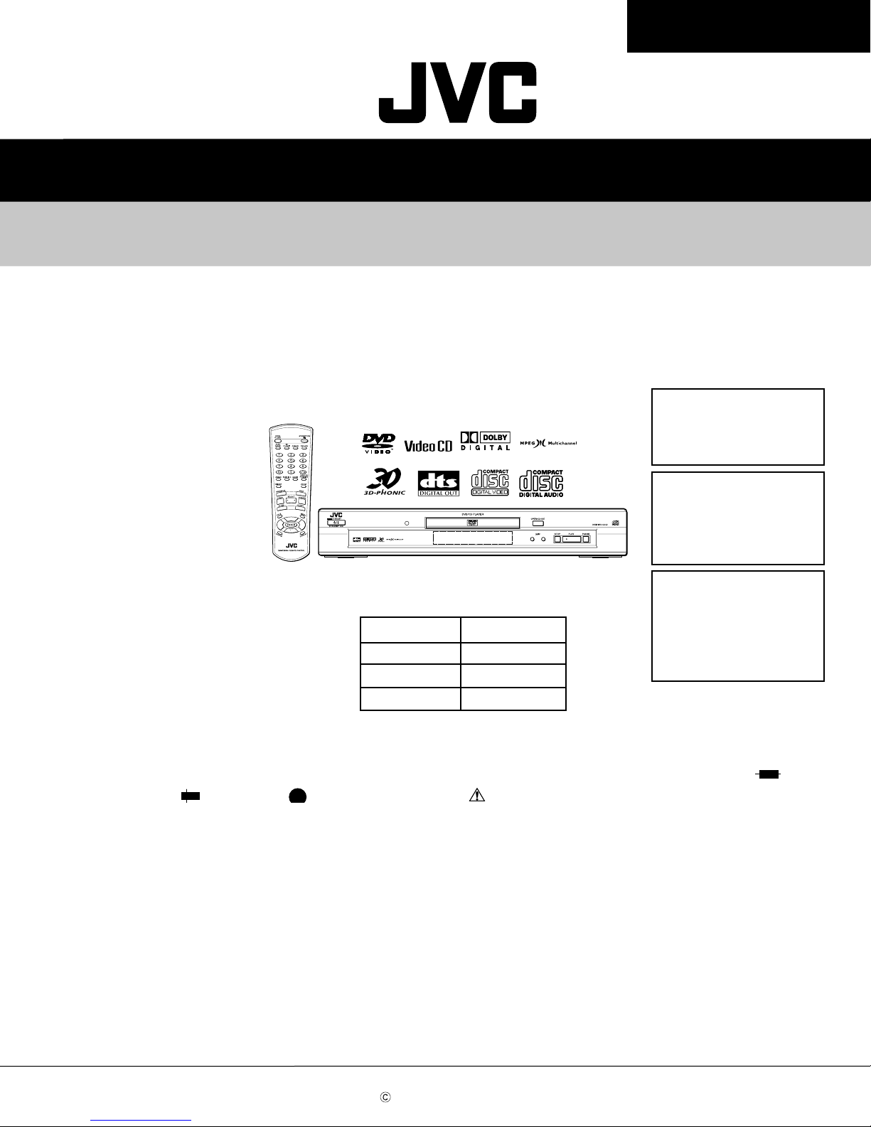
JVC XV-S40BK User manual

SERVICE MANUAL
DVD VIDEO PLAYER
No.A0006
Apr. 2001
COPYRIGHT 2001 VICTOR COMPANY OF JAPAN, LTD.
XV-S40BK / XV-S42SL
XV-E100SL
XV-S40BK/XV-S42SL
XV-E100SL
Area Suffix (XV-S42SL)
B ------------------------- U.K.
E --- Continental Europe
EN ---- Northern Europe
EV ------ Eastern Europe
Area Suffix(XV-E100SL)
B ------------------------- U.K.
E --- Continental Europe
EN ---- Northern Europe
EV ------ Eastern Europe
EE -- Russian Federation
B ------------------------- U.K.
E --- Continental Europe
EN ---- Northern Europe
Area Suffix (XV-S40BK)
This service manual is printed on 100% recycled paper.
Contents
Safety precautions ------------------------ 1-2
Preventing static electricity ------------- 1-3
Precautions for service ------------------ 1-4
Important for laser products ----------- 1-5
Disassembly method -------------------- 1-6
Adjustment method ---------------------- 1-15
Description of major ICs ---------------- 1-21
Model
XV-S40BK
XV-S42SL
XV-E100SL
Body color
Black
Silver
Silver
Each difference point
In regard with component parts appearing on the silk-screen printed side (parts side) of
the PWB diagrams, the parts that are printed over with black such as the resistor ( ),
diode ( ) and ICP ( ) or identified by the " " mark nearby are critical for safety.
When replacing them, be sure to use the parts of the same type and rating as specified
by the manufacturer. (Except the JC version)

2-1
XV-S40BK/XV-S42SL
XV-E100SL
FEP
(Front end processor)
IC101
4CH Driver
IC271
SPINDLE
MOTOR
DRIVER
IC251
ODC
(Optical disc controller)
IC301
IC311
ZIVA WAIT
OSCI/O
X401
EPROM
IC403
Unit CPU
IC401
ADSC
(Digital servo controller)
IC201
16M ROM
IC402
CN101
CN502CN503
T1CD T2CD F1CD F2CD
TR TC TD TA F2DVD F1DVD
T+ T-
F+ F-
TDOFS FODRV
TRDRV TRSDRV
BDO OFTR TGBAL
TBAL TE RFENV
FBAL FE TG AS
ARF+ ARF-
TESTSG JLINE
FEPEN CPSCK SDOUT SLEEP
CDDET1
CDDET2
PLLOK
DAT0~3
ADSCEN
CIRCEN
CPSCK
SDOUT
ADSCIRQ
/WR
/RD
/WR
/RD
STD0~7
WAITODC
WAITDEC
WAIT
DECIRQ
CPUA1~20
CPUD0~7 CPUA0~2
LSIRST
AV DECODER
IC501
27MHz
IC502
IC503
16M SDRAM
IC505
16M SDRAM
IC504
SYSCLK
DA-IEC
C/R/V
Y/B/U
CVBS/G/Y
CVBS
DA_DATA1
TO CN701
SHEET 4
TO CN961
SHEET 2
FROM
EXL-V7-1
FROM
EXL-V7-1
FROM
FLM-J1-1
LVB10226-A1
CPUD0~7
EPDO
EPDI
EPSK
EPCS
TX
85
IC312
59
60
IC321
IC322
CPUD0~7 CPUA0~17
U2SDT S2UDT
SCLKO REQ
BUSY
CPURST
CN201 CN202
V+5V
Block diagrams
DVD Servo control & AV decoder section(SHEET 5,6)
FM+
FM-
LM+
LM-
VH
SM1~3
H1+~H3+
H1-~H3-
SBRK SPMUTE
FG
DRVMUTE
SWOPEN SWUPDN

2-2
XV-S40BK/XV-S42SL
XV-E100SL
TO FW801
SHEET 1
TO FW802
SHEET 1
TO CN503
SHEET 6
SYSTEM
CONTROLLER
IC701
RESET
IC702
OSC
X701(8MHz)
DAC
IC703
DAC
CONTROL
LPF
IC741,IC751
OPTICAL
DIGITAL OUT
J703
ANALOG
AUDIO OUT
MUTE
Q791
Q743,Q753
Q744, Q754
D791,D792
MUTE
OPTICAL
DIGITAL OUT
-12V
+12V
TO SHEET 2
TO SHEET 3
CN703CN702CN701
LEA10016-A1
P.MUTE
RESET
POWERSW
STANDBYIND
REMO
AIN0
AIN2
DA_DATA1
U2SDT
S2UDT
SCLK
REQ
BUSY
CPURST
SWOPEN
SWUPDN
B5V
TX
J702 AV
COMPULINK
AV
COMPULINK
Q709
AVCI, AVCO
AUDIO_R
AUDIO_L
IC704
D3.3V
COAXIAL
DIGITAL OUT
System control & audio output section(SHEET 4)
FL Display & Operation switch section(SHEET 1)
S1~S24
1G~13G
TO SHEET 1
OUT1C
OUT1D
OUT2C
OUT2D
FL DISPLAY
DI801
TO SHEET 4
TO SHEET 2
S1~S24
1G~13G
B5V F- F+
OPERATION
SWITCH
S831~S835
S821
AIN0
AIN2
TO CN703
SHEET 4
FW801
REMOTE
CONTROL
IC801
POWER
SWITCH
S801
STANDBY
INDICATOR
D801
REMO
TO CN702
SHEET 4
FW802
POWERSW
STANDBYIND
FW803
Rch
Lch

2-3
XV-S40BK/XV-S42SL
XV-E100SL
LINE FILTER
L901 AC-DC
D901
SWITCHING
REGULATOR
IC901
AC-DC
D904
C914
AC-DC
D908
D910
TRANSFORMER
T901
FEED BACK
PC901 Q991
MODE SW.
PC902
AC-DC
D956
C982,C984
L957
AC-DC
D957
C987,C989
L959
MUTE DETECTION
D972,D973
Q966
C995,C996
AC-DC
D954
C979,C997
L955
AC-DC
D953
C965,C966
L952
AC-DC
D952
C963,C964
L951
AC-DC
D951
C960
-30V REG.
Q953
D950
+5V REG.
IC953
+5V REG.
IC951
+3.3V REG.
Q964,Q965
FL ON/OFF
Q951,Q952
CN961
F+
F-
-VDISP
B5V
TO SHEET 1
D5V
B5V
P.ON
+12V
P.MUTE
-12V
AC IN
LEA10016-A1
TO CN502
SHEET 6
M9V
D3.3V
TO SHEET 4
TO SHEET 3
DC Regulator section (SHEET 2)
CVBS
SVBS/Y/G
Y/Pb/B
C/Pr/R

2-4
XV-S40BK/XV-S42SL
XV-E100SL
J691
J603
J602
LVA10016-A1
C/Pr/R
Y/Pb/B
CVBS/Y/G
LPF
L601, L602
LPF
L611, L612
LPF
L621, L622
LPF
L631, L632
R/C
B
G
Lch
Rch
Y/COMPOSITE
TO SHEET 2
TO SHEET 4
CVBS Q631
Q621
COMPOSITE
Y/C SWITCH
S691
Q601
Q611
Audio & Video signal output section(SHEET 3)
S-VIDEO OUT
COMPOSITE
VIDEO OUT
AUDIO_L
AUDIO_R
T701
DOUT
L
RAUDIO OUT
COAXIAL
DIGITAL OUT
Lch
Rch

2-5
I
HA BC DE FG
1
2
3
4
5
6
XV-S40BK/XV-S42SL
XV-E100SL
S831
C821
D801 S821
IC801
C801
C802
R801
S833
S832
S834
S835
S801
FW802 FW801
FW803
FW803
R845R847 R846R848
4.7/50
SLR-342VC-T
GP1U271X
0.1
47/10
330
QSW0651-001Z
QUM125-09DGZ4 QUM123-11DGZ4
QUM123-12Z4Z4
QUM123-12Z4Z4
4301.1K 6802.2K
B5V
F-
F+
S2
S3
S4
S5
S1
S7
S13
S17
S18
S19
6G
S11
S12
S15
S21
S6
S8
S9
S14
S16
1G
2G
3G
4G
5G
7G
8G
9G
10G
S10
11G
12G
S22
13G
S24
S23
S20
FL Display & operation switch section
TO SHEET 4
TO SHEET 2
Standard schematic diagrams

2-6
I
HA BC DE FG
1
2
3
4
5
6
XV-S40BK/XV-S42SL
XV-E100SL
XV-S40BK/XV-S42SL
XV-E100SL
Parts are safety assurance parts.
When replacing those parts make
sure to use the specified one. Video signal
TO SHEET 4
TO SHEET 3
TO SHEET 1
Power supply section
Q953
P901
EP951
F901
D901
C906
L901
C907
R901
D902
C908
D903
Q966
C909
PC902
IC901
R903
K902 R904
R906 D910
C918
C914
C913
D904
D911
C905
C910C915
R900
D953
R908
R907
D908
PC901
C916
D951
C951
D952
C952
C953
D954
C954
C960 C961
Q951
R952
R953
D960
L951
C964 R955 Q952
C963
R954
IC951
C965
L952
C966 C967 C968C969
R972
C973
R971
IC953
C979 C997
L955
C981
R956
C984
C970
C982
D956
C956
L957
L959
C989C987
D957
C957
C992
Q991
R960
C993
D991
R969
C917
CP951
T901
D970
D972
D973 D974
R975
R973
R976
C995 C996
Q964
Q965
C902
CP952
R905
R911R910
C962
R980
D950
R961
R962
R963
R964
R965
C976
C994
C977
C978
R974
CN961
KTA1267/G/-T
S1WB/A/60-4101
0.001/AC250V
QQR1105-001 68K
F1T4-T2
0.0033/1K
F1T4-T2
KTA1267/G/-T
100p/1k
PC123Y02
STR-G6651
27
2.2k
680 F1T4-T2
0.1
39/25
100p/1k
F1T4-T2
1SS133-T2
220P470P
220
FMB-24
3.3K
0.47
F1T4-T2
PC123Y02
0.0033/AC250V
F1T4-T2
100p
F1T4-T2
100p
100p
F1T4-T2
100p
82/10 0.1
KTD863/Y/-T
10k
10K
MTZJ4.7B-T2
0.22
22/50 22k KRA104S-X
39/50
10
PQ05RD21
1000/10
22
470/10 0.1 0.1220/10
1.2k
100/10
3.9k
NJM78M05FA
820/16 220/16
22
0.1
12
220/25
0.1
560/25
F1T4-T2
100p
10
10
100/25180/25
F1T4-T2
100p
0.47/50
KTC3199/Y/-T
100
100p
MTZJ5.1C-T2
220
0.1
ICP-N10-T
QQS0097-001
1SS133-T2
1SS133-T2
1SS133-T2 1SS133-T2
5.6k
1K
220
220/16 22/16
2SB1184/QR/-X
KTC3199/Y/-T
0.068/AC250V
ICP-N5-T
68k
750K750K
22/50
1.5k
MTZJ36C-T2
680
1M
100
1M
10k
0.1
0.022/25
0.1
100/10
5.6K
QGB2027M8-26
P.MUTE
+12V
P.ON
C/Pr/R
CVBS
CVBS/Y/G
-12V
F+
Y/Pb/B
B5V
F-
CVBS
-VDISP
CVBS/Y/G
Y/Pb/B
C/Pr/R
D5V

2-7
I
HA BC DE FG
1
2
3
4
5
6
XV-S40BK/XV-S42SL
XV-E100SL
Video signal
Audio signal
TO SHEET 2
TO SHEET 4
Audio / video signal output section
K604
Q692
R611
R601
Q693
R615
R605
Q611
Q601
C639
C696
C697
C619
C609
R619
R609 J601
C691
K605
L602
J691
S691
R686
R685
C694
R694
C695
R695
Q691
R696
J603
C659 R659
R687
L601
R649
C649
C1704
R639
R629
C629
R688
J604
R602
L612L611
R612
C1703 R1723
Q696
Q697
R681
R682
R661
K708
R663
R664
T701
R665
R631
R635
Q631
L632L631
R632
R621
R625
Q621
L622L621
R622
Q694
R1732
C985
R1731
J602
D629
D639
R660
R603
R613
R661
R614
R604
R616 R606
C614
D609D619
C604
C686C685
R697
R698
C603
C601
C613
C611
R633
R634
R636
C634
C633
C631
R623
R624
R650
C624
C623
C621
NQR0227-004X
KRC102S-X
150
150
KRA102S-X
220
220
KTA1267/G/-T
KTA1267/G/-T
0.1/16
470/6.3
470/6.3
470/6.3
470/6.3
82
82 QNN0387-001
100p
NQR0227-004X
2.2
QNZ0516-001
QSW0454-001
150 150
470/6.3
68
470/6.3
68
KRC102S-X
0
470/6.3 68
68
5.6
QND0086-001
68470/6.3
220p
68
68
470/6.3
68
QNZ0499-001
0
2.25.6
0
150p
27
KRA102S-X
KRC102S-X
150
NI
10k
NQR0227-004X
10k
9.1k
QQR1185-001
2.2k
150
220
KTA1267/G/-T
2.25.6
0
150
220
KTA1267/G/-T
2.25.6
0
KRC102S-X
10
220/16
1k
QNN0361-001
1SS133-T2
1SS133-T2
10K
150
150
2.2K
0
0
560 560
47p
1SS133-T21SS133-T2
47p
470P470P
1k
100k
220p
470p
220p
470p
150
0
560
47p
220p
470p
150
0
560
47p
220p
470p
DOUT
RGBSEL
VS3
Lch
NTSC/PAL
AUDIO_L
AUDIO_R
Rch
C/Pr/R
Y/Pb/B
D5V
+12V
VS1
CVBS/Y/G
CVBS

2-8
I
HA BC DE FG
1
2
3
4
5
6
XV-S40BK/XV-S42SL
XV-E100SL
XV-S40BK/XV-S42SL
XV-E100SL
Audio signal
TO
SHEET 3
TO
SHEET 1
TO
SHEET 2
System control & audio signal DAC section
Q709
IC701
R1709
EP711
R795
R1707
R780
R706
K706
R1713
IC703
C715
C716
R1725
C721
C714
R713R715
R723
R724
R725
C717
C718
C711
R721
R1726
RA701
R728
R729
R744
R743
R742
R746
R745
IC741
C741
R1730
R1729
RA703
R748 R761 IC741
R762
R783
R764
C745 R782
R754
R753
R752
R756
R755
IC751
C751
K702
IC791
C735
R1711
R758 R771
IC751
R772
R793
R774
C755
R792
R1728
J702
R1716
R731
C731
RA702
R790
R781
R791
C737
C738
C704
C797
R797 Q791 D791
D792
C746
R766
R765
C747
Q743 R768
R767
C756
R776
R775
C757
Q753 R778
R777
J703
R705
C707 C736
C729
C713
R707
R1710
R1708
L710
Q744
C728
C705
C706
R703
R1704
X701
L709R708
IC702
R704
R788
R763
R773
C749
C739
Q754
R769
R779
R1714
R1722
C1701 C1702
D702
IC704
K705
C724
C722
R717
C708
R711
R1727
R741
R740
C740
C742
R747
CN703
C744
C761
C762
R751
R750
C750
C752
R757
C754
C771
C772
C730
K703
K701
R1724
R786
R709
D709
R789
R702
C702
K704
C709
R701
C701
D701
R1715
CN702
R1721
CN701
KRC107S-X
MN101C35D*
1K4.7K
2.2k
1.1K
100K
NQR0227-004X
100
MN35505-X
NI
1000/6.3
1k
NI
1000/6.3
2222
470
470
470
1.5
470/6.3
1.5
470
NI
NI
470
470
3.6k
18k
18k
3.3k
18K
NJM4580M-X
220p
10k
2.2k
NI
1.1k 1.1k NJM4580M-X
680
220
18K
0.01
220
3.6k
18k
18k
3.3k
18K
NJM4580M-X
220p
10
NI
NI
NI
1.1k 1.1k
NJM4580M-X
680
220
18K
0.01
220
2.2k
QNS0089-001
1k
3.3k
0.01
NI
1.1K
1.1K
1.1K
22/25
22/25
0.1
0.0015
47K KRA102S-X 1SS133-T2
1SS133-T2
22/25
27K
560
2200p
2SD2144S/VW/-T
10K
100
22/25
27K
560
2200p
2SD2144S/VW/-T
10K
100
QNZ0487-001
2.2
100/6.3 0.1
NI
470p
NI
1K
2.2k
NI
2SD2144S/VW/-T
100/10
0.1
0.1
1M
1k
QAX0667-001Z
2.2100
IC-PST9140-T
1K
NI
3.6k
3.6k
NI
NI
2SD2144S/VW/-T
10k
10k
4.7K
75
47/25 47/25
MTZJ3.3B-T2
TC7S08F-W
NQR0227-004X
NI
NI
10
NI
10
0
27k
27k
1000p
0.033
3.6K
QGD2501C1-03Z
680p
100/16
100/16
27k
27k
1000p
0.033
3.6K
680p
100/16
100/16
0.22
NQR0227-004X
NQR0227-004X
100
33K
10k
1SS133-T2
0
4.7k
0.1
NQR0227-004X
330P
1K
1/50
1SS133-T2
10k
QGD2501C1-05Z
330
QGB2027M8-26
DA_BCK
DA_BCK
DA_LRCK
DCLK
DAC0CS
1G
2G
SK
DA_DATA1
REMO
DA_LRCK
DA_DATA1
RGBSEL
POWER_SW
DDATA
SWOPEN
SWUPDN
CPURST
DGND
DCLK
P.MUTE
AUDIO_L
NTSC/PAL
+12V
DDATA
AUDIO_R
DI
D5V
BUSY
REQ
DAC0CS
B5V
DOUT
Lch
Rch
A.GND
-12V
S14
U2SDT
S15
S16
S17
S18
S19
S20
S21
S22
SCLKO
S23
S24
3G
4G
5G
6G
7G
8G
9G
10G
S2UDT
11G
12G
13G
VS3
VS1
CS
DI
DO
CS DO
SK
P.ON
/LMMUTE
TCLOSE
TOPEN
AVCO
S2
AVCO
AVCI
BUSY
SCLK
U2SDT
S2UDT
REQ
SWUPDN
SWOPEN
/LMMUTE
TOPEN
CPURST
S3
S4
S5
S6
S7
S8
S9
S10
S11
S12
S13
S1
-VDISP
TCLOSE
AVCI

2-9
I
HA BC DE FG
1
2
3
4
5
6
XV-S40BK/XV-S42SL
XV-E100SL
Digital data signal
TO SHEET 6TO SHEET 6
DVD Servo control section
R111
R289
IC201
R288
C287
R208
C105
IC271
IC301
IC251
C106
TP304
C274
IC101
IC102
CN201
CN202
C109
C102
C271
R121
R122
R123
R124
CN101
R108
C239
R110
R112
C240
R109
C151
R114R113
R292 R293
C131
C288
R125
C145
C146
C222
C201
C136
C135
C134
C133
C132
R129
R128
R127 C130
TP568
C272
C273
R209
R210
R206
R280
C241
TP140
C208
C209
C210
R211
R212 C231
IC403
C412
C232
C233
R347
TP158
TP141
C402
R215
R412
R413
R282
C223
R281
C280
C225
R218
TP202
C226
C230
C227
C228
R219
R118
C224
C122
R285
R117
C314
C315
C120
R116
C312
C121
R154
C325
R155
TP119
R317
X301
R284
C313
R283
TP118
TP117
TP116
TP122
C242
R318
C281
R286
C103
TP205
C260
C261
C262 C263
TP415
R152
R251
R252
R153
C251
C252
TP105
C254
C248
C249
D301
TP307
C311
C214
R255
C229
C256
R271
R256
R277R276
C276
C275 R275
R274
R273
R278
R279
IC401
C406
C401
R409
R403
TP101
TP136
R316
TP303
TP103
R348
R419
R234
R233
C407
R416
R415
R414
R350
TP305
R301
R417
D271
R408
R232
C283
TP148
C284
TP176
TP212
R302
TP139
R245
R246
TP425
C218
R243
R242
C213
TP570
TP207
TP175
TP201
TP206
R303
C215
C217
C219
C216
C220
TP149
IC321
R202
R290
R203
TP306
R204
R205
R349
R291
R259
R304
R305
TP170
R306
TP174
TP167
C212
TP169
TP102
R307
R308
R309
TP567
C304
C305
C303
C302
C301
C408
R411
TP405
TP232
R332
C413 C414
TP302
TP401
K102
TP213
K201
TP138
K202
R221
K203
R222
TP137
TP135
TP134
IC312IC311
TP133
TP132
TP131
C342
C341
R341
R342
TP156 TP154
R343
K402
C324
C317
TP301
TP173
TP164
TP166
R404
R405
Q101
R258
Q102
R287
R106
R104
TP16
R107
TP17
R105
C207
TP162
C405
R103
Q104
R102
R101
C206
C108
C107
C104
R147
C101
TP127
C152
C117
R272
TP128
C116
C115
C110
C286
C118
C119
R115
R131
R132
C144
C264
C221
C141
C140
R226
C138
C139
C127
TP129
C124
C160
C205
R231
R236
TP142
C137
C123 C143
C161
C129
TP143
TP144
C128
R214
C211
R213
R331
TP153
TP155
TP151
C126
TP145
TP146
TP208
C125
TP126
TP210
TP203
TP224
R220
R248
TP125
R363
R223
TP124
TP123
C159
R227
C244
C245
IC202
C320
C321
TP121
R119
C306
TP120
TP115
C319
R320
X401
TP114
TP113
TP112
R225
C282
TP111
TP110
TP106
R165
TP107
TP109
TP108
C257
R166
TP204
C258
C259
C326
R228
R229
C253
R254
R230
R253
C327
TP18
R345
R321
R322
R323
R324 R325
R326
R327
R330
C255
C246
R346
C278
TP220
Q105
C279
C318
R428
R427
R426
R425
R424
R423
R422
C307
C309
C310
C277
C409
TP211
TP231
TP19
TP20
TP8
TP214
TP215
R235
R257
TP9
TP10
TP11
TP12
TP13
TP217
TP216
TP14
C247
TP218
R249
TP15
TP1
TP2
TP3
C410
TP413
R250
C158
TP219
R329
TP152
TP4
C237
C238
R241
R240
R239
R238
R237
TP5
TP6
TP221
TP7
R421
C202
R207
C203
C204
C345
C346
TP150
R310
R311
R418
R407
R364
TP161
TP233
TP234
TP225
TP226
R224
K301
K303
K302
K103
TP159
TP157
IC322
C343
C344
R312
C316
R328
TP160
TP163
NI
7.5k
MN67706ZY
0
0.1/16
47k
47/6.3
BA5983FM-X
MN103S13BDA
BA6664FM-X
47/6.3
0.1/16
AN8702FH
MM3022JN-X
QGF1016F2-15W
QGF1016F2-06W
0.1/16
NI
D5V
22/6.3
0
00
0
QGF0501F2-30X
18k
0.018/16
27k
27k
D.GND
47p
NI
22/6.3
1k6.8k
S5V
10K 9.1k
12p
1/50
NQR0265-003X
0.01/16
NI
0.1/16
0.47/16
D5V
0.047/16
0.027/16
560p
560p
0.1/16
1M
1M
2.2k
0.1/16
M9V
NI
0.1/16
12k
47k
4.7
M.GND
2.4k
0.01/16
0.1/16
0.001
0.001
27k
27k 0.0056/25
BR93LC66F-X
0.1/16
0.001
D.GND
0.1/16
1k
D2.7V
0.1/16
1M
10k
4.7k
10k
0.1/16
2.4k
NI
1/16
15k
NI
NI
0.001
0.001
47k
30k
0.1/16
180p
10k
12k
0.1/16
0.1/16
82p
68k
18p
22p
NI
NI
0
0
NAX0375-001X
10k
18p
10k
1/16
0
0.022
9.1k
NI
0.1/16
0.1/16
0.1/16 0.1/16
1
1
3.3
4.7
0.1/16
22/16
22/6.3
M9V
M.GND
0.15/16
0.1/16
NI
D.GND
D5V
0.1/16
0.1/16
10k
0.1/16
0.1/16
47
47
12k12k
NI270p
10k
10k
0
10k
10k
MN102L25G*
D.GND
0.1/16
0.1/16
NI
4.7k
1M
1k
NI
4.7k
4.7k
0.1/16
4.7k
4.7k
4.7k
1k
D5V
47k
4.7k
NI
4.7k
4.7k
NI NI
47k
S3V
1k
1k
0.1/16
1k
1k
0.1/16
D2.7V
D3V
47k
S3V
D.GND
S.GND
33/6.3
100/6.3
100/6.3
1/16
1/16
TC7WH74FU-X
S.GND
47k
7.5k
47k
47k
47k
1k
6.8k
10k
47k
47k
47k
0.1/16
47k
47k
10k
0.1/16
0.1/16
0.1/16
0.1/16
0.1/16
22/6.3
4.7k
NI
NI NI
NQR0007-002X
NQR0007-002X
NQR0007-002X
NI
NQR0007-002X
NI S3V
TC7SH32FU-XTC7SH08FU-X
D.GND
0.1/16
0.1/16
NI
0
1k
NQR0007-002X
0.1/16
D5V
D3V
1/16
NI
D.GND
4.7k
KTA1001/Y/-X
0
KTA1001/Y/-X
NI
2.2
27
2.2
27
470p
0.1/16
33k
NI
33k
10k
270p
0.1/16
0.1/16
0.1/16
0
0.1/16
15/6.3
NI
1
NI
NI
NI
1/50
0.15/16
220p
24k
8.2k
10k
0.1/16
0.01/16
560P
0.1/16
22/6.3
12k
0.1/16
0.1/16
0.001
0.1/16
0.1/16
120p
0
0
NI
0.1/16
0.1/16
33/4
NI
0.1/16
12k
NI
5.6k
NI
56/6.3
0.1/16
47k
47k
NI
47k
0.1/16
1k
0.1/16
0.01/16
TC7WT125FU-X
0.1/16
0.1/16
NI
0.1/16
0.1/16
NI
NAX0331-001X
6.8k
0.01/16
0
0.01/16
1.8k
0.01/16
0.01/16
0.1/16
18k
27k
0.1/16
20k
27k
NI
100/4
5.6k
NI
47k
NI
47k
NI
NI
NI
NI
0.022
0.1/16
4.7k
0.001
NI
NI
0.1/16
*
*
*
*
*
*
*
0.1/16
0.1/16
0.1/16
0.001
0.1/16
0
1
0.1/16
47k
0.1/16
47k
NI
NI
0.1/16
0.1/16
220
220
220
220
220
*
560p
NI
560p
330p
100/6.3
1/16
1k
1k
4.7k
NI
0
0
NQR0007-002X
NQR0007-002X
NQR0007-002X
NQR0007-002X
TC74VHC00FT-X
0.1/16
0.1/16
1k
100/4
47k
CPDET1
CIRCEN
ADSCEN
TGBAL
CPDET2
AS
TE
/WR
FE
TBAL
TRDRV
IPFLAG
NTRON
PLLOK
LG
SYSCLK
SLEEP
LDCUR
FEPEN
CPSCK
SDOUT
T2CD
F2CD
FBAL
T1CD
STD7
FODRV
STD6
CPURST
STD5
STD4
STD3
STD2
STD1
STD0
STEN
JLINE
F1CD
TB
ODCIRQ2
ODCIRQ
TC
EPDI
CSROM
EPDOEPCS
EPSK
SLEEP
ARF+
SCLKO
S2UDT
U2SDT
BUSY
REQ
ADSCIRQ
SDOUT
SDIN
CPSCK
ARF-
FEPEN
DECIRQ
LSIRST
EPDO
EPDI
EPSK
EPCS
CPUA0
CPUA1
CPUA2
CPUA3
TD
TA
RFENV
BDO
TXSEL
/RD
/WR
OFTR
/DRVMUTE
F2DVD
F1DVD
RF-
T+
F+
F-
T-
HAGUP
RF+
SYSCLK
IPFLAG
NTRON
LG
JMPINH
PLLOK
SDIN
CPDET1
CPDET2
NCLOCK
SUBC
LDCUR
TRSDRV
TG
RFENV
ADSCTX
TESTSG
JMPINH
BDO
LM-
LM+
FM+
FM-
SM1
SM2
SM3
H1+
H1-
H2+
H2-
H3+
H3-
VH
FG
TRVSW
SWOPEN
SWUPDN
SPDRV
/RD
WAITDEC
CSDEC
CPUD2
CPUD3
CPUD4
CPUD5
CPUD6
CPUD7
CPUA17
CPUA16
CPUA15
CPUA14
CPUA13
CPUA12
CPUA11
CPUA10
CPUA9
CPUA8
CPUA7
CPUA6
CPUA5
CPUA4
CPUA3
CPUA2
CPUA1
CPUA0
/WR
/RD
CPUD1
CPUD0
/DRVMUTE
RF-
FG
TRVSW
TA
F1DVD
F2DVD
F1CD
F2CD
TD
DAT0
DAT1
DAT2
DAT3
CHCK40
NCLOCK
SUBC
TB
TOPEN
HMFON
TC
STCLK
STVALID
SBRK
T-
T+
F+
F-
/LMMUTE
/SPMUTE
SBRK
T2CD
T1CD
/SPMUTE
TCLOSE
ODCIRQ2
ODCIRQ
RF+
TE
HAGUP
CPUD0
CPUD1
CPUD2
CPUD3
CPUD4
CPUD5
CPUD6
CPUD7
TESTSG
HMFON
CPUA4
CPUA5
CPUA6
CPUA7
CPUA8
CPUA9
CPUA10
CPUA11
CPUA12
CPUA13
CPUA14
CPUA15
CPUA16
CPUA17
CPUA18
CPUA19
CPUA20
SPDRV
OFTR
TGBAL
TBAL
BDO
FBAL
JLINE
ARF+
ARF-
AS
TRSDRV
TG
ADSCIRQ
CHCK40
FE
DAT3
DAT2
DAT1
DAT0
ADSCEN
CIRCEN
CPSCK
SDOUT
H3-
H3+
H2-
H2+
H1-
H1+
LM+
LM-
FM+
FM-
SM1
SM2
SM3
VH

2-10
I
HA BC DE FG
1
2
3
4
5
6
XV-S40BK/XV-S42SL
XV-E100SL
XV-S40BK/XV-S42SL
XV-E100SL
Audio signalDigital data signal Video signal
TO
SHEET 5
TO
SHEET 5
AV Decoder section
C543
IC501
C556
C557
R559
D501
R530
R588
K506
CN502
L1
R546
R551
R558
R549
R582
R585
R584
Q1
C17
R1
C542
IC1
C561 C562
C566
R552
C16
C15
C547
R571
C567
IC402
R553
R554
C541
C540
IC504
C411
R432
K401
R583:
R581
R586
R587
CN503
C571
R594
R595
R596
R597
R598
R599
R555
C534
K502
C539
R528
TP507
R501
R548
C531
R556
R557
R502
C516
C501
C502
C503
C504
C505
C506
C507
R523
C525
C518
R524
R525
R526
R527
R529
TP505
R531
K501
C532
TP506
C517
C527
IC505
C536
C535
R550
C11
C13
TP47
C2
C1
TP66
C14
R510
C4
C6
C12
C10
C9
C8
C7
TP94
TP93
TP92
C3
C5
TP91
D551
D552
R509
C544
TP43
TP38
TP39
TP40
TP41
TP42
K505
TP45
K504
TP44
R431
IC503
C568
C569
C570
C533
R533
R545
R534
R535
R536
R537
R538
C530
R539
R547
R540
C515
C514
C513
C512
C511
C510
C509
C508
C529
C528
C526
C524
C523
C522
C521
C520
C519
R532
K503
R504
R506
C538
C537
R507
R508
R511
R512
R513
R514
R515
R516
R522
R521
R520
R519
R518
R517
IC502
TP48
TP50
TP49
TP52
TP54
R543
R542
R541
TP55
TP56
TP57
TP59
TP61
TP63
TP65
TP67
TP68
TP69
TP70
TP71
TP72
TP73
0.1/16
ZIVA-4.1-PA2
100/6.3
0.1/16
NI
1SR154-400-X
NI
NI
NQR0007-002X
QGB2027L1-26X
S5V
D3V
D5V
NQL044K-100X
180
NQR0007-002X
M.GND
NI
0
D2.7V
M9V
NI
NI
NI
KTC4377/C/-X
0.1/16
10
Z3V
22/6.3
MM3023DN-X
S.GND
0.1/16 22/6.3
0.1/16
0
V.GND
D.GND
33/4
0.1/16
D5V
0.1/16
NI
D.GND
S3V
22/6.3
K3N5C1000D-J*
NI
NQR0007-002X
0.1/16
22/6.3
KM416S1120DT-G8
D.GND
D.GND
0.1/16
4.7k
D5V NQR0007-002X
NI
D.GND
NQR0007-002X
NI
NI
QGB2027L1-26X
NI
NI
NI
NI
NI
NI
NI
NQR0007-002X
100/6.3
NQR0007-002X
Z3V
D.GND
0.1/16
1k
D.GND
1k
3.3k
0.1/16
NQR0007-002X
0
D.GND
4.7k
0.1/16
0.1/16
0.1/16
0.1/16
0.1/16
0.1/16
0.1/16
0.1/16
NI
0.1/16
0.1/16
180
NI
NI
180
180
Z3V
D.GND
33
NQR0007-002X
0.1/16
0.1/16
0.1/16
KM416S1120DT-G8
0.01/16
0.1/16
NI
100/6.3
NI
22/6.3
0.1/16
NI
33
0.1/16
0.1/16
0.1/16
NI
NI
NI
NI
22/6.3
22/6.3
NI
NI
33
0.1/16
NQR0269-001X
NQR0201-001X
4.7k
TC74VHC00FT-X
NI
NI
NI
0.1/16
33
4.7k
33
33
33
33
33
100/6.3
33
2.2k
33
Z3V
0.1/16
0.1/16
0.1/16
0.1/16
0.1/16
0.1/16
0.1/16
0.1/16
0.1/16
0.1/16
0.1/16
0.1/16
0.1/16
0.1/16
0.1/16
0.1/16
0.1/16
1k
NQR0007-002X
33
33
0.1/16
22/6.3
33
33
33
33
33
33
33
33
33
33
33
33
33
33
NAX0393-001X
0
0
0
V3V
C/R/V
CVBS/G/Y
DA_XCK
DA_XCK
BUSY
DA_LRCK
CVBS
Y/B/U
DA_BCK
DA_DATA0
DA_DATA2
DA_DATA1
DA_DATA3
U2SDT
/LMMUTE
SD-CS0
CPURST
S2UDT
M9V
REQ
SCLKO
D3V
D5V
/RD
/WR
Z3V
LSIRST
DA_BCK
TOPEN
TX
CPUA20
CPUA9
LDQM
LDQM
SD-CS1
DA_LRCK
DA_DATA0
DA_DATA1
DA_DATA2
DA_DATA3
CPUA11
CPUA12
CPUA13
CPUA14
CPUA16
CPUA17
CPUA0
CSDEC
CPUD4
CPUD6
CPUD7
V5V
C/R/V
Y/B/U
TCLOSE
CVBS/G/Y
CVBS
CPUA10
CPUD5
SWOPEN
SWUPDN
CPUA19
CPUA18
CPUA8
CPUA7
CPUA6
CPUA5
CPUA4
CPUA3
CPUA2
CPUA1
/RD
CPUD0
CPUD1
CPUD2
CPUD3
CPUA15
LDQM
/MWE
SD_CAS
SD_RAS
MA11
MA10
MA0
MA1
MA2
MA3
MD0
MD1
MD2
MD3
MD4
MD5
MD6
MD7
MA4
MA5
MA6
MA7
MA8
MA9
SD_CLK
MD8
MD9
MD10
MD11
MD12
MD13
MD14
MD15
WAITDEC
LDQM
/MWE
DECIRQ
SD_CAS
SD_RAS
MA11
MA10
MA0
MA1
MA2
MA3
MD0
MD1
MD2
MD3
MD4
MD5
MD6
MD7
MA4
MA5
MA6
MA7
MA8
MA9
SD_CLK
MD8
MD9
MD10
MD11
MD12
MD13
MD14
MD15
/MWE
STD2
STD1
CPUA0
CPUA1
CPUD7
CPUA2
CPUD6
CPUD5
CPUD4
CPUD3
CPUD2
CPUD1
CPUD0
LDQM
SD_CLK
SD_CAS
SD_RAS
MA9
MA8
MA7
SD-CS1
MA10
MA0
MA6
MA5
MA4
MA1
MA2
MA3
MA11
SD-CS0
STD0
STD3
STD4
STD5
STD6
STD7
STVALID
STEN
STCLK
CSROM
MD7
MD8
MD6
MD9
MD5
MD10
MD4
MD11
MD3
MD12
MD2
MD13
MD1
MD14
MD0
MD15
DECTX
ADSCTX
TXSEL

2-11
I
HA BC DE FG
1
2
3
4
5
6
XV-S40BK/XV-S42SL
XV-E100SL
Printed circuit boards
Main board
C601
C603
C604
C609
C611
C613
C614
C619
C621
C623
C624
C629
C631
C633
C634
C639
C649
C659
C685
C686
C691
C701
C702
C704
C705
C706
C707
C708
C709
C713
C714
C715
C716
C718
C722
C724
C728
C730
C735
C736
C737
C739
C740
C741
C742
C745
C746
C747
C751
C752
C754
C755
C756
C757
C762
C771
C772
C797
C821
C902
C906
C907
C908
C909
C910
C913
C914
C915
C917
C918
C931
C951
C952
C953
C954
C956
C957
C960
C961
C962
C963
C964
C965
C966
C967
C968
C969
C970
C973
C976
C977
C978
C979
C981
C982
C984
C987
C989
C992
C993
C994
C995
C996
C997
C1701
C1702
C1703
C1704
CN701
CN702
CN703
CN961
D619
D639
D701
D702
D709
D791
D792
D901
D902
D903
D904
D908
D910
D911
D950
D951
D952
D953
D954
D956
D957
D960
D970
D972
D973
D974
D991
EP951
FC901
IC701
IC702
IC703
IC704
IC741
IC751
IC791
Q693
IC901
IC951
IC953
Q696
K604
K701
K702
K703
K704
K705 K706
K708
K902
L709
L710
L901
L951
L952
L955
L957
L959
P901
PC901
PC902
Q601
Q611
Q621
Q631
Q697
Q709
Q743
Q753
Q791
Q951
Q952
Q953
Q964
Q965
Q966
Q991
R601
R602
R603
R604
R605
R606
R609
R611
R612
R613
R614
R615
R619
R621
R622
R623
R624
R625
R629
R631
R632
R633
R634
R635
R636
R639
R649
R659
R660
R661
R681
R682
R685
R686
R694
R695
R696
R697 R698
R701
R702
R703
R704
R705
R706
R707
R708
R709
R711
R713
R715
R717
R721
R723
R724
R725
R728
R729
R731
R740
R741
R742
R743
R744
R745
R746
R747
R748
R750
R751
R752
R753
R755
R756
R757
R758
R761
R762
R763
R764
R765
R766
R767
R768
R771
R772
R773
R774
R775
R776
R777
R778
R780
R781
R782
R783
R786
R788
R789
R790
R791
R792
R793
R795
R797
R900
R901
R903 R904
R905
R907
R908
R911
R952
R953
R954
R955
R956
R960 R961
R962
R963
R964
R965
R969
R971
R972
R973
R974
R975
R980
R1704
R1707
R1708
R1709
R1710
R1711
R1713
R1714
R1715
R1716
R1721
R1722
R1723
R1724
S691
C731
R1728
R1729
T901
X701
Q744
Q754
R769
R779
R1725
R1726
R1727
RA701 RA702 RA703
R688
R687
R663
R664
Q694
R662
R665
K605
FC902
C905
C904
HS901
C985
R1732
R1731
R699
[B7074]
T1B
C801
C802
D801
FW801
FW802
IC801
R845 R846 R847 R848
S801
S821
S831
S832
S833 S834S835
R801
FW803

2-12
I
HA BC DE FG
1
2
3
4
5
6
XV-S40BK/XV-S42SL
XV-E100SL
XV-S40BK/XV-S42SL
XV-E100SL
Forward side Reverse side
C1
C2C3
C5
C6
C11
C13
C14
C16
C17
C101
C102
C103
C104
C105
C106
C107 C108
C109
C121
C126
C128
C129
C131
C134
C140
C141
C143
C144
C145
C146
C151
C152
C158
C161
C202
C203
C204
C207
C213
C215
C217
C218
C219
C221
C227
C230
C231
C232
C239
C240
C241
C244
C245
C246
C252
C254
C256
C271
C272
C273
C274
C275C276
C277
C278
C279
C280
C281
C282
C283C284
C286
C287
C303
C304
C305
C312
C313
C316
C325
C327
C345
C346
C407
C408
C410
C411
C413 C414
C526
C530
C531
C532
C533
C534
C535
C536
C537
C538
C539
C540
C541
C542
C543
C556
C557
C561
C562
C566
C567
D271
D301
D501
D551
D552
IC201
IC271
IC301
IC401
IC503
IC504
IC505
K103
K201
K203
K301
K303
K401
K402
K501
K502
K503
K504
K505
K506
R550
R553 R555
K561
R582
R583
R584
R585
R586
R587
R588
R594
R595
R596
R597
R598
R599
L1
Q1
Q101
Q102
Q104
Q105
R1
R109 R117
R119
R121
R122
R125
R128
R131
R132
R147
R154
R166
R206
R207
R208
R215
R218
R220
R223
R227
R237
R238
R239
R240
R241
R242
R243
R245
R246
R248
R249
R250
R255
R256
R272
R273
R274
R275 R276
R277
R278R279
R280
R281
R282
R283
R284
R285
R286
R287
R288
R289
R290
R291 R301
R302
R303
R304
R305
R306
R307
R308
R309
R310
R311
R316
R320
R321
R322
R323
R325
R326
R327
R329
R330
R331
R332
R345
R346
R350
R363
R364
R407
R417
R421
R422
R423
R424
R425
R426
R427
R428
R431
R504
R506
R507
R508
R509
R510
R511
R512
R513
R514
R515
R516
R517
R518
R519
R520
R521
R522
R527
R529
R530
R547 R548
R558
X301
X401
R292
R293
C568
C569
C570
C4
C7
C8
C9
C10
C12
C15
C110
C115
C116
C117
C118
C119
C120
C122
C123
C124
C125
C127
C130
C132
C133
C135
C136
C137
C138
C139
C159
C160
C201
C205
C206
C208
C209
C210
C211
C212
C214
C216
C220
C222 C223
C224
C225
C226
C228
C229
C233
C237
C238
C242
C247
C248
C249
C251
C253
C255
C257
C258
C259
C260
C261
C262
C263
C301
C302
C306
C307C309
C310
C311
C314
C315
C317
C318
C319 C320
C321
C324
C326
C341
C342
C343
C344
C401
C402
C405
C406
C409
C412
C501
C502
C503
C504
C505
C506
C507
C508
C509
C510
C511
C512
C513
C514
C515
C516
C517
C518
C519
C520
C521
C522 C523
C524
C525
C527
C528
C529C544
C547
CN101
CN201
CN202
CN502
CN503
IC1
IC101
IC102
IC202
IC251
IC311
IC312
IC321
IC322
IC402
IC403
IC501
IC502
K102
K202
K302
R551
R554
R556
R557
R101
R102
R103
R104
R105
R106
R107
R108
R110
R111
R112 R113
R114
R115
R116
R118
R123
R124
R127
R129
R152R153
R155
R165
R202
R203
R204
R205
R209
R210
R211
R212R213
R214
R219
R221
R222
R224
R225
R226
R228
R229
R230
R231
R232
R233
R234
R235
R236
R251
R252
R253
R254
R257
R258
R259
R271
R312
R317
R318
R324
R328
R341R342
R343
R347
R348
R349
R403
R404
R405
R408
R409
R411 R412
R413
R414
R415
R416 R418
R419
R432
R501
R502
R523
R524 R525
R526 R528
R531
R532
R533
R534
R535
R536
R537
R538
R539
R540
R541
R542
R543
R545
R546
R559
R571
TP1
TP2
TP3
TP4
TP5
TP6
TP7
TP8
TP9
TP10
TP11
TP12
TP13
TP14
TP15
TP16
TP17
TP18
TP19
TP20
TP38
TP39
TP40
TP41
TP42
TP43
TP44
TP45
TP47
TP48
TP49
TP50
TP52
TP54
TP55
TP56
TP57
TP59
TP61
TP63
TP65
TP66
TP67
TP68
TP69
TP70
TP71
TP72
TP73
TP91
TP92
TP93
TP94
TP101
TP102
TP103
TP105
TP106
TP107
TP108
TP109
TP110
TP111
TP112 TP113
TP114
TP115
TP116
TP117
TP118
TP119
TP120
TP121
TP122
TP123
TP124
TP125
TP126
TP127
TP128
TP129
TP131
TP132
TP133
TP134
TP135
TP136
TP137
TP138
TP139
TP140
TP141
TP142
TP143
TP144
TP145
TP146
TP148
TP149
TP150
TP151
TP152 TP153
TP154
TP155
TP156 TP157
TP158
TP159
TP160
TP161
TP162
TP163
TP164
TP166
TP167
TP169
TP170
TP173
TP174
TP175
TP176
TP201
TP202
TP203
TP204
TP205
TP206
TP207
TP208
TP210
TP211
TP212
TP213
TP214
TP215
TP216
TP217
TP218
TP219
TP220
TP221
TP224
TP225
TP226
TP231
TP232
TP233
TP234
TP301
TP302TP303
TP304
TP305
TP306
TP307
TP401
TP405
TP413
TP415
TP425
TP505
TP506
TP507
TP567
TP568
TP570
C264
C288
C571
R549
DVD Servo control board

XV-S40BK/XV-S42SL/XV-E100SL
1-2
1. This design of this product contains special hardware and many circuits and components specially
for safety purposes. For continued protection, no changes should be made to the original design
unless authorized in writing by the manufacturer. Replacement parts must be identical to those
used in the original circuits. Services should be performed by qualified personnel only.
2. Alterations of the design or circuitry of the product should not be made. Any design alterations of
the product should not be made. Any design alterations or additions will void the warranty
and will further relieve the manufacture of responsibility for personal injury or property damage
resulting therefrom.
3. Many electrical and mechanical parts in the products have special safety-related characteristics.
These characteristics are often not evident from visual inspection nor can the protection afforded
by them necessarily be obtained by using replacement components rated for higher voltage,
wattage, etc. Replacement parts which have these special safety characteristics are identified in
the Parts List of Service Manual. Electrical components having such features are identified by
shading on the schematics and by ( ) on the Parts List in the Service Manual. The use of a
substitute replacement which does not have the same safety characteristics as the recommended
replacement parts shown in the Parts List of Service Manual may create shock, fire, or other
hazards.
4. The leads in the products are routed and dressed with ties, clamps, tubings, barriers and the
like to be separated from live parts, high temperature parts, moving parts and/or sharp edges
for the prevention of electric shock and fire hazard. When service is required, the original lead
routing and dress should be observed, and it should be confirmed that they have been returned
to normal, after reassembling.
5. Leakage current check (Electrical shock hazard testing)
After reassembling the product, always perform an isolation check on the exposed metal parts of
the product (antenna terminals, knobs, metal cabinet, screw heads, headphone jack, control
shafts, etc.) to be sure the product is safe to operate without danger of electrical shock.
Do not use a line isolation transformer during this check.
Plug the AC line cord directly into the AC outlet. Using a "Leakage Current Tester", measure
the leakage current from each exposed metal parts of the cabinet , particularly any exposed
metal part having a return path to the chassis, to a known good earth ground. Any leakage
current must not exceed 0.5mA AC (r.m.s.)
Alternate check method
Plug the AC line cord directly into the AC outlet. Use an AC voltmeter having, 1,000 ohms
per volt or more sensitivity in the following manner. Connect a 1,500 10W resistor paralleled by
a 0.15 F AC-type capacitor between an exposed
metal part and a known good earth ground.
Measure the AC voltage across the resistor with the
AC voltmeter.
Move the resistor connection to each exposed
metal part, particularly any exposed metal part
having a return path to the chassis, and measure
the AC voltage across the resistor. Now, reverse
the plug in the AC outlet and repeat each
measurement. voltage measured Any must not
exceed 0.75 V AC (r.m.s.). This corresponds to 0.5
1. This equipment has been designed and manufactured to meet international safety standards.
2. It is the legal responsibility of the repairer to ensure that these safety standards are maintained.
3. Repairs must be made in accordance with the relevant safety standards.
4. It is essential that safety critical components are replaced by approved parts.
5. If mains voltage selector is provided, check setting for local voltage.
Good earth ground
Place this
probe on
each exposed
metal part.
AC VOLTMETER
(Having 1000
ohms/volts,
or more sensitivity)
1500 10W
0.15 F AC TYPE
!Burrs formed during molding may be left over on some parts of the chassis. Therefore,
pay attention to such burrs in the case of preforming repair of this system.

XV-S40BK/XV-S42SL/XV-E100SL
1-3
Preventing static electricity
Electrostatic discharge (ESD), which occurs when static electricity stored in the body, fabric, etc. is discharged,
can destroy the laser diode in the traverse unit (optical pickup). Take care to prevent this when performing repairs.
1.1. Grounding to prevent damage by static electricity
Static electricity in the work area can destroy the optical pickup (laser diode) in devices such as DVD players.
Be careful to use proper grounding in the area where repairs are being performed.
1.1.1. Ground the workbench
1. Ground the workbench by laying conductive material (such as a conductive sheet) or an iron plate over
it before placing the traverse unit (optical pickup) on it.
1.1.2. Ground yourself
1. Use an anti-static wrist strap to release any static electricity built up in your body.
1.1.3. Handling the optical pickup
1. In order to maintain quality during transport and before installation, both sides of the laser diode on the
replacement optical pickup are shorted. After replacement, return the shorted parts to their original condition.
(Refer to the text.)
2. Do not use a tester to check the condition of the laser diode in the optical pickup. The tester's internal power
source can easily destroy the laser diode.
1.2. Handling the traverse unit (optical pickup)
1. Do not subject the traverse unit (optical pickup) to strong shocks, as it is a sensitive, complex unit.
2. For specific details, refer to the replacement procedure in the text. Be careful not to take too long a time
when attaching it to the connector.
3. Handle the flexible cable carefully as it may break when subjected to strong force.
4. It is not possible to adjust the semi-fixed resistor that adjusts the laser power. Do not turn it
Conductive material
(conductive sheet) or iron plate
(caption)
Anti-static wrist strap

XV-S40BK/XV-S42SL/XV-E100SL
1-4
Precautions for Service
Handling of Traverse Unit and Laser Pickup
1. Do not touch any peripheral element of the pickup or the actuator.
2. The traverse unit and the pickup are precision devices and therefore must not be subjected to
strong shock.
3. Do not use a tester to examine the laser diode. (The diode can easily be destroyed by the
internal power supply of the tester.)
4. When replacing the pickup, after mounting a new pickup, remove the solder on the short land
which is provided at the center of the flexible wire to open the circuit.
6. Half-fixed resistors for laser power adjustment are adjusted in pairs at shipment to match the
characteristics of the optical block.
Do not change the setting of these half-fixed resistors for laser power adjustment.
Destruction of Traverse Unit and Laser Pickup by Static Electricity
Laser diodes are easily destroyed by static electricity charged on clothing
or the human body. Before repairing peripheral elements of the traverse
unit or pickup, be sure to take the following electrostatic protection:
1. Wear an antistatic wrist wrap.
2. With a conductive sheet or a steel plate on the workbench on which
the traverse unit or the pick up is to be repaired, ground the sheet or the plate.
3. Pick-up's laser diode might be destroyed by static electricity, and put up solder to "Soldering part A",
please before extracting the card wire from connector (CN101).
4. Moreover, please remove solder from "Soldering part A" after inserting the card wire in connector (CN101)
at assembly.
Servo control
board
Soldering part A
Please refer to "Fig.4" of "Disassembly
method" for details.

XV-S40BK/XV-S42SL/XV-E100SL
1-5
Important for Laser Products
1.CLASS 1 LASER PRODUCT
2.DANGER : Invisible laser radiation when open and inter
lock failed or defeated. Avoid direct exposure to beam.
3.CAUTION : There are no serviceable parts inside the
Laser Unit. Do not disassemble the Laser Unit. Replace
the complete Laser Unit if it malfunctions.
4.CAUTION : The compact disc player uses invisible laser
radiation and is equipped with safety switches which
prevent emission of radiation when the drawer is open and
the safety interlocks have failed or are de
feated. It is dangerous to defeat the safety switches.
5.CAUTION : If safety switches malfunction, the laser is able
to function.
6.CAUTION : Use of controls, adjustments or performance of
procedures other than those specified herein may result in
hazardous radiation exposure.
REPRODUCTION AND POSITION OF LABEL and PRINT
WARNING LABEL and PRINT
!Please use enough caution not to
see the beam directly or touch it
in case of an adjustment or operation
check.
CLASS 1
LASER PRODUCT
CAUTION: Invisible laser
radiation when open and
interlock failed or defeated.
AVOID DIRECT EXPOSURE
TO BEAM. (e)
ADVARSEL: Usynlig laser-
stråling ved åbning, når
sikkerhedsafbrydere er ude
af funktion. Undgå udsæt-
telse for stråling (d)
VARNING: Osynlig laser-
strålning när denna del är
öppnad och spärren är
urkopplad. Betrakta ej
strålen. (s)
VARO: Avattaessa ja suo-
jalukitus ohitettaessa olet
alttiina näkymättömälle
lasersäteilylle. Älä katso
säteeseen. (f)

XV-S40BK/XV-S42SL/XV-E100SL
1-6
A x 2
B
B
B
Fig.1
CC
C
CN703
CN702
Fig.2
CN701 CN961 Servo control
board
Main board
Mechanism
assembly
Fig.3
Hook b Hook b
Servo control
board
Fig.4
Disassembly method
<Main body>
Removing the top cover (see Fig.1)
Removing the mechanism assembly
(see Fig.2,3)
Removing the servo control board
(see Fig.4)
1.Remove the two screws Aattaching the top cover
on both sides of the body.
2.Remove the three screws Battaching the top cover
on the back of the body.
3.Remove the top cover from the body by lifting the
rear part of the top cover.
ATTENTION: Do not break the front panel tab
fitted to the top cover.
* Prior to performing the following procedure, remove
the top cover.
* There is no need to remove the front panel assembly.
1.Remove the three screws Cattaching the mechanism
assembly on the bottom chassis.
2.The servo control board is removed from the connector
CN961 and CN701 connected with the main board
respectively.
3.Remove the mechanism assembly by lifting the rear part
of the mechanism assembly.
* Prior to performing the following procedure, remove
the top cover and mechanism assembly.
1.Disconnect the card wire from connector CN201 and
CN202 on the servo control board respectively.
2.Disconnect the flexible wire from connector CN101
on the servo control board from pick-up.
ATTENTION
At this time, please extract the wire after short-circuited
of two places on the wire in part awith solder.
Please remove the solder two places of part aafter
connecting the wire with CN101 when reassembling.
3.Two places in hook bare removed, the servo control board
is lifted, and it is removed.
*Please remove lug wire when you do not remove
the mechanism assembly easily.

XV-S40BK/XV-S42SL/XV-E100SL
1-7
Removing the rear panel (see Fig.5)
Removing the front panel assembly
(see Fig.6,7)
Removing the main board (see Fig.8)
*Prior to performing the following procedure, remove
the top cover.
1.Remove the eight screws Dattaching the rear panel
on the back of the body.
* Prior to performing the following procedure, remove
the top cover, mechanism assembly and rear panel.
1.Disconnect the wire from CN702 and CN703 on the
main board respectively.
2.Remove the four screws Fattaching the main board
on the bottom chassis.
DDD
Rear panel
Fig.5
E
Hook c
Hook d
Hook d
Front panel
assembly
Fig.6
CN703
CN702
Fig.8
F
F
F
F
CN703
CN702
Fig.7
* Prior to performing the following procedure, remove
the top cover.
* There is no need to remove the mechanism assembly.
1.Remove the one screw Eattaching the front panel
assembly on the bottom chassis.
2.Disconnect the wire from CN702 and CN703 on the
main board respectively.
3.Hook cand dare removed respectively, and the front
panel assembly is removed.

XV-S40BK/XV-S42SL/XV-E100SL
1-8
Remove the four screws Aattaching the clamper
assembly.
Move the clamper in the direction of the arrow to
release the two joints aon both sides.
1.
2.
<Loading assembly section>
Removing the clamper assembly
(See Fig.1)
Prior to performing the following procedure, remove
the clamper assembly.
Push bof the slide cam into the slot on the left side
of the loading base until it stops.
Draw out the tray toward the front.
1.
2.
Removing the tray (See Fig.2 and 3)
When reattaching, fit the clamper to
the two joints a.
ATTENTION:
Before reattaching the tray, slide the
part cof the slide cam to the right as
shown in Fig.3.
ATTENTION:
Joint a
Joint a
AA
A
A
Fig.1
Fig.2
Fig.3
Push
b
Tray
Clamper base
Part c
Slide cam
Other manuals for XV-S40BK
5
This manual suits for next models
2
Table of contents
Other JVC DVD Player manuals