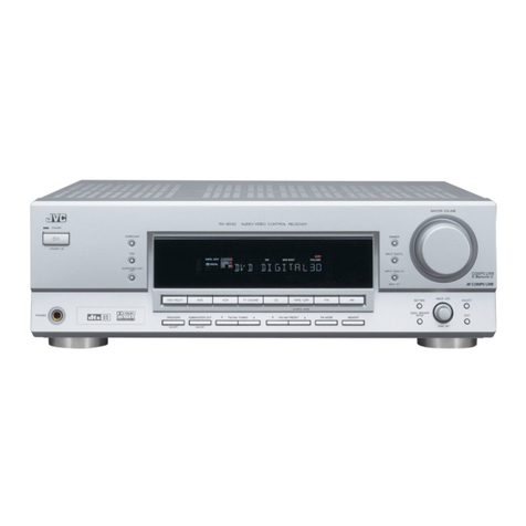
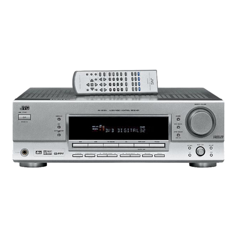
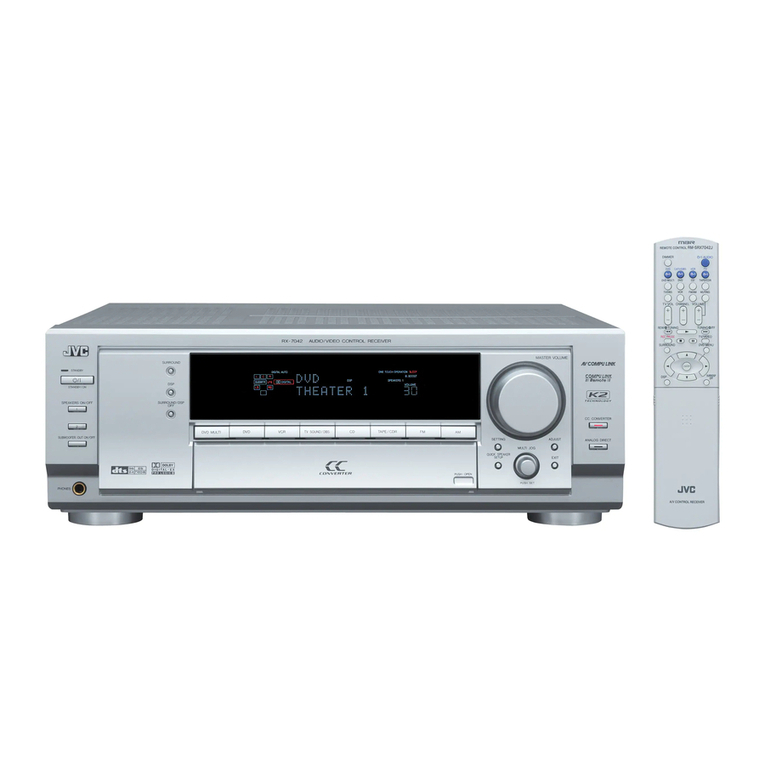
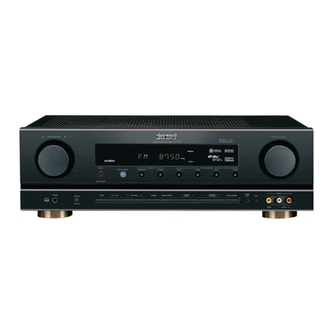
JVC RX-D201S - AV Receiver User manual

SERVICE MANUAL
COPYRIGHT © 2005 Victor Company of Japan, Limited No.MB418
2005/11
AUDIO/VIDEO CONTROL RECEIVER
MB418200511
RX-D201S,RX-D202B
Lead free solder used in the board (material : Sn-Ag-Cu, melting point : 219 Centigrade)
TABLE OF CONTENTS
1 PRECAUTIONS . . . . . . . . . . . . . . . . . . . . . . . . . . . . . . . . . . . . . . . . . . . . . . . . . . . . . . . . . . . . . . . . . . . . . . . 1-3
2 SPECIFIC SERVICE INSTRUCTIONS . . . . . . . . . . . . . . . . . . . . . . . . . . . . . . . . . . . . . . . . . . . . . . . . . . . . . . 1-6
3 DISASSEMBLY . . . . . . . . . . . . . . . . . . . . . . . . . . . . . . . . . . . . . . . . . . . . . . . . . . . . . . . . . . . . . . . . . . . . . . . 1-7
4 ADJUSTMENT . . . . . . . . . . . . . . . . . . . . . . . . . . . . . . . . . . . . . . . . . . . . . . . . . . . . . . . . . . . . . . . . . . . . . . . 1-19
5 TROUBLESHOOTING . . . . . . . . . . . . . . . . . . . . . . . . . . . . . . . . . . . . . . . . . . . . . . . . . . . . . . . . . . . . . . . . . 1-19
Area suffix
RX-D201S
Area suffix
RX-D202B
E ---------- Continental Europe
A ------------------------ Australia
B ------------------------------ U.K.
E ---------- Continental Europe
EN ----------- Northern Europe
EV ------------- Eastern Europe
UF ------------------------------ China

1-2 (No.MB418)
SPECIFICATION
* Corresponding to Linear PCM, Dolby Digital, and DTS (with sampling frequency -32 kHz, 44.1 kHz, 48 kHz).
Designs and specifications are subject to change without notice.
Amplifier
Output Power At stereo operation Front channels 100 W per channel, min. RMS, driven into 6 Ωat 1 Hz
with no more than 0.8% total harmonic distortion. (IEC-
286-3)
At surround operation Front channels 100 W per channel, min. RMS, driven into 6 Ωat 1 kHz
with no more than 0.8% total harmonic distortion.
Center channel 100 W, min. RMS, driven into 6 Ωat 1 kHz, with no more
than 0.8% total harmonic distortion.
Surround channels 100 W per channel, min. RMS, driven into 6 Ωat 1 kHz,
with no more than 0.8% total harmonic distortion.
Surround back channels 100 W per channel, min. RMS, driven into 6 Ωat 1 kHz,
with no more than 0.8% total harmonic distortion.
Audio Audio Input Sensitivity/Impedance DVR/DVD, VCR, DBS, TV:270 mV/47 kΩ
Audio Input (DIGITAL IN)* Coaxial DIGITAL IN 1(DVR/DVD):0.5 V(p-p)/75 Ω
Optical DIGITAL IN 2(DBS):-21 dBm to -15 dBm (660 nm ±30
nm)
USB USB DIGITAL
Audio Output Level DVR, VCR:270 mV
Signal-to-Noise Ratio ('66 IHF/'78 IHF) 80 dB/62 dB
Frequency Response (6 Ω) 20 Hz to 20 kHz (±1 dB)
Bass Boost +4 dB ±1 dB at 100 Hz
Equalization (at DSP operation) Center frequency 63 Hz, 250 Hz, 1 kHz, 4 kHz, 16 kHz
Control range ±8 dB
Video Video Input Sensitivity/Impedance Composite video:DVR/DVD, VCR, DBS 1 V(p-p)/75 Ω
S-video:DVR/DVD, VCR, DBS Y (luminance):1 V(p-p)/75 Ω
C (chrominance, burst):0.3 V(p-p)/75 Ω
Component:DVR/DVD, VCR (DBS) Y (luminance):1 V(p-p)/75 Ω
PB, PR:0.7 V(p-p)/75 Ω
Video Output Level/Impedance Composite video:DVR/DVD, VCR, DBS 1 V(p-p)/75 Ω
S-video:DVR, VCR, MONITOR OUT Y (luminance):1 V(p-p)/75 Ω
C (chrominance, burst):0.3 V(p-p)/75 Ω
Component:MONITOR OUT Y (luminance):1 V(p-p)/75 Ω
PB, PR:0.7 V(p-p)/75 Ω
Synchronization Negative
FM tuner (IHF)
Tuning Range 87.5 MHz to 108.0 MHz
Usable Sensitivity Monaural 17.0 dBf (1.9 µV/75 Ω)
50 dB Quieting Sensitivity Monaural 21.3 dBf (3.2 µV/75 Ω)
Stereo 41.3 dBf (31.8 µV/75 Ω)
Stereo Separation at REC OUT 35 dB at 1 kHz
AM tuner
Tuning Range 522 kHz to 1 629 kHz
General
Power Requirements AC 230 V , 50 Hz
Power Consumption 180 W (at operation)
0.9 W (in standby mode)
Dimensions (W ×H ×D) 435 mm ×91.5 mm ×360 mm
Mass 6.7 kg
(No.MB418)1-5
1.6 Caution after repairs
There are two power supply as the second power supply of the transformer.
One is a power supply for power IC(3pin), and another is a power supply for the control(8pin).
There are two power supply as the second power supply of the transformer.
One is a power supply for power IC(3pin), and another is a power supply for the control(8pin).
Please connect first of all and confirm the power supply for the control when you do the energizing examination after it completes of
the repair.
Please never do the energizing examination in a power supply of power IC alone.
Moreover, when the control system breaks down, power IC is occasionally damaged.
+B for power IC
(3pins)
+B for control section
(8pins)
For power IC(3pins)

(No.MB418)1-7
SECTION 3
DISASSEMBLY
3.1 Main body section
3.1.1 Removing the top cover
(See Figs.1 and 2)
(1) From the both sides of the main body, remove the four
screws Aattaching the top cover. (See Fig.1)
(2) From the back side of the main body, remove the six
screws Battaching the top cover. (See Fig.2)
(3) Remove the top cover in the direction of the arrow. (See
Fig.1.)
Fig.1
Fig.2
A
Top cover
B
B
Top cover
[For Australia/China]
[For Europe]
B
Top cover
B

1-8 (No.MB418)
3.1.2 Removing the front panel assembly
(See Figs.3 and 4)
• Remove the top cover.
Reference:
Remove the tie bands and wire holder bundling the wires.
(1) Disconnect the card wire from the connector CN102 on the
main amplifier board. (See Fig.3)
(2) Disconnect the wire from the connector CN351 on the main
amplifier board. (See Fig.3)
(3) Disconnect the wire from the connector CN552 on the input
board. (See Fig.3)
(4) Disconnect the wire from the connector CN661 on the vol-
ume board. (See Fig.3)
(5) Remove the three screws Cattaching the front panel as-
sembly. (See Fig.3)
(6) Remove the screw Cattaching the OSD connect 2 board.
(See Fig.3)
(7) From the bottom side of the main body, remove the four
screws Dattaching the front panel assembly. (See Fig.4)
(8) Release the joints aand remove the front panel assembly
in the direction of the arrow. (See Fig.4)
Fig.3
Fig.4
C
Front panel assembly
C
C
OSD connect 2 board
Main amplifier board
CN351
Volume board
CN552
Input board
CN661
[For Australia/China]
[For Europe]
Front panel assembly
C
C
OSD connect 2 board
Main amplifier board
CN351
Volume board
CN552
Input board
CN661
C
CN102
CN102
DFront panel assembly D
aa

(No.MB418)1-9
3.1.3 Removing the rear panel
(See Fig.5)
• Remove the top cover.
(1) From the back side of the main body, remove the strain re-
lief from the rear panel in the direction of the arrow and re-
move the power cord.
(2) Remove the twenty-four screws Eattaching the rear panel.
[For Australia/China]
(3) Remove the twenty-five screws Eattaching the rear panel.
[For Europe]
Fig.5
3.1.4 Removing the tuner
(See Fig.6)
• Remove the top cover.
(1) From the top side of the main body, disconnect the card
wire from the connector CN1 on the tuner.
(2) From the back side of the main body, remove the two
screws Fattaching the tuner to the rear panel and take out
the tuner.
3.1.5 Removing the subwoofer board
(See Fig.6)
• Remove the top cover.
(1) From the top side of the main body, disconnect the wire
from the connector CN524 on the subwoofer board.
(2) From the back side of the main body, remove the screw G
attaching the subwoofer board to the rear panel and take
out the subwoofer board.
3.1.6 Removing the compulink board
(See Fig.6) [For Australia/China]
• Remove the top cover.
(1) From the top side of the main body, disconnect the wire
from the connector CN565 on the compulink board.
(2) From the back side of the main body, remove the screw H
attaching the compulink board to the rear panel and take
out the compulink board.
Fig.6
Power cord
Strain relief Rear panel
EE
E
E
EE
Rear panel
Power cord
Strain relief
[For Australia/China]
[For Europe]
Tuner Subwoofer board
CN524
CN1
GF
Rear panel
H
Rear panel
CN565
Compulink board

1-10 (No.MB418)
3.1.7 Removing the volume board
(See Fig.7)
• Remove the top cover.
(1) From the back side of the main body, remove the three
screws Jattaching the volume board to the rear panel.
(2) Remove the screw Kattaching the volume board.
Reference:
Remove the tie bands bundling the wires.
(3) Rmove the screw Mattaching the wire holder board and
move the wire holder board with the wires in the direction
of the arrow.
(4) Disconnect the connector CN681 on the volume board in
an upward direction.
Note:
When removing the volume board, take care not to break
the claw of the connector.
(5) Take out the volume board and disconnect the wires from
the connectors (CN661, CN682, CN683) on the forward
side of the volume board.
Fig.7
3.1.8 Removing the primary board
(See Fig.8)
• Remove the top cover.
(1) From the top side of the main body, disconnect the wire
from the connector CN101 on the main amplifier board.
Reference:
Remove the tie band bundling the wire.
(2) Disconnect the power cord from the connector CN120 on
the primary board.
(3) Remove the four screws Nattaching the primary board.
Reference:
When reassembling, attach the wire holder as before.
(4) Take out the primary board from the main body and remove
the wires from the soldered sections bon the reverse side
of the primary board.
Fig.8
CN661
CN683
K
Wire holder board
CN682
M
J
Rear panel
CN681
Volume board
N
N
N
b
CN120
N
Main amplifier beard
CN101
Primary board

(No.MB418)1-11
3.1.9 Removing the power transformer
(See Fig.9)
• Remove the top cover.
Reference:
Remove the tie bands bundling the wires.
(1) Disconnect the wires from the connectors (CN106, CN111)
on the main amplifier board.
(2) Remove the soldered sections cand remove the wires.
(3) Remove the four screws Pand take out the power trans-
former from the main body.
3.1.10 Removing the trans primary board
(See Fig.9)
• Remove the top cover.
Reference:
Remove the tie band bundling the wires.
(1) Remove the wires from the soldered sections cand re-
move the wires.
(2) Remove the solders from the soldered sections dand re-
move the trans primary board.
3.1.11 Removing the trans secondary board
(See Fig.9)
• Remove the top cover and power transformer.
From the side of the power transformer, remove the solders from
the soldered sections eand remove the trans secondary board.
Fig.9
P
PP
CN106
CN111
Main amplifier board
Power transformer
e
d
c
Trans primary
board
Trans secondary
board
[For Australia/China]
[For Europe]
P
CN106
Main amplifier board
P
CN111
P
c
d
e
Trans primary
board
Trans secondary
board
Power transformer

1-12 (No.MB418)
3.1.12 Removing the DCDC control board
(See Fig.10)
• Remove the top cover.
Reference:
Remove the tie band bundling the wires.
Disconnect the connector CN151 on the DCDC control board
from the main amplifier board in an upward direction.
Note:
When removing the DCDC control board, take care not to
break the claw of the connector on the main amplifier board.
Fig.10
3.1.13 Removing the PWM modulation 1 board
(See Fig.11)
• Remove the top cover.
Reference:
Remove the tie band bundling the wires.
(1) Disconnect the wire from the connector CN413 on the
PWM modulation 2 board.
(2) Disconnect the wires from the connectors (CN311, CN312,
CN313) on the PWM modulation 1 board.
(3) Disconnect the connector CN301 on the PWM modulation
1 board from the main amplifier board in an upward direc-
tion.
Note:
When removing the PWM modulation 1 board, take care not to
break the claw of the connector on the main amplifier board.
3.1.14 Removing the PWM modulation 2 board
(See Fig.11)
• Remove the top cover.
(1) From the top side of the main body, disconnect the wires
from the connectors (CN411, CN412, CN413) on the PWM
modulation 2 board.
(2) Disconnect the connector CN401 on the PWM modulation
2 board from the main amplifier board in an upward direc-
tion.
Note:
When removing the PWM modulation 2 board, take care not to
break the claw of the connector on the main amplifier board.
Fig.11
DCDC control board Main amplifier board
CN151
CN312
CN301
CN401
CN313 CN311
CN413
CN412
CN411
PWM modulation 2 board
PWM modulation 1 board
Main amplifier board

(No.MB418)1-13
3.1.15 Removing the fan motor
(See Fig.12)
• Remove the top cover.
Reference:
Remove the tie band bundling the wires.
(1) Disconnect the wire from the connector CN103 on the main
amplifier board.
(2) Remove the two screws Q.
Reference:
When attaching the fan motor assembly, attach the wire
holder with it as before.
(3) Take out the fan motor assembly.
(4) Remove the two screws Rattaching the fan motor to the
fan bracket.
Fig.12
3.1.16 Removing the scart board
(See Fig.13) [For Europe]
• Remove the top cover.
(1) From the back side of the main body, remove the six
screws Sattaching the scart board to the rear panel.
(2) From the top side of the main body, disconnect the card
wire from the connector CN537 on the scart board and take
out the scart board from the main body.
Fig.13
3.1.17 Removing the speaker terminal 1 and speaker terminal 2 boards
(See Fig. 14)
• Remove the top cover and rear panel.
Reference:
Remove the tuner and subwoofer board as required.
(1) From the top side of the main body, disconnect the wires
from the connectors (CN261, CN461) on the speaker ter-
minal 1 board.
(2) Take out the speaker terminal 1 board from the main body.
(3) Disconnect the wires from the connectors (CN209, CN262)
on the speaker terminal 2 board.
(4) Take out the speaker terminal 2 board from the main body.
Fig.14
CN103
R
Fan motor
R
Fan bracket
Fan motor assemly
Main amplifier board
Q
Q
Scart board
CN537
S
SRear panel
CN261
CN262 CN461
CN209
Speaker terminal 2 board Speaker terminal 1 board

1-14 (No.MB418)
3.1.18 Removing the DSP connect board
(See Fig.15)
• Remove the top cover, rear panel, tuner and volume board.
Disconnect the connector CN602 on the DSP connect board
from the input board in an upward direction.
Note:
When removing the DSP connect board, take care not to break
the claw of the connector on the input board.
3.1.19 Removing the input board
(See Fig. 15)
• Remove the top cover, rear panel, tuner, volume board, scart
board and DSP connect board.
Reference:
Remove the tie bands bundling the wires.
(1) Disconnect the wire from the connector CN209 on the
speaker terminal 2 board.
(2) Disconnect the wire from the connector CN513 on the OSD
connect 1 board.
(3) Disconnect the wires from the connectors (CN530, CN531,
CN552) on the input board.
(4) Disconnect the parallel wire from the connector CN540 on
the input board.
(5) Remove the three screws Tand take out the input board
from the main body.
Fig.15
OSD connect 1 board
CN513
CN531
CN530
CN552
CN540
Input board
Speaker terminal 2 board
CN209
TT
T
CN602
DSP connect board
CN602
DSP connect board
T
CN552
CN540
CN530
CN531
T
Input board T
Speaker terminal 2 board
CN209
CN513
OSD connect 1 board
[For Australia/China]
[For Europe]

(No.MB418)1-15
3.1.20 Removing the OSD connect 1 board
(See Fig.16)
• Remove the top cover and volume board.
Reference:
Remove the tie band bundling the wires.
(1) Disconnect the wire from the connector CN524 on the sub-
woofer board.
(2) Disconnect the wire from the connector CN513 on the OSD
connect 1 board.
(3) Disconnect the connector CN522 on the OSD connect 1
board from the main amplifier board in an upward direction.
Note:
When removing the OSD connect 1 board, take care not to
break the claw of the connector on the main amplifier board.
Fig.16
3.1.21 Removing the master clock board
(See Fig.17)
• Remove the top cover, tuner, volume board, PWM modulation
1 board, PWM modulation 2 board and OSD connect 1 board.
(1) Remove the two screws Uwith a short driver and remove
the transistor hold from the joints fof the heat sink.
(2) Disconnect the wire from the connector CN201 on the main
amplifier board.
(3) Take out the master clock board from the main body.
Fig.17
CN522
CN513
OSC connect 1 board Main amplifier board
Subwoofer board
CN524
U
ff
Heat sink Transistor hold
Master clock board
Main amplifier board
CN201

1-16 (No.MB418)
3.1.22 Removing the main amplifier board
(See Figs.18 and 19)
• Remove the top cover, tuner, volume board, DCDC control
board, PWM modulation 1 board, PWM modulation 2 board,
OSD connect 1 board and master clock board.
(1) Disconnect the wire from the connector CN261 on the
speaker terminal 1 board. (See Fig.18.)
(2) Disconnect the wire from the connector CN262 on the
speaker terminal 2 board. (See Fig.18.)
Reference:
Remove the tie bands bundling the wires.
(3) Disconnect the wires from the connectors (CN101, CN103,
CN106, CN111, CN351) on the main amplifier board. (See
Fig.18.)
(4) Disconnect the card wire from the connector CN102 on the
main amplifier board. (See Fig.18.)
(5) Disconnect the wires from the connectors (CN530, CN531)
on the input board. (See Fig.19.)
(6) Disconnect the parallel wire from the connector CN540 on
the input board. (See Fig.19.)
(7) Remove the four screws Vand two screws W. (See
Fig.19.)
(8) Take out the main amplifier board with the regulator board
from the main body.
Fig.18
Fig.19
CN351
Main amplifier board
CN111
CN106
CN101
Speaker terminal 1 board
CN261
Speaker terminal 2 board
CN103 CN102
CN262
W
Regulator board
Main amplifier board
V
V
V
CN531
CN530
CN540
Input board

(No.MB418)1-17
3.1.23 Removing the regulator board
(See Fig.20)
• Remove the top cover, tuner, volume board, DCDC control
board, PWM modulation 1 board, PWM modulation 2 board,
OSD connect 1 board, master clock board and main amplifier
board.
(1) From the forward side of the main amplifier board, discon-
nect the wire from the connector CN105.
(2) Remove the two screws Xattaching the regulator board.
(3) Remove the regulator board and disconnect the parallel
wire from the connector CN104 on the main amplifier
board.
Fig.20
3.1.24 Removing the heat sink
(See Fig.21)
• Remove the top cover, tuner, volume board, DCDC control
board, PWM modulation 1 board, PWM modulation 2 board,
OSD connect 1 board, master clock board, main amplifier
board and regulator board.
(1) From the forward side of the main amplifier board, remove
the screw Yand remove the wire holder board with the
wires.
(2) Remove the five screws Zto remove the heat sink.
Fig.21
X
CN105
Regulator board
CN104
Main amplifier board
Heat sink
Z
Main amplifier board
Z
Wire holder board
Y

1-18 (No.MB418)
3.2 Front panel assembly section
• Remove the front panel assembly.
(See "3.1.2 Removing the front panel assembly".)
3.2.1 Removing the JOG board
(See Figs. 1 and 2)
(1) From the inside of the front panel assembly, remove the
four screws Aattaching the JOG board. (See Fig.1.)
(2) Take out the JOG board while lifting it from the front panel
assembly little by little.
Reference:
The master volume knob and MULTI JOG knob are re-
moved from the front side simultaneously. (See Fig.2.)
(3) From the forward side of the JOG board, disconnect the
wire from the connector CN913. (See Fig.1)
3.2.2 Removing the OSD connect 2 board
(See Fig. 1)
(1) From the inside of the front panel assembly, remove the
two screws Aattaching the OSD connect 2 board.
(2) Disconnect the wire from the connector CN914 on the FL
board.
Fig.1
Fig.2
3.2.3 Removing the FL board
(See Fig. 3)
• Remove the JOG board.
(1) Disconnect the wire from the connector CN914 on the FL
board.
(2) Remove the eight screws Aand take out the FL board.
Fig.3
CN913
A
A
A
Front panel assembly
CN914
FL board
A
OSD connect 2 board
JOG board
Front panel assembly
MULTI JOG knob Master volume knob
A
A
Front panel assembly
CN914
FL board
A
A

2-1
A/UF version
Block diagrams
CN106CN111CN101CN152
CN151
IC111 to IC113, IC115
DCDC converter
control
PWM_V,Vout_DET
M_CLOCK
AC_DET_1
VCHANGE_1
VCHANGE_2
D1101
to
D1104
Q1101
Q1102
IC101
DCDC
converter
PWM_V
Vout_DET
AC_DET_1
M_CLOCK
VCHANGE_1
VCHANGE_2
D101
to
D104
D+5V_Mi
B+5V_Mi
D109 to D112
S2
S3
S2
Q102
VPP REG.
VPP
CN102
IC151
A+5V_DSP
REG
CN130
A+5V_DSP
+12V_RY
+12V_RY
CN131
IC152
A+9V_Vi_Tu
REG
A+9V_Vi_Tu
CN103
TO
FAN
IC153
A+5V_Vi
REG
A+5V_Vi
Q157,Q158
+/-7V REG
+/-7V
Q153
+12V_FAN
REG
FAN
Q151,Q152
Q154
FAN_ON/OFF
FAN_LOW
Q101
D+5V_Mi,B+5V_Mi
REG
CN104 CN105
CN252
CN262
RY391
RY491
ST292
SURROUND
&
SURRBACK
SLout
SRout
SBLout
SBRout
CN209FW451
SURR_RY
SURRBACK_RY
CN461
CN251
CN261
RY291
RY891
ST291
FRONT
&
CENTER
Lout
Rout
Cout
FRONT_RY
CENTER_RY
Speaker terminal section
IC851
AMP
CN322
IC451
IC461
AMP
CN422
IC261
IC361
AMP
CN421
IC251
IC351
AMP
CN321
CN312CN311 CN412CN411
IC201
MODULATER
FRONT_L
FRONT_R
CENTER
SURROUND_L
SURROUND_R
SURRBACK_L
SURRBACK_R
IC801
MODULATER
IC301
MODULATER
IC401
MODULATER
CN302
CN301
CN413
CN423
PWM modulator section
FW323
CN313
FL,FR
A.NFB_FL
D.NFB_FL
A.NFB_FR
D.NFB_FR
C
A.NFB_C
D.NFB_C
M_CLOCK
+/-7V
+/-7V
+/-7V
CN402
CN401
SL,SR
A.NFB_SL
D.NFB_SL
A.NFB_SR
D.NFB_SR
SBL,SBR
A.NFB_SBL
D.NFB_SBL
A.NFB_SBR
D.NFB_SBR
CN202
IC211 to IC214
Master clock GEN.
Q444,Q445
-B+12V REG
Master clock section
CN201
M_CLOCK
FREQ_CTRL
-B, -B+12V
FL,FR,C
SL,SR
SBL,SBR
A.NFB_SBL,D.NFB_SBL
A.NFB_SBR,D.NFB_SBR
A.NFB_FL,D.NFB_FL
A.NFB_FR,D.NFB_FR
A.NFB_C
D.NFB_C
A.NFB_SL,D.NFB_SL
A.NFB_SR,D.NFB_SR
J6501
TV
DBS
J6502
VCR
IN/OUT
J6503
DVR OUT
DVR/DVD IN
IC502
6CH
SW
TV_L/R
DBS_L/R
VCRREC_L/R
VCR_L/R
DVRREC_L/R
DVR_L/R L,R
CN503
BD DA
BD CL
FW501
L,R
J6511
DBS
VCR OUT
J6512
VCR IN
DVR OUT
J6513
DVR/DVD IN
MONITOR
IC522
SY SEL.
IC524
IC525
SC SEL.
IC527
CV SEL.
Y
C
CV
VIDEO1
VIDEO4
IC501
CPU
Y OUT
C OUT
CV OUT
CN505
TO
TUNER
TU_L/R
TU_DATAIN
TU_DATAOUT
TU_CLK
TU_CE
CN531
DSP_COMMAND
DSP_STATUS
DSP_READY
DSP_CLOCK
DSP_RESET
CN502
CN602
CN672
DA,CL
S_MUTE
SBWR_MUTE
CN530
D+5V,B+5V
+/-7V,+9V
A+5V(DSP)
D+5V(DSP)
+5V(VIDEO)
+12V(RELAY)
BCHANGE1
BCHANGE2
FAN_ON/OFF
FAN_L
POWER_ON
Q524
HP_RELAY
HP_RY
J505
AV
COMPULINK
CN565
CN555
AVCLINK
M_COMMAND,M_STATUS
M_CLK,M_RESET,M_BUSY
M_CS
FW240
CN540
PROTECT
FREQ_CTRL
CN509
FR_RELAY
C_RELAY
SURR_RELAY
SBK_RELAY
CN222
M_CLOCK
FREQ_CTRL
PROTECT
J4503
VCR IN
DVR/DVD IN
MONITOR
IC531
PB SEL.
PB OUT
PB
IC530
Y SEL.
Y OUT
Y
IC532
PR SEL.
PR OUT
PR
VIDEO1
VIDEO11
Audio/Video signal input and
system control section
Regulator, DC-DC converter and digital power amplifier section
CN513
IC503
6CH
VOLUME
L,R
IC508
AUDIO SOUND
PROCESSOR
MUTE
DSP_L/R
DSP_SL/SR
DSP_C
DSP_SW
S_MUTE
IC504
AMP
CN522
CN523
SUBWFR
CN524
J504
DA,CL
DA,CL
CN521
CN681CN682
SUBWOOFER
OUT
CN683
IC667
8CH
CODEC
DSP_IN_L
DSP_IN_R
IC671
CPU
DSPSTATUS
DSPREADY
DSPCLK
DSPRESET
DSPCOMMAND
MOSI
MISO
SS,HREQ
DSP_RST
IC673
INV
SCK
MICK
IC661
DSP
IC601
IC602
AMP.
LIN+/-
RIN+/-
IC611 to IC613
IC615,IC621,IC622
IC632 to IC634
IC651,IC652
AMP.
C_LRCK
S_LRCK
C_BCK
S_BCK
D/A0 to D/A3
DATA,XTAL
A1+/- to A4+/-
B1+/- to B4+/-
Volume section
DSP and digital signal
input terminal section
IC901
CPU
&
FL
DRV.
DI901
FL
DISPLAY
SEG1 to 35
GRID1 to 15
CN913
CN903
JS901
JS902
VOL1,VOL2
JOG1,JOG2
J901
HEADPHONE
CN904
CN914
J903
USB
TERMINAL
IC903
D/A
CN961
D+/-,VBUS USB_IN
CN905
HP_L
HP_R
CN661
RX4
J681 UN682
RX1
RX0
DIGITAL
IN1
DIGITAL
IN2
CN351
CN902
F1,F1
-VPP
D+5V
CN952
CN552
AV COMPULINK
Q910
AVC_IN/OUT
D917 to D922
FM_LED,USB_LED
TV_LED,DBS_LED
DVD_LED,VCR_LED
S901 to S906
KEY_IN1
KEY_IN2
KEY_IN3
D907
STANDBY
LED
STANDBY_LED
IC902
IR DET.
REMOCON
Use control keys, system
control and FL display section
MUTE
T_MUTE
DSP_SBL/SBR
HEADPHONE_DET
AMP_-B
AMP_-B+12V
FREQ_CTRL
PROTECT
Lout_HP
Rout_HP
Q281 to Q286
PROTECTOR
PROTECT
Lout_HP
Rout_HP
Lout_HP
Rout_HP
RY300
HP_RY
D+5V_Mi
D+5V_Mi
D+5V_DSP
B+5V_Mi
POWER_ON POWER_ON
POWER_ON
RY+9V
+12V
-B+12V
D+5V_DSP
CDIN
CDOUT
CCLK,D_CS
D_RST
GPIO1,GPIO2
GPIO3,GPIO4
CN114 CN115
Q174
DCDC_+12
REG
Q175
DCDC_-B+12
REG
Q171
D+5V_DSP
REG
Q173
PRI_RY+9V
REG
Main
plug
CN120
T102
Trans.
FW121
RY101
Q1001
POWER_ON
Primary section
Power
trans.
CN206CN211
S1
S2
S3
AC
RY+9V
MUTE
SBWR_MUTE
+B
-B

2-2
Main
plug
CN120
T102
Trans.
FW121
RY101
Q1001
POWER_ON
Primary section
Power
trans.
CN206CN211
S1
S2
S3
AC
CN106CN111CN101CN152
CN151
IC111 to IC113, IC115
DCDC converter
control
PWM_V,Vout_DET
M_CLOCK,AC_DET_1
VCHANGE_1
VCHANGE_2
D1101
to
D1104
Q1101
Q1102
IC101
DCDC
converter
PWM_V
Vout_DET
AC_DET_1
M_CLOCK
VCHANGE_1
VCHANGE_2
D101
to
D104
D+5V_Mi
B+5V_Mi
D109 to D112 S2
S3
S2
Q102
VPP REG.
VPP
CN102
IC151
A+5V_DSP
REG
CN130
A+5V_DSP
+12V_RY
+12V_RY
CN131
IC152
A+9V_Vi_Tu
REG
A+9V_Vi_Tu
CN103
TO
FAN
IC153
A+5V_Vi
REG
A+5V_Vi
Q157,Q158
+/-7V REG
+/-7V
Q153
+12V_FAN
REG
FAN
Q151,Q152
Q154
FAN_ON/OFF
FAN_LOW
Q101
D+5V_Mi,B+5V_Mi
REG
CN104 CN105
CN114 CN115
Q174
DCDC_+12
REG
Q175
DCDC_-B+12
REG
Q171
D+5V_DSP
REG
CN252
CN262
RY391
RY491
ST292
SURROUND
&
SURRBACK
SLout
SRout
SBLout
SBRout
CN209FW451
SURR_RY
SURRBACK_RY
CN461
CN251
CN261
RY291
RY891
ST291
FRONT
&
CENTER
Lout
Rout
Cout
FRONT_RY
CENTER_RY
Speaker terminal section
IC851
AMP
CN322
IC451
IC461
AMP
CN422
IC261
IC361
AMP
CN421
IC251
IC351
AMP
CN321
CN312CN311 CN412CN411
IC201
MODULATOR
FRONT_L
FRONT_R
CENTER
SURROUND_L
SURROUND_R
SURRBACK_L
SURRBACK_R
IC801
MODULATOR
IC301
MODULATOR
IC401
MODULATOR
CN302
CN301
CN413
CN423
PWM modulator section
FW323
CN313
FL,FR
A.NFB_FL
D.NFB_FL
A.NFB_FR
D.NFB_FR
C
A.NFB_C
D.NFB_C
M_CLOCK
+/-7V
+/-7V
+/-7V
CN402
CN401
SL,SR
A.NFB_SL
D.NFB_SL
A.NFB_SR
D.NFB_SR
SBL,SBR
A.NFB_SBL
D.NFB_SBL
A.NFB_SBR
D.NFB_SBR
CN202
IC211 to IC214
Master clock GEN.
Q444,Q445
-B+12V REG
Master clock section
CN201
M_CLOCK
FREQ_CTRL
-B, -B+12V
FL,FR,C
SL,SR
SBL,SBR
A.NFB_SBL,D.NFB_SBL
A.NFB_SBR,D.NFB_SBR
A.NFB_FL,D.NFB_FL
A.NFB_FR,D.NFB_FR
A.NFB_C
D.NFB_C
A.NFB_SL,D.NFB_SL
A.NFB_SR,D.NFB_SR
IC502
6CH
SW
L,R
CN503
BD DA
BD CL
FW501
IC501
CPU
CN505
TU_L/R
TU_DATAIN
TU_DATAOUT
TU_CLK,TU_CE
T_MUTE
CN531
DSP_COMMAND
DSP_STATUS
DSP_READY
DSP_CLOCK
DSP_RESET
CN502
DA,CL,S_MUTE
SBWR_MUTE
CN530
D+5V,B+5V,+/-7V,+9V
A+5V(DSP),D+5V(DSP)
+5V(VIDEO),+12V(RELAY)
BCHANGE1
BCHANGE2
FAN_ON/OFF
FAN_L
POWER_ON
Q524
HP_RELAY
HP_RY
M_COMMAND,M_STATUS
M_CLK,M_RESET,M_BUSY
M_CS
FW240
CN540
PROTECT
FREQ_CTRL
CN509
FR_RELAY
C_RELAY
SURR_RELAY
SBK_RELAY
CN222
M_CLOCK
FREQ_CTRL
PROTECT
J4503
VIDEO IN
DVR/DVD IN
MONITOR
IC531
PB SEL.
PB OUT
PB
IC530
Y SEL.
Y OUT
Y
IC532
PR SEL.
PR OUT
PR
VIDEO1
Component and scart TV section Regulator, DC-DC converter and digital power amplifier section
CN513
IC503
6CH
VOLUME
L,R
IC508
AUDIO SOUND
PROCESSOR
MUTE
DSP_L/R
DSP_SL/SR
DSP_C
DSP_SW
S_MUTE
IC504
AMP
CN522
CN523
SUBWFR
CN524
J504
DA,CL
DA
CL
CN521
CN681CN682
SUBWOOFER
OUT
CN683
IC667
8CH
CODEC
DSP_IN_L
DSP_IN_R
IC671
CPU
DSPSTATUS
DSPREADY
DSPCLK
DSPRESET
DSPCOMMAND
MOSI
MISO
SS,HREQ
DSP_RST
IC673
INV
SCK
MICK
IC661
DSP
IC601
IC602
AMP.
LIN+/-
RIN+/-
IC611 to IC613
IC615,IC621,IC622
IC632 to IC634
IC651,IC652
AMP.
C_LRCK
S_LRCK
C_BCK
S_BCK
D/A0 to D/A3
DATA,XTAL
A1+/- to A4+/-
B1+/- to B4+/-
Volume section
DSP and digital signal
input terminal section
IC901
CPU
&
FL
DRV.
DI901
FL
DISPLAY
SEG1 to 35
GRID1 to 15
CN913
CN903
JS901
JS902
VOL1,VOL2
JOG1,JOG2
J901
HEADPHONE
CN904
CN914
J903
USB
TERMINAL
IC903
D/A
CN961
D+/-,VBUS USB_IN
CN905
HP_L
HP_R
CN661
RX4
J681 UN682
RX1
RX0
DIGITAL
IN1
DIGITAL
IN2
CN351
CN902
F1,F1
-VPP
D+5V
CN952
CN552
D917 to D922
FM_LED,USB_LED
TV_LED,DBS_LED
DVD_LED,VCR_LED
S901 to S906
KEY_IN1
KEY_IN2
KEY_IN3
D907
STANDBY
LED
STANDBY_LED
IC902
IR DET.
REMOCON
User control keys, system
control and FL display section
MUTE
T_MUTE
DSP_SBL/SBR
HEADPHONE_DET
AMP_-B
AMP_-B+12V
FREQ_CTRL
PROTECT
Lout_HP
Rout_HP
Q281 to Q286
PROTECTOR
PROTECT
Lout_HP
Rout_HP
Lout_HP
Rout_HP
RY300
HP_RY
D+5V_Mi
D+5V_Mi
D+5V_DSP
B+5V_Mi
POWER_ON POWER_ON
POWER_ON
+12V
-B+12V
D+5V_DSP
CDIN
CDOUT
CCLK,D_CS
D_RST
GPIO1,GPIO2
GPIO3,GPIO4
Audio/Video signal input and
system control section
J9511
TV
CN537
CN527
TV_VOUT
TV_VY
TV_L/R
TV_G,TV_B
TV_R/C
TV_SLOW_OUT
J6503
VIDEO
DVR/DVD
VID_L/R
DVR_L/R
J8511
VCR VCR_B IC571
AMP
& SEL
IC573
BUFF
IC572
AMP
& SEL
J8512
DVR/DVD
VCR_R/C
VCR_G
DVD_B
DVD_G
IC576
SEL
V/SY IN
VCR_VY IC577
AMP
& SEL
IC574
SEL
IC575
SEL
R/SC
B
G
V/SY OUT
J8513
VIDEO
C
DVD_R/C
DVD_VY
IC581
SEL
CV
Y
Q8524
Q8525
SLOW_L
SLOW_M
VCROUT_L/R
DVROUT_L/R
VCROUT_L/R
DVROUT_L/R
VCR_L/R
DVR_L/R
TU_L/R
VIDEO2
VIDEO2
VIDEO1
VIDEO2 VIDEO4
VIDEO1
VIDEO2
VIDEO1
VID_S/C
TV_L/R
TO
TUNER
B,G,R/SC
V/SY IN
V/SY OUT
SLOW
L,R
IC505
RDS
RDSDA
RDSCL
IC507
EEPROM
RC_SDA
RC_SCL
RC_WP
M_COMMAND
M_STATUS
M_CLOCK
M_RESET
M_BUSY
M_CS
CN602
CN672
+B
-B
SLOW
MUTE
SBWR_MUTE
B/E/EN/EV version

2-3
SHEET 1
Parts are safety assurance parts.
When replacing those parts make
sure to use the specified one.
FC103
QNG0020-001Z
PW151
FC104
QNG0020-001Z
!
!
D1001
1SS133-T2
Q1001
KRC105S-X
PW104
C1001
4700p
!
PW151
PW152
FC113
QNG0020-001Z
!
C1002
0.22
!
!
PW155
R1002
3.3M !
PW154
CN120
QGA7901C1-02
1
2
FC103
QNG0020-001Z
PW155
PW104
C1001
4700p
!
FW121
1
2
3
4
PW153
FC114
QNG0020-001Z
EP151
QNZ0136-001Z
123
D1001
1SS133-T2
CN206
1
2
3
4
5
6
7
8
CN120
QGA7901C1-02
1
2
Q1001
KRC105S-X
CN206
1
2
3
4
5
6
7
8
PW157
CN211
QGA3901F2-03
1
2
3
EP151
QNZ0136-001Z
123
PW156
FC113
QNG0020-001Z
!
FW121
1
2
3
4
PW103
C1002
0.22
!
QQT0281-006
T102
!
9
54
1
FC114
QNG0020-001Z
RY101
!
QSK0142-001
21
43
R1002
3.3M !
PW153
RY101
!
QSK0142-001
21
43
PW157
PW103
PW154
QQT0281-006
T102
!
9
54
1
FC104
QNG0020-001Z
!
CN211
QGA3901F2-03
1
2
3
PW152
PW156
C121
0.1
PW12
C121
0.1
PW12
C1003
1000p
C1004
1000p C1003
1000p
C1004
1000p
COM
17V
!
S2
LIVE/
RY+9V
0V
COM
127V
NEUTRAL/
COM
S2
S1
0V
LVA10579-12
TH.FUSE
LVA10579-13
127V
S2
17V
S3
RY+9V
COM
S1
S3
BRN
TH.FUSE
S3
LIVE/
S1
BLU
127V
!
POWER_ON
BLU
AC
0V
POWER_ON
BRN
S1
AC
110V
AC
127V
LVA10579-5 LVA10579-5
NEUTRAL/
0V
S2
LVA10579-13
S3
LVA10579-12
AC
110V
F103
F104
F103
F104
TO CN111 OF LVA10578-1
(SHEET 3)(SHEET 3)
TO CN106 OF LVA10578-1
(SHEET 3)(SHEET 3)
TO CN106 OF LVA10578-1 TO CN111 OF LVA10578-1
to CN101 of LVA10578-1
(SHEET 3)
(SHEET 3)
of LVA10578-1to CN101
MAINS
PLUG
UP/UF
MAINS
A
PLUG
Standard schematic diagrams
Primary section (For A/UF version)

2-4
SHEET 2
Parts are safety assurance parts.
When replacing those parts make
sure to use the specified one.
PW157
PW156
PW155
PW154
PW153
PW152
PW151
CN211
QGA3901F2-03
1
2
3
CN206
1
2
3
4
5
6
7
8
PW151
CN211
QGA3901F2-03
1
2
3
CN206
1
2
3
4
5
6
7
8
PW157
PW156
PW155
PW154
PW153
PW152
PW113
PW57
PW56
PW55
PW54
VS101
QSW0812-001
!
8
1
7
4
6
3
5
2
PW53
PW52
FC115
QNG0020-001Z
FC105
QNG0020-001Z
PW151
CN211
QGA3901F2-03
1
2
3
CN206
1
2
3
4
5
6
7
8
PW157
PW156
PW155
PW154
PW153
PW152
C1001
4700p
!
B142
QUY158-150Y
Q1001
KRC105S-X
FW121
1
2
3
4QQT0478-001
T102
!
9
54
1
PW103
RY101
!
QSK0128-001
21
43
FC103
QNG0020-001Z
D1001
1SS133-T2
FC113
QNG0020-001Z
!
CN120
QGA7901C1-02
1
2
EP151
QNZ0136-001Z
123
C1002
0.22
!
R1002
3.3M !
R1001
3.3M
PW104
C1001
4700p
!
Q1001
KRC105S-X
FW121
1
2
3
4QQT0478-002
T102
!
!
9
54
1
PW103
RY101
!
QSK0128-001
21
43
FC103
QNG0020-001Z
D1001
1SS133-T2
FC113
QNG0020-001Z
!
CN120
QGA7901C1-02
1
2
FC114
QNG0020-001Z
EP151
QNZ0136-001Z
123
C1002
0.22
!
R1002
3.3M !
FC104
QNG0020-001Z
!
PW104
C1001
4700p
!
Q1001
KRC105S-X
FW121
1
2
3
4QQT0281-006
T102
!
9
54
1
PW103
RY101
!
QSK0142-001
21
43
FC103
QNG0020-001Z
D1001
1SS133-T2
FC113
QNG0020-001Z
!
CN120
QGA7901C1-02
1
2
FC114
QNG0020-001Z
EP151
QNZ0136-001Z
123
C1002
0.22
!
R1002
3.3M !
FC104
QNG0020-001Z
!
PW104
8
1
7
4
6
3
5
2
8
1
7
4
6
3
5
2
8
1
7
4
6
3
5
2
8
1
7
4
6
3
5
2
C121
0.1
PW12
C121
0.1
PW12
C1003
1000p
C1004
1000p
C1003
1000p
C1004
1000p
TH.FUSE
S2
COM
S2
S3
S3
S1
COM
S1
LVA10579-12
LVA10579-13
S2
LVA10579-13
TH.FUSE
LVA10579-12
S1
S3
COM
COM
S2
S3
S1
LVA10579-6
127V
0V
110V
127V
0V
17V
S2
LVA10579-13
TH.FUSE
LVA10579-12
S1
S3
COM
COM
S2
S3
S1
POWER_ON
RY+9V
BRN
!
AC NEUTRAL/
LIVE/
BLU
AC
of LVA10578-1to CN101
LVA10579-5
POWER_ON
RY+9V
BRN
!
AC NEUTRAL/
LIVE/
BLU
AC
LVA10579-5
POWER_ON
RY+9V
BRN
!
AC NEUTRAL/
LIVE/
BLU
AC
LVA10579-5
220V 230-240V127V110V
VOLTAGE SELECTOR LOCATION
SOURCE FM(NO SIGNAL)
VOLTAGE MEASUREMENT CONDITION
POWER ON
VOLUME 0
SURROUND OFF
VERSION CODES
J ;U.S.A.
C ;CANADA
B ;U.K.
E ;CONTINENTAL EUROPE
EN:NORDIC COUNTRIES
EV;EAST EUROPEAN COUNTRIES
US;SINGAPORE
UJ;U.S. ARMY
A ;AUSTRARIA
UP;KOREA
UF;CHINA
UN;INDONESIA
UT;TAIWAN
F103 F103
F104
F103
F104
F103
F104
J/C B/E/EN/EV US/UJ/UN/UT A UP/UF
QMF51U1-6R3-J8
-
QMF51W2-2R5-J8
QMF5AE2-R10-J1
QMF51W2-5R0-J8
QMF5AE2-R10-J1
QMF51W2-5R0-J8 QMF51W2-5R0-J8
QMF5AE2-R10-J1 QMF5AE2-R10-J1
TO CN111 OF LVA10478-1TO CN106 OF LVA10478-1
to CN101 of LVA10578-1
TO CN111 OF LVA10578-1
(SHEET 3)(SHEET 3)
TO CN106 OF LVA10578-1
to CN101 of LVA10578-1
(SHEET 3)
J/C US/UJ/UN/UT
B/E/EN/EV
PLUG
MAINS
PLUG
MAINS
PLUG
MAINS
Primary section (For B/E/EN/EV version)

2-5
SHEET 3
Parts are safety assurance parts.
When replacing those parts make
sure to use the specified one.
+
-
+
-
+
-
IC112
NJM2403M-X 2
3
1
8
4
R1156
120k
C1174
100/16
R1151
3.6k
C1154
100p
R1160
1k
R1172
3.3k
D1152
1SS133-T2IC113
SN74HC00ANS-X
891011121314
7654321
C1157
0.1
R1163
330
R1159
10k
C1155
1
R1152
6.8k
C1182
100/16
R1162
1k
Q1173
KTA1504/YG/-X
C1152
1
C1153
1
R1157
10k
IC111
NJM2125F-X
3
1
4
5
2
R1166
470
D1174
1SS133-T2
R1165
3.3k
Q1171
KTC3875/YG/-X
C1181
0.01
R1174
18k
R1164
47k
R1175
2.2k
R1161
1M
C1173
0.01
C1151
47/16
D1153
1SS133-T2
R1176
47k
C1156
100p
D1173
1SS133-T2
Q1172
KRC102S-X
D1172
1SS133-T2
R1158
820
R1154
3.3k
IC121
KIA7805API
1
2
3
R1153
2.2k
D1151
1SS133-T2
R1173
10k
IC112
NJM2403M-X
6
5
7
R1155
22k
Q1151
KRC102S-X
Q1152
KRC102S-X
C1172
1000p
IC115
SN74HC74ANS-X
891011121314
7654321
C1158
0.1
D1154
UDZS2.7B-X
R1170
1k
R1169
3.3k
Q1174
KTC3875/YG/-X
R1178
100
Q1103
KTA1268/GL/-T
R1114
820
D1155
1SS133-T2
R1180
13k
R1179
3.3k
C1159
820p
CN151
QGB2510K1-11
1
2
3
4
5
6
7
8
9
10
11
Q1176
KRA102S-X
Q1175
KTC3875/YG/-X
FEEDBACK
VCC
GND
+12V
Vout_DET
VCHANGE_1
VCHANGE_2
M_CLOCK
PGND
PWM_V
(1/2)
(2/2)
1CLR
1D
1CLK
1PRE
1Q
1Q
GND 2Q
2Q
2PRE
2CLK
2D
2CLR
VCC
DCDC Converter_Control
LVA10579-11
AC_DET_2
AC_DET_1
DRIVER_SD
C164
2200p
D158
MTZJ6.2C-T2
C165
100/16
B2553
C166
470/16
R165
0.22
UNF
(1W)
!
R166
2.2k
UNF
(1/4W)
!
Q171
2SD2394/EF/
!
B2554
Q173
2SD2394/EF/
!
C172
4700p
C174
10/50
C173
1/50
Q174
2SD2394/EF/
!
D171
MTZJ13B-T2
C176
10/50
C175
1/50
Q175
2SD2394/EF/
!
D172
MTZJ13B-T2
R173
4.7
UNF
!
R174
10k
UNF
!
R175
4.7
UNF
!
R176
10k
UNF
!
CN115
1
2
3
4
5
CN114
QGA2001F1-07
1
2
3
4
5
6
7
D+5V_DSP
PRI_RY+9V
+12V
+B
PGND
-B+12V
-B
(1/2W)
(1/2W)
(1/2W)
(1/2W)
DCDC_+12
LVA10578-4
to CN104
of LVA10578-1
to CN104
of LVA10578-1
*
*
C1122
0.33
D1103
30PRA20-FC
!
D1104
30PRA20-FC
!
D1105
C1103
L1102
QQL78AK-220
33
!
R1103
33 1/4W !
IC101
IRS2011S-X
8765
1234
Q1102
2SK3599-01MR
!
D
G
S
C1104
C1118
2200/50
R1111
1k
D1106
C1117
2200/50
R1112
1k
L1101
QQL78AK-220
33
!
R1105
10
C1113
0.0033
R1108
10
D1102
30PRA20-FC
!
D1171
1SS133-T2
C1171
4.7/50
C1101
0.22/100
C1120
0.1/100
C1109
0.0033
C1116
0.1/100
R1106
10
D1108
FMB-G19L
!
C1105 6800/71
C1106
6800/71
D1107
FMB-G19L
!
R1113
39k
R1115 820
C1102
0.22/100
D1109
1SS133-T2
C1119
0.1/100
C1111
0.0033
C1107
0.0033
C1123
1
R1107
10
C1115
0.1/100
Q1101
2SK3599-01MR
!
D
G
S
R1104
33 1/4W
!
D1101
30PRA20-FC
!
D111
10DDA20-FD
!
D110
10DDA20-FD
!
D109
10DDA20-FD !
D112
10DDA20-FD
!
C152
3300/25
TH101
4.7
!
C110
220/50
D113
1A3G-T1
!
D114
1A3G-T1
!
D115
1A3G-T1
!
C112
22/50
Q102
KTA1046/Y/
!
D116
MTZJ36C-T2
C113
22/50
R109
22k
Q103
KTC3200/GL/-T
D117
MTZJ8.2C-T2
C114
1/50
R110
100k
IC151
KIA7805API
!
1
2
3
IC153
KIA7805API
!
1
2
3
IC152
KIA7809API
!
1
2
3
C153
0.01
C158
0.01
C155
0.01
C154
100/16
C159
100/16
C156
100/25
Q157
2SD2394/EF/ !
C160
100/16
D156
MTZJ8.2C-T2
D157
MTZJ8.2C-T2
C162
100/16
D103
1A3G-T1
!
D104
1A3G-T1
!
D101
1A3G-T1
!
D102
1A3G-T1
!
C101
0.0047/100
C102
C103
4700p
Q101
KTD863/Y/-T
!
D106
MTZJ6.2B-T2
C104
470/16
Q158
KTA1046/Y/
!
CN101
QGA2001C1-04
1
2
3
4
D107
1A3G-T1
D108
1A3G-T1
CN102
QGF1205C1-05
1
2
3
4
5
Q153
2SD2394/EF/
!
Q151
KRA102S-X
Q152
KRC102S-X
D152
1SS133-T2
C157
10/50
D153
MTZJ13B-T2
D154
MTZJ9.1C-T2
Q154
KRC102S-X
D161 1A3G-T1
D162
1A3G-T1
R154
10k
R155
11k
R159
2k
R160
47k
C161
470/16
C163
470/16
CN103
QGA2501C1-02
1
2
R1101
100k
R1102 100k
B2017
D105
MTZJ12C-T2
C111
100/63
R101
15k
UNF
R102
3.3k
UNF
R103
6.8
UNF
!
R104
10
UNF
R106
820
UNF
R107
UNF
(1/4W)
!
R108
3.3k
UNF
!
R157
560
UNF
!
R158
4.7
UNF
!
R162
2.2k
UNF
!
R164
2.2k
UNF
!
R1109
2.2k
UNF
2W
R1110
2.2k
UNF
2W
R1171
3.3k
UNF
CN131
1
2
3
4
5
6
7
8
9
R151
10 UNF
!
R153
4.7
UNF
!
CN105
QGA2001C1-05
1
2
3
4
5
R272
NI
TH272
QAD0146-103
!
!
!
AMP_+B
PGND
AMP_-B
HP_RY
TH_COM
TH2
+12V_RY
R105
10
UNF
C106
0.1/100
MY
C107
0.1/100
MY
C105
0.1/100
MY
C109
0.047
MY
C108
0.047
MY
R152 4.7 UNF
!
R161
4.7
UNF
!
R163
10
UNF
!
R156
10 UNF
!
BLK_DCCTRL
C1108
0.0033
C1110
0.0033
C1112
0.0033
C1114
0.0033
FC101
QNG0020-001Z
!
FC111
QNG0020-001Z
FC112
QNG0020-001Z
FC102
QNG0020-001Z
!
R1116
4.7
1/4W
CN104
7
6
5
4
3
2
1
CN130
1
2
3
4
5
6
7
8
9
10
11
CN106
QGA3901C1-08
1
2
3
4
5
6
7
8
CN111
QGA3901C1-03
1
2
3
BLK_REG
R183
2k
R184
47k
Q161
KRC111S-X
Q163
KRC111S-X
Q162
KRC111S-X
R181
100
R182
2.2k
C1126
NI
R1117
4.7
1/4W
!
D1110
1SS133-T2
DRIVER_SD
CN152
QGB2510J1-11
1
2
3
4
5
6
7
8
9
10
11
Q1104
KTA1268/GL/-T
D1111
1SS133-T2
R1118
47k
FW323
1
2
3
4
EP102
QNZ0136-001Z
EP101
QNZ0136-001Z
C151
4700/25
C1124
0.1/250
C1125
0.1/250
C1164
C1163
C1145 0.22/100
C1144 0.22/100
C1162
C1161
C1143 0.22/100
C1142 0.22/100
C1147
0.1/250
C1149
C1150
C1146
0.1/250
C1135
0.1/250
C1136
0.1/250
C1137
0.1/250
C1138
0.1/250
C1148
C1134 0.22/100
C1133 0.22/100
C1132 0.22/100
C1131 0.22/100
HIN
VCCLO
COM
LIN
VB
HO
VS
D+5V_Mi
DGND
FL1
VPP
FL2
+7V
-7V
AGND
A+5V_DSP
A+5V_Vi
A+9V_Vi_Tu
+12V_RY
D+5V_Mi
B+5V_Mi
D+5V_DSP
DGND
FAN_ON/OFF
FAN_LOW
POWER_ON
REG_DET
D+5V_HDMI
AC
AC
RY+9V
POWER_ON
S2
COM
S2
S3
S3
FAN
FANGND
+12V
FEEDBACK
AC_DET_1
Vout_DET
VCHANGE_2
M_CLOCK
PGND
PWM_V
A+5V_DSP
A+9V_Vi_Tu
+12V_FAN
A+5V_Vi
+7V
-7V
(1/4W)
(1W)
(1/4W)
(1/4W)
(1/4W)
(1/4W)
(1/2W)
(1/4W)
(1/2W)
(1/4W)
(1/4W)
(1/2W)
(1/4W)
(1/4W)
(1/4W)
(1/4W)
(1W)(1W)(1W) (1W)
(1/4W)
(With H.Sink)
(With H.Sink)
(With H.Sink)
(With H.Sink)
(With H.Sink)
(With H.Sink)
(With H.Sink)
(With H.Sink)
(With H.Sink)
(With H.Sink)
DCDC Converter
VCHANGE_1
VCHANGE_2
HP_RY
(1/4W)
VCHANGE_1
AC_DET_2
AC_DET_2
M_CLOCK
+7V
-7V
AGND
N.I.
N.I.
DRIVER_SD
to CN313
of LVA10578-2
*
**
*
*
*
*
*MARK LIST
C102
R101
R102
R104
R105
D105
B2017
Q173
C172
US,UP,A,UF,
UN,UT,UJ
J,C,B,E,EN,EV
220/63 1000/25
USE NONE
USE NONE
USE NONE
USENONE
USE NONE
USENONE
USE
USE
NONE
NONE
LVA10578-1
F102
F101
FROM CN206 OF LVA10579-13
(SHEET 1) or (SHEET 2) (SHEET 1) or (SHEET 2)
FROM FW121 OF LVA10579-5
FROM CN211 OF LVA10579-13
(SHEET 1) or (SHEET 2)
(SHEET 4)
TO CN531 OF LVA10577-1
TO CN531 OF LVA10584-1
TO CN530 OF LVA10577-1
TO CN530 OF LVA10584-1
(SHEET 6) or (SHEET 8)
TO CN902 OF LVA10579-1
(SHEET 12)
(SHEET 5)
*
R107
J,C B,E,EN,EV US,UP,A,UF,
UN,UT,UJ
5.6 5.6 6.2
N.I.
N.I.
*
**
*
N.I.
N.I.
*
N.I.
N.I.
*
*
N.I.
*
*
*
*
*
J,C B,E,EN,EV,US,
UP,A,UF,UN,UT,UJ
N.I.
N.I.
C1142
C1143
C1144
C1145
C1135
C1138
C1146
C1147
C1131
C1132
C1133
C1134
NONE USE
NONE
NONE
NONE
NONE
NONE
NONE
NONE
NONE
NONE
NONE
NONE
USE
USE
USE
USE
USE
USE
USE
USE
USE
USE
USE
*MARK LIST
DCDC_-B+12
!
TO
FAN
(SHEET 5)
(SHEET 4)
(SHEET 5)
(SHEET 5)
Regulator and DC-DC converter section (Common)
Other manuals for RX-D201S - AV Receiver
4
This manual suits for next models
1
Table of contents
Other JVC Receiver manuals

JVC
JVC RX-6020VBK User manual

JVC
JVC KD-X172 User manual

JVC
JVC RX-DP15B - AV Receiver User manual

JVC
JVC EXAD KW-AVX708 User manual

JVC
JVC KS-RT313 User manual

JVC
JVC LVT1507-012A User manual

JVC
JVC RX-D205S - Home Theater Receiver User manual

JVC
JVC KD-R775S User manual

JVC
JVC RX-F10S User manual

JVC
JVC KS-FX711 Guide