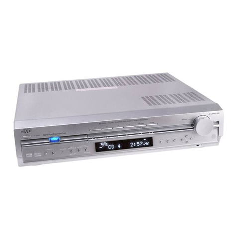
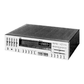
JVC R-S77 User manual

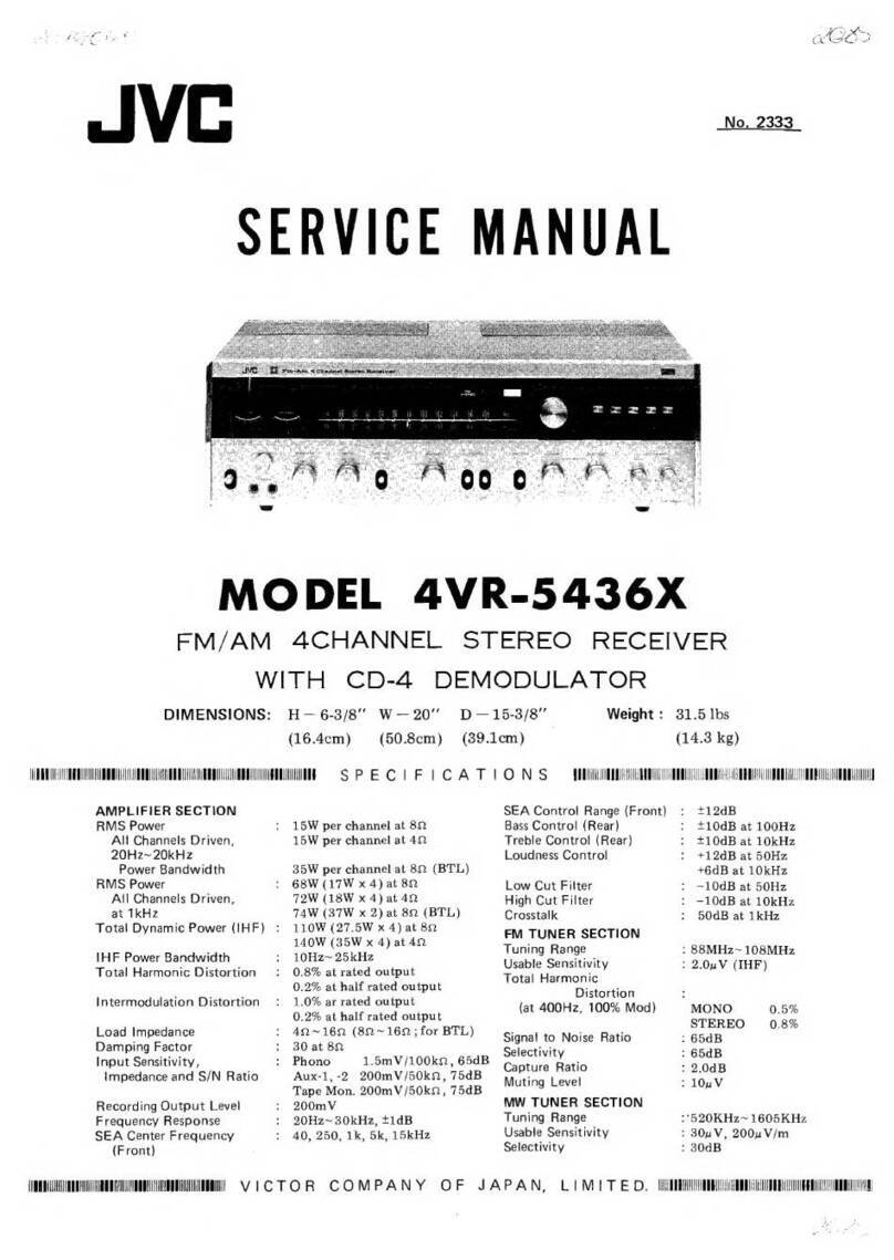
SERVICE
MANUAL
RS77
DIGITAL
SYNTHESIZER
STEREO
RECEIVER
SuperA\
No.
2520
FEB.
1980

Contents
—_
.
Specifications
............
00.
eee eee
2.
Names
and
Their
Functions
2-(1)
FrontPanel............00.00eeee
10.
Printed
Circuit
Board
Ass’y
and
Parts
List
10-(1)
TXX-267
Main
Amp.,
Power
Supply
and
Other
Functions
Split
P.C.
2-(2)
RearPanel..............0-000000s
3
Board
Ass‘y........-----5
10
3.
Removal
Procedures
10-(2)
TXX-268
Equalizer,
S.E.A.
and
Other
3-(1)
Top
Cover
and
Bottom
Plates
.........
4
Functions
Split
P.C.
Board
3-(2)
Power
Transistors
..........0.00005
4
ASS.
sacsps0a
eb
htt
d
dino
ee
ae
13
4.
Main
Parts
Location
10-(3)
TXX-269
Logic
and
Counter
P.C.
Board
4-(1)
Top
View
......
2.2.00
cee
ee
eee eee
5
NSS*Y
eased
a
aby
ae
ae
15
4-(2)
Front
View
...........00
cee
eeee
5
10-(4)
TAP-283
S.E.A.
Control
P.C.
Board
4-(3)
Rear
View......
2...
cece
ee
es
5
ASS
Ye
ea
Ode
GbE
ete
8
17
5.
Exploded
View
and
Part
Numbers
...........
6
10-(5)
TFM-924
FM/AM
Tuner
P.C.
Board
6.
Block
Diagram
of
Digital
Synthesizer
.........
7
ASS'Y
ce
ee
ee
18
7.
Pin-plug
to
Pin-jack
Connections
Diagram
......
7
11.
Accessories
List
.......-...-.-2
02.0
ee
eae
21
8.
FM/AM
Tuner
Alignment
Procedures
12.
Packing
Materials
and
Part
Numbers..........
21
8-(1)
FM
Section
..............20e
000s
8
13.
R-S77
Schematic
Diagram
.........--0
0000s
22
8-(2)
AM
Section............0000ce
eae
9
14.
Parts
List
with
Specified
Numbers
for
9.
Power
Amplifier
Idling
Current
Adjustment
Designated
Areas
.......
0.
0c
eee
eee
eee
24
Procedure
.....
00.0
e
eect
eect
ee ne
eene
9
Warning:
When
replacing
the
parts
marked
with
A\
,
be
sure
to
use
the
designated
parts
to
ensure
safety.
1.
Specifications
FM
Tuner
Section
(Figures
are
based
upon
IHF
Standard)
Tuning
Range
:
*87.9
MHz
—
107.9
MHz
(87.5—108.0
MHz
for
50
KHz
step)
:
10.3
dBf
(1.8
wV/300
Q)
Amplifier
Section
RMS
Power
(Both
channels
driven,
from
20
Hz
to
20
kHz
with
0.005
%
:
60
W
per
channel
at
8
Q2
Usable
Sensitivity
(IHF)
50
dB
Quieting
Sensitivity
Mono
:
14.8
dBf
(3
wV/300
Q)
RMS
Power
:
65
W
per
channel
at
8
Q
Stereo
:
37.2
dBf
(40
uV/300
22)
(Both
channels
driven,
Distortion
at
1
KHz)
Mono
:
0.15
%
(1
kHz)
Total
Harmonic
Distortion
:
0.005
%
at
rated
power
Stereo
:
0.3
%
(1
kHz)
20
Hz
—
20
kHz,
8
Q
Signal
to
Noise
Ratio 0.001
%
at
rated
power
1
kHz,
Mono
:
80 dB
(68
dB,
DIN)
8
Stereo
:
70
dB
(62
dB,
DIN)
Input
Sensitivity/Impedanc
Selectivity
:
80
dB,
+400
kHz
Phono
:
2.5
mV/47
kQ
(65
dB,
300
kHz,
DIN)
Aux
:
180
mV/43
kQ
:
1.0
dB
:
100
dB
at
98
MHz
:
78
dB
at
98
MHz
:
45
dB
at
1
kHz
Capture
Ratio
IF
Rejection
Image
Rejection
Stereo
Separation
:
180
mV/43
kQ
(180
mV/43
kQ,
DIN)
Tape
Play
S.E.A.
Graphic
Equalizer
Center
Frequencies
:
40
Hz,
250
Hz,
1
kHz,
5
kHz
AM
Tuner
Section
and
15
kHz
Tuning
Range
:
*530
kHz
—
1620
kHz
Control
Range
-
£12
dB
(522
kHz—1611
kHz
for
9
kHz
step)
Signal
to
Noise
Ratio
:
Phono
77
dB
:
250
pV/m,
50
uwV
(External
Antenna)
:
50 dB
:
0.5
%
at
10
mV/m
:
63
dB
+10
kKHz(60
dB
+9
kHz,
DIN)
(Note)
*U.S.A.
&
CANADA
(New
IHF
75
cB)
Tape
Play
98
dB
(New
IHF
75
dB)
:
See
page
24
Usable
Sensitivity
(IHF
short-circuited
A
network)
Signal
to
Noise
Ratio
Distortion
Selectivity
Power
Consumption
Design
and
specifications
subject
to
change
without
notice.
Dimensions
and
Weight
Dimensions
Areas
Height
_|
Width
12.0
cm
(4-23/32")
|
48.0
cm
(18-29/32")
|
38.2
cm
(15-1/16”)
11.9
em
(4-11/16")
|45.2
om
(17-13/16”)
|
38.2
om
(15-1/16")
Weight
Depth
Net
10.8
kg
(23.8
Ibs.)
10.6
kg
(23.3
Ibs.)
U.S.A.,
Canada
&
U.S.
Military
Market
All
Other
Countries
R-S77
No.
2520
4

@
POWER
switch
ON:
Press
to
turn
the
power
on.
During
the
first
3
or
4
seconds
after
the
POWER
switch
is
turned
on,
no
sound
will
be
heard
until
you
hear
the
“click”
of
the
relay
operation.
This
is
not
due
to
any
defect
in
the
unit.
The
built-in
power
protection
circuit
operates
to
mute
the
switching
noise
for
speaker
protection.
STAND
BY:
When
the
power
cord
is
plugged
into
an
AC
outlet,
the
STAND
BY
indicator
(5)
lights
to
show
that
the
memory
circuit
is
operating.
As
long
as
this
indicator
remains
lit,
the
preset
stations
are
not
subject
to
cancellation
or
alteration.
The
preset
data
are
maintained
even
in
the
case
of
a
power
failure
or
when
the
power
cord
is
disconnected,
if
the
period
of
non-
applied
power
does
not
exceed
a
couple
of
days.
@@®
TUNING
buttons
Auto
tuning
Up-scanning
button:
When
this
button
is
pressed,
the
tuned-in
frequency
changes
in
the
direction
of
increas-
ing
frequencies.
Use
this
button
to
search
the
upper
frequency
broadcast.
Scanning
(Auto
Tuning)
stops
automatically
when
the
next
FM
(or
AM)
station
is
pulled
in.
This
tuned-in
frequency
is
displayed
digitally
by
the
frequency
indicator.
Even
if
you
continue
to
press
this
button,
scanning
stops
at
some
stations
that
can
be
tuned-in,
but
if it
is
not
your
desired
station,
press
the
Up
button
again.
Press
the
Up-scanning
button
and
then
press
the
Down-
scanning
button
to
select
stations
by
down-scanning.
Down-scanning
button:
Press
to
tune
in
the
direction
of
decreasing
frequencies.
Use
this
button
to
search
the
lower
frequency
station.
Functions
are
identical
with
those
of
the
up-scanning
button.
Note:
Scanning
begins
by
pressing
the
Up
or
Down
button,
re-depressing
it
stops
scanning.
=
2.
Names
and
Their
Functions
2-(1)
Front
Panel
Fig.
1
Manual
tuning
Manual
tuning
is
possible
by
pressing
the
Auto-Manual
scanning
switch
(10).
Pressing
the
Up-Down-scanning
buttons,
the
tuned-in
frequency
changes
in
200 kHz
steps
for
FM
reception
(50
kHz
steps
for
Europe
and
Australia)
or
10
kHz
steps
for
AM
(9
kHz
steps
for
Europe
and
Australia).
Tapping
this
button
changes
the
tuner
step
by
step,
continuous
pressing
(more
than
0.5
sec.)
changes
tuning
in
a
high
speed
scanning
sequence
which
stop
when
released.
@)
Left
and
right
channel
power
indicator
These
LED’s
indicate
the
output
power
in
watts.
The
values
in
watts
are
indicated
per
channel
when
one
pair
of
speakers
having
an
impedance
of
exactly
8
ohms
is
being
driven.
®
STAND
BY
indicator
Lights
when
the
POWER
switch
(1)
is
set
to
OFF
(STAND
BY).
©
Frequency
indicator
The
tuned-in
frequency
is
displayed
digitally.
Four
digits
(kHz)
are
displayed
for
AM
reception
and
five
digits
(MHz)
(for
continental
Europe)
or
four
digits
(MHz)
(for
U.S.A.,
Canada
and
other
countries)
are
displayed
for
FM
reception.
@
MEMORY
indicator
When
the
MEMROY
button
is
pressed,
this
MEMORY
indicator
lights
to
show
that
the
unit
is
ready
to
register
the
preset
station
to
memory.
MEMORY
switch
Press
this
switch
and
the
memory
indicator
will
light
to
show
that
this
unit
is
ready
to
receive
a
memory
setting.
(This
switch
is
a
non-lock
type.)
Pressing
the
station
select
button
while
the
MEMORY
indicator
is
lit
(for
about
5
sec.)
makes
it
possible
to
memorize
the
station
being
received.
When
the
MEMORY
indicator
is
not
lit,
the
memory
function
does
not
operate.
@)
Scanning
indicator
This
green
indicator
lights
when
you
make
auto
or
manual
tuning
with
the
Up
or
Down
buttons
(2),
(3).
R-S77
No.2520

AUTO-MANUAL
SCAN
switch
Press
this
switch
in
for
MANUAL
tuning
and
press
again
to
set
to
the
out
position
for
AUTO
tuning.
@)
SCAN
LEVEL
switch
(LOCAL,
DX)
Normally
this
switch
is
set
to
LOCAL
so
that
scanning
stops
automatically
upon
receiving
only
those
stronger
signals.
1f
you
want
to
scan
all
weak
signal
stations,
set
this
switch
to
DX.
@
Station
select
buttons/Station
indicators
These
buttons
are
used
to
select
one
of
the
preset
stations
or
to
preset
the
station
for
an
individual
chan-
nel.
When
one
of
these
buttons
is
pressed,
the
LED
indicator
on
the
corresponding
button
lights
to
indicate
which
channel
is
in
operation.
If
one
of
these
buttons
is
pressed
when
the
MEMORY
switch
(8)
is
pressed
in,
the
station
which
is
being
received
will
be
‘‘“Memorized”.
One
of
the
station
select
buttons
can
be
used
in
common
for
one
FM
station
and
one
AM
station.
If
you
change
the
mode
from
radio
reception
to
any
other
mode
including
power-off
and
back
to
radio
reception,
the
station
previously
selected
with
the
station
select
buttons remains
tuned
in.
However,
unless
the
station
select
buttons
are
pressed,
station
indicators
will
not
light,
but
the
scanning
indicator
will
light
instead.
eo”.
Poe
PROTECTION
CIRCUIT
US
PAT
WO.
9691627
FM/AM
OPERATION
Presetting
to
selected
station
(FM
or
AM)
1.
Press
the
POWER
switch
to
ON
(
=).
2.
Press
the
source
select
switch
FM
(or
AM)
to
ON
(=).
3.
Tune
to
a
desired
station
by
pressing
the
‘““TUNING”
buttons
for
AUTO
or
MANUAL
TUNING.
4,
Press
the
MEMORY
switch
(
-—
).
(The
memory
indicator
lights.)
5.
Press
one
of
the
station
select
buttons
(=).
6.
Make
the
same
pre-tuning
procedure
(steps
3,
4,
5)
for
the
remaining
channels.
Pre-tuning
is
possible
up
to
12
different
stations
(6
FM
stations
and
6
AM
stations).
7.
Press
the
desired
station
select
button
for
listening
(=).
(This
indicator
on
the
corresponding
button
lights
to
indicate
which
channel
is
in
operation.)
Listening
to
FM
broadcasts
1.
Press
the
POWER
switch
to
ON
(-—).
2.
Select
the
speaker
system
with
the
SPK-1
or
SPK-2
switch.
3.
Press
the
FM
button
to
ON
(=).
4.
Press
the
desired
station
select
button
(=
).
5.
Adjust
the
volume
and
balance
to
your
requirements
and
use
the
S.E.A.
controls
to
obtain
the
tone
you
want
to
hear.
aoe
euecTmOUE
|
eos
meses
cov
POUIANT
ow
Sooo
Eeveer
Aeron
=
FT
a
E
PAR
LUSAGER.
SIDRESSER
A
UN
‘US
PAT
NO.
3566204
eas
PARATEUR
COMPETENT.
CAUTION:
SPEAKER
IMPEDANCE
1A
‘MANUFACTURED
8
|
VICTOR
COMPANY
OF
JAPAN.
LTD.
.
——
®
@
TAPE
DIN
socket
(REC/PLAY)
@
AM
channel
spacing
switch
(Provided
on
sets
for
the
Europe,
Australia
and
U.K.)
@
Voltage
selector
(Not
provided
on
sets
for
U.S.A.,
Canada,
Europe,
Australia
and
U.K.)
@
AC
outlet
(Not
provided
on
sets
for
Continental
Europe,
the
United
Kingdom
and
Australia.)
R-S77
No.2520
(Provided
on
sets
for
the
U.S.A.,
Canada,
etc.
Set
this
switch
according
to
AM
channel
spacing
of
your
country.)
©)
Fuse
holder
(Not
provided
on
sets
for
U.S.A.,
Canada,
Europe,
Australia
and
U.K.)
Note:
@
The
AC
outlet
is
not
switched
off
by
the
front
panel
power
switch.
Connect
it
to
a
component
which
only
uses
power
when
operating,
like
a
record
turntable.
=o

3.
Removal
Procedures
3-(1)
Top
Cover
and
Bottom
Plates
for
U.S.A.,
Canada
and
U.S.
Military
Market
Screw
E23388-002
E65550-003
Serve
(Ueper)
Top
Cover
(Metal)
SBSB3008N
Screw
£65550-002
Goamecte
ad
Screw
(Lower)
(Right)
E65550-003
Screw
(Upper)
ED92940-001
Cosmetic
Board
(Left)
E65550-002
E300819-001
Screw
(Lower)
Bottom
Plate
2
Fig.
3
>
E47227-012
Foot
i
i
Screw
23388-001
7
1
SBSB3008N
Seni
et
§_sBs8301
0z
Top
Cover
(Metal)
Screw
crew
SBSB3008Z
SBSRS0002
E61660-001
Screw Screw
Screw
re
for
All
Other
Areas
eadoend-ooi
Side
Fitting
E300819-001
Bottom
Plate
E61660-001
Screw
E300884-001
Side
Fitting
E300820-001
Bottom
Plate
oe
|
£47227-012
SBSB3008Z
ae
——
Screw
SBSB3008Z
SBSB30102Z
Fig.
4
Screw
Screw
3-(2)
Power
Transistors
©
TXX-267-1
Main
Amp.
P.C.
fi
Board
Ass’y
Front
Panel
@
Heatsink
Rear
Panel
Procedures:
Step
1:
Remove
the
bottom
plate
from
chassis
and
2
screws
@
from
heatsink
@.
Step
2:
Remove
4
screws
@).
Step
3:
Raise
TXX-267
()
from
chassis
as
arrowed
on
Fig.
5
and
then
resolder
the
power
transistor’s
leads.
Step
4:Remove
4
screws
©)
and
heatsink
from
TX
X-267
and
then
replace
the
power
transistors.
@—s
@
Fig.
5
R-S77
a
No.2520

4.
Main
Parts
Location
4-(1)
Top
View
(i
Speaker
Terminal
P.C.
Board
Ass‘y
TXX-267-6
@)Power
Transformer
/\,
See
page
24.
@)
Main
Amp,
P.C.
Board
Ass‘y
TXX-267
D-1
(Refer
to
page
10.)
@
Electrolytic
Capacitor
(8700uF/56V)
QEZ0060-878E
(0
Bar
Antenna
Coil
E03721-009
@)Power
Supply
P.C.
Board
Ass'y
TXX-2670-2
(Refer
to
page
10.)
(@)
FM/AM
Tuner
P.C.
Board
Ass’y
TFM-9240
(Refer
to
page
18.)
@
Shield
Cover
E23466-001
S.E.A.
OFF
Board
Ass‘y
©
Logic
&
Counter
P.C.
Board
Ass‘y
TXX-268-3
TXX-26901-1
oe
=
<
(Refer
to
page
15.)
(@
Power
Indicator
Driver
P.C.
Board
Ass‘y
Fig.
6
TXX-267-4
4-(2)
Front
View
(B
Slide
Knob
(Front
Panel
Ass'y
@Slide
Knob
(@Pushbuttons
Ass’y
E67130-001
See
page
24
E66619-001
E300928-001
R-S77
DIGITAL
SYNTHESIZER
STEREO
RECEIVER
Supe
2\,
SHA
REC
YAMS)
TAPE
2
MOMOVEA
MAHER
LOLIDIMESS
Aun
cone
von
Aa
CaN
EO
"
~
~
a
i"
@)
Pushbutton
Headphone
Jack
Pushbutton Pushbutton
Pushbutton
E66162-001
QMS6302-102
Deer
16-001
E67269-001
©
E67116-001
.
Fig.
7
4-(3)
Rear
View
Q5)
Pin-jack
Ass‘y
Q})
Bar
Antenna
Coil
8
Top
Cover
(Metal)
Rear
Panel
AC
Outlets
A\
Q)DIN
Socket
(4
pins)
E03721-009
See
page
24.
@
See
page
24,
See
page
24
See
page
24.
E03591-41F
EAMUFACTURED
#]
VICTOR
COMPANY
OF
JAPAN,
L10.
TOKYO,
JAPAN,
@Pin-jack
Ass‘y
(4)
Antenna
Terminal
Fuse
Holder/\
AC
Voltage
Selector
@3)
Speaker
Terminal
(22)
Power
Cord
A\
(4
pins)
E03572-021
See
page
24
See
page
24
A
E03572-007EM
See
page
24.
E03591-41F
A :
A\:
Safety
Parts
Qi)
Strain
Relief
A\
See
page
24.
Fig.
8
No.2520
—-5-

100-0993
100-0€
1293
a
qou>
aplis
da
Ps.
100-619993
gouy
apiis
@)
A
on
100-69Z294
Vay
uolinqysnd
@
A
Ngo0easas
one
ma.og
(8)
N800€aS4S
~
masoS(Q)
SF
100-91
1294
uoqnquysnd
LOO-6S7E7C4
A,ss\f
jaued
auos4
Cd)
L00-6S¢z93
alelgq
ag
a
hy
_.
£89OXX1
100-61
1994
A,ssv/
pleog
‘O'd
101e9!pul
G37
110g
@)
Nsooegsas
ma.os
(8)
€697-XXL
A\SSYJ
P12Og
“Dg
YOIIMS
A1owa
Q))
Ns00easas
mags
(8)
Exploded
View
and
Part
Numbers
lee
a
L00-Se600e4
4aP1OH
ans
@))
5.
L00-
197;
_
/S8\V
aseg
1u014
)
LOO-C9L994
V
P1eog
“O'd
EZ
Z
:
.
iA
WK
ss
(WA
OS
Set
Ps
aa
G4
4amog
=
€c4
uolnqysng
yo11Mg
1amog
@)
6
“Big
Nsooegsas
@
G-L97-XXL
Ass
pieog
“O'd
V89TXXL
A,ss\J
pleog
*O'd
|
jouuog
aouejeg
1g
auinjo,
(1d)
e
.
6ZE-O00vVES
daoedg
1104
02)!
ASS
PleOg
*O'd
ee
r
we
Soe
:
LOO-S9vECA
JaplOH
ule
“Q|
ebed
aas
A,SsW/
PseOg
“O'd
Jalunod
7g
91607
@
(7)
yum
paygere
InN
LOO-V9vETA
sjonuog
vas@d)
yee1g
1U0I4
GI)
JONI
101€9!Pu]
4aMOod
Gd)
R-S77
@
S-192-XX1L
Wo1y
@
smaios
p
anoway
$10}291pul
G37]
ey?
BulAoweYy
&
LOT
XKL
A,ss\v
pseog
*D'q
SayoiiMs
Ad
GNVLS
8
Ja>128dS
LL9O@XXKL
Ass
PAkO"”
'O'd
yoer
sauoudpeay
Gd)
€°890-
XXL
LOO-ZZZ2294
yayoeig
adAL
,,1,,Q2)
A,SSW
pueog
“O'd
vas@
ie,
Pad
1OAIY
91184
G0)
Se
AN
4
v7
L9@-XXL
-™
A,ssW¥
pseog
‘O'd
1-89
XXL
A,ss\f7
pseog
‘O'd
Ns00easas
|
ianieisiaind
mass
(8)
No.2520
soyoums
1g
Jazijenby
@§)

Block
Diagram
of
Digital
Synthesizer
EM
EM
1C303
uPB553C
F.L.
Display
Tuning
osc
Woltege
Freq.
|
ECL
1/16.
1/17
Presealer
Li
1%
AM
OSC
Devided
FM
Freq.
OSC
Freq.
-=
AM
.
liramere
Tuning
counter
Voltage
4.5
MHz
SS
X'tal
Resonator
ee
ee
ee
ee
Quatre
Programed
in
osc
FM
6
+
last
CH
Micro
Computer
Freq.
AM
6
+
last
CH
Memory
CH1
—6
key
1C302
uPD1703-011
:
Memory
key
Fig.
10
7.
Pin-plug
to
Pin-jack
Connections
Diagram
TXX-267-6
Speaker
Terminal
P.C.
Board
Ass‘y
TXX-267-2
Power
Supply
P.C.
Board
Ass’y
(See
page
10)
—_
i902
(See
page
10)
——|
vin
TXX-268-2
J801|
Pin-jack
Power
Transformer
P.C.
Board
Ass’y
See
page
24
reo1(
A
—
(See
page
13)
|
f
l
fl fl
f
l
l
|
l
|
=
TXX-267-1
104
P103
TFM-924
Main
Amp.
P.C.
Board
Ass’‘y
(See
page
10)
FM/AM
Tuner
P.C.
Board
Ass‘y
8
3104
2|(]
DY
se02
(See
page
18)
p701
i
[]
[3803
=
en
ee
P901c3
Br
eee
aie
|
TX
X-267-3
TXX-268-1
Speaker
&
STAND-BY
Switch
P.C.
Board
Ass‘y
So
Equalizer
&
Switch
P.C.
Board
Ass’y
R-S77
No.2520
(See
page
11)
—
(See
page
13)
TXX-268-3
SEA
P.C.
Board
Ass’y
TAP-283
_
(See
page
14)
SEA
Control
P.C.
Board
Ass’'y
(a
sama
A
(See
page
17)
fF
Connectors
Table
TX
X-269-1
Ral
TO
Bi
<a
Logic
&
Counter
In-piug
Location
iso
Location
P.C.
Board
Ass’y
Sone!
abeereie)
(See
page
16)P803
P101
TFM-924
J101
TXX-269-1
P102
TFM-924
J102
TXX-269-1
P103
TFM-924
J103
TXX-269-1
P104
TFM-924
J104
TXX-268-1
+TXXD685
P201
TFM-924
J201
TXX-269-1
Seco
:
P301
TXX-269-1
|
J301
TXX-268-5
ee.
Heer
eee
P302
TXX-269-1
|
J302
TXX-267-2
ee
page
Fig.
11
P501
TAP-283
|
J501
TXX-268-5
.
P701
TXX-267-1
|
J701
TX
X-268-3
P801
TXX-267-2
|
J801
TXX-268-1
P802
TXX-267-1
|
J802
TXX-268-3
P803
TXX-367-1
|
J803
TXX-268-1

8.
FM/AM
Tuner
Alignment
er
P102
TC201
om
TC202
T201
IC
201
T202
Procedures
VR101
©
P103
P104
T203
VR102
Alignment
Location
of
TFM-924
FM/AM
Tuner
P.C.
Board
Ass’y
Fig.
12
Frequency
Counter
Loop
Antenna
AM
SSG
3
Receiver
FM
75
2:
75
Q
PAD
Fig.
13
8-(1)
FM
Section
Sensitivity
Low
Frequency
1.
2.
3;
4.
5.
6.
Connect
an
RF
generator
to
the
antenna
terminals
on
the
rear
panel
through
a
dummy
antenna.
Set
an
RF
generator
to
90
MHz,
a
modulation
of
1
kHz
and
a
deviation
of
75
kHz
to
provide
an
input
of
2
uV.
Connect
a
VTVM
and
an
oscilloscope
to
the
Rec.
out
jacks
on
the
rear
panel.
Set
the
frequency
display
to
89.9
MHz.
Adjust
L104
so
that
‘“’V.
TUNE”
-TP116
indicate
3.7
V
by
VTVM.
Adjust
three
coils
L101,
L102
and
L103
in
the
tuning
gang
to
maximize
the
output.
High
Frequency
7.
10.
11.
Set
the
RF
generator
to
106
MHz,
a
modulation
of
1kHz
and
a
deviation
of
75
kHz
to
provide
an
input
of
2uV.
.
Set
the
Frequency
Display
to
105.9
MHz.
.
Adjust
TC104
so
that
‘‘V.
TUNE”
TP116
indicate
18.0
V
by
VTVM.
Adjust
the
FM
trimmers
TC101,
TC102
and
TC103
in
the
tuning
gang
to
maximize
the
output.
Repeat
these
high
and low
frequencies
adjustment
alternately
until
maximum
sensitivity
is
obtained.
Distortion
Meter
Oscilloscope
Descriminator,
Distortion
and
Signal
Gain
w
NOoS
co
.
Press
to
FM
position.
Connect
an
RF
generator,
1
kHz
modulation
and
a
75
kHz
deviation
to
the
antenna
terminals
on
the
rear
panel
through
a
dummy
antenna.
Connect
an
oscilloscope,
Distortion
Meter
and
VT
VM
to
the
Rec.
out
jacks
on
the
rear
panel.
Set
the
RF
generator
to
97.9
MHz.
Set
the
Frequency
Display
to
a
97.9
MHz.
Connect
aDC
VTVM
between
TP111
and
112.
Adjust
the
core
indicated
arrow
A
of
T7101
for
DC
VTVM
reading
of
0
(zero)
mV.
Adjust
the
core
indicated
arrow
B
of
T101
so
that
the
distortion
is
minimized
at
a
value
less
than
0.4
%.
Multiplex
and
Stereo
Separation
Multiplex
1.
Set
the
stereo
signal
generator
as
follows:
400
Hz
modulation
frequency,
7.5kHz
deviation
pilot,
67.5
kHz
main
and
sub
carriers.
Connect
its
output
to
the
RF
generator.
.
Connect
an
RF
generator
to
the
antenna
terminals
through
a
dummy
antenna.
.
Connect
a
VTVM,
an
oscilloscope
and
a
distortion
meter
to
the
Rec.
out
jacks
on
the
rear
panel.
Set
the
RF
generator
to
97.9
MHz
and
output
of
1
mV.
Set
the
frequency
display
to
97.9
MHz.
.
Connect
the
frequency
counter
to
19
kHz
Test
Point
(TP110).
Switch
off
the
pilot
signal
of
stereo
modulator.
Adjust
VR103
so
that
the
frequency
counter
indicates
19
kHz
(0
~
-50
Hz).
Stereo
Separation
9.
10.
11.
12.
13,
Switch
the
selector
of
stereo
modulator
to
left
channel
modulation.
Adjust
VR102
so
that
the
output
of
right
channel
is
minimized.
Switch
the
selector
of
the
modulator
to
right
channel
modulation.
Adjust
VR102
so
that
the
left
channel
is
minimized.
Set
VR102
to
a
average,
if
the
separation
of
left
and
right
is
different.
R-S77
No.2520

Muting
Level
Note:
No
adjustment
is
necessary.
However,
if
the
check-
up
is
required,
take
the
following
steps.
1.
Release
the
MONO/FM
MUTE
OFF
pushbutton
during
this
adjustment
procedures.
2.
Connect
a
VTVM
and
an
Oscilloscope
to
the
Rec.
out
jacks
on
the
rear
panel.
3.
Set
the
RF
generator
to
108
MHz,
a
modulation
of
1
kHz
and
a
deviation
of
75
kHz,
to
provide
an
input
of
8uV.
4.
Turn
VR101
clockwise
and
remember
the
point
(or
position)
at
which
the
muting
ceases
operating.
5.
Turn
VR101
counterclockwise
slightly
so
that
the
out-
put
level
drops
by
1
dB.
6.
Attenuate
the
output
of
the
RF
generator
to
2
dB
from
8
uV
of
step
2
and
check
that
the
muting
is
still
oper-
ating.
8-(2)
AM
Section
Tracking
and
Sensitivity
Low
Frequency
1.
Press
to
AM
position
2.
Connect
the
RF
generator
to
the
antenna
terminals
on
the
rear
panel,
set
this
to
600kHz
(603
kHz)
with
30
%modulation
at
400
Hz.
3.
Connect
an
AC
VTVM
and
an
Oscilloscope
to
the
Rec.
Out
jacks
on
the
rear
panel.
4.
Set
the
frequency
display
of
the
unit
to
600
kHz
(603
kHz).
5.
Adjust
T201,
T202,
T203
and
the
ferrite
bar
antenna
adjusting
the
coil
to
maximize
the
output
signal.
High
Frequency
6.
Set
the
RF
generator
to
1400
kHz
(1404
kHz)
with
30
%modulation
at
400
Hz.
7.
Set
the
frequency
display
of
the
unit
to
1400
kHz
(1404
kHz).
8.
Adjust
the
trimmers
TC201,
TC202
in
the
tuning
_
gang
so
that
the
output
signal
is
maximized.
9.
Repeat
these
high
and
low
frequencies
adjustment
procedures
alternately
until
maximum
sensitivity
is
obtained.
9.
Power
Amplifier
Idling
Current
Adjustment
Procedure
R738
Right
channel
Adjustment
Location
of
TX
X-267
[_]-1
Main
Amp.
P.C.
Board
Ass’y
Precaution:
(1)
Allow
the
set
to
warm
up
at
least
5
minutes
before
connecting
aDC
VTVM.
(2)
Must
keep
the
heatsinks
cooling
to
prevent
overheating
and
consequent
destruction
of
the
semiconductor
junction
and
set
the
volume
control
to
minimum
during
these
adjustment
procedures.
(_):
for
Right
channel
Adjustment
R-S77
No.2520
Fig.
14
Procedures:
1.
Turn
R737
and
(R738)
fully
counterclockwise
before
the
power
switch
on.
2.
Connect
a
DC
VTVM
to
the
Test
Point
L-CH
and
L-E
(R-CH
and
R-E).
3.
Adjust
R737
(R738)
for
DC
VTVM
reading
of
5
mV.

10.
Printed
Circuit
Board
Ass‘y
and
Parts
List
10-(1)
TXX-267
Main
Amp.,
Power
Supply
and
Other
Functions
Split
P.C.Board
Ass’‘y
The
number
of
TXX-267
[__]
P.C.
Board
Ass’y
varies
according
to
the
area
employed.
Refer
to
page
24.
:
6
a
x)
z
Fig.
15
Each
Individual
P.C.
Board
Location
Fig.
16
Note
(1):
The
specific
symbols
(
#,
2,
&,...
etc.)
on
a
surface
of
above
P.C.
Board
are
actually
unrelated
to
the
repair
service
and
are
significant
denotement
in
order
to
process
the
proper
assembly
of
P.C.
Board
at
the
factory.
Transistors
[item
No.|Part
Number
X701
|2SC1775AV(F1)
|
0.
X702
|2SC1775AV(F1)
X703
|2SC1775AV(F1)
X704
|2SC1775AV(F1)
X705_
|2SC1775AV(F)
|Description
2W
|
200
MHz|Silicon
|
Hitachi
Rating
Oe
@
TXX-267(-J-1:
Main
Amp.
P.C.
Board
Ass‘y
@
TXX-267(]-2:
Power
Supply
P.C.
Board
Ass'y
@®
TXX-267-3
:
Speaker
STAND-BY
Switch
P.C.
Board
Ass’y:
@
TXX-267-4
—
:
Power
Indicator
Driver
P.C.
Board
Ass’y
@®
TXX-267-5
:
Power
Indicator
LED
P.C.
Board
Ass’y
©
TXX-267-6
—:
Speaker
Terminal
P.C.
Board
Ass’y
@
TXX-267-7
:
Headphones
P.C.
Board
Ass’y
TXX-267
(11-8:
AC
Fuse
&
Outlet
P.C.
Board
Ass’y
Note
(2):
In
[_]
should
be
indicated
an
area
code
according
to
the
table
below
before
placing
an
order.
TXX-267
[A]
-1,
-2,
-8
TXX-267
[B]
-1,
-2,
-8
U.K.
TXX-267
-1,
-2,-8
Australia
&
Europe
TXX-267
[D]
-1,
-2,
-8
U.S.
Military
Market
&
Other
Countries
|
TXX-267
[C]
-1,
-2,
-8
Transistors
tem
No.|Part
Number
2S8C1775AV(F)
2S$A949(0,Y)
2S$A949(0,Y)
2SA949(0,Y)
2$A949(0,Y)
R-S77
No.2520

Transistors
Diodes
Item
No,
Part
Number
Rating
Description
Item
No./Part
Number
Rating
Description
Pc
*T
Maker
Maker
all
X711
|2SA1029(C)
0.2W
|
200
MHz|
Silicon
|
Hitachi
D855
=
|SLB-26GG
LED
Toyo
Dengu
X712
|2SA1029(C)
bd
=
D856
|SLB-26GG
" “
X713
|2SC2229(0,Y)
0.8W
|120MHz}
”
Toshiba
D857
+|SLB-26GG
”
”
X714
|2SC2229(0,Y)
"
“a
ti
7
D858
‘|SLB-26GG
=
i”
X715
|2SC2546(E)
04W
|90MHz]}
"
Hitachi
D859
|SLB-26GG
"
ze
X716
|2SC2546(E)
a
mt
o
i
D860
|SLB-26GG
ne
7
X717
|2SC1775AV(F)
|0.2W
|
200MHz!
”
"
D861
|SLB-26GG
7
y
X718
|2SC1775AV(F)
7 a
“
D862
|SLB-26GG
7 "
X719
|2SA872AV(E)
0.3W
|
120MHz|
”
"
D863
|SLB-26GG
ad
“
X720
2SA872AV(E)
|
" a
d
"
D864
_
|SLB-26GG
a
Y
X721
|2SD669A(B,C)
|20W
|
140MHz}
" "
D865
|SLB-26GG
" "
X722
|2SD669A(B,C)
”
.
a
7
D866
|SLB-26GG
7
.
X723
|2SB649A(B,C)
=
os
ve
|
wt
D867
|1S2076-31
Silicon
|
Hitachi
X724
|2SB649A(B,C)
,
"
7
7
D868
|1S2076-31
a
7
X725
|2SD845LB(R,O)
|
120
W
|
20
MHz
da
Toshiba
D869
_
|1S2076-31
ad
‘a
X726
[2SD845LB(R,0)
|
” "
o
Ze
D870
|1S2076-31
.
.
X727
|2SB755LB(R,0){
”
.
"
"
bs
1S2076-31
" m
X728
|2SB755LB(R,0)
at
a
7
D902
|1S2076-31
"
is
X801
|2SD313V(D,E)
|30W
|8MHz
ee
Sanyo
X802
|2SB507V(D,E)
X803
|2SD313V(D,E)
-
" 7
o
Coils
X804
|2SC1775AV(F)
|0.2W
|
200MHz|
”
Hitachi
:
”
Item
No.|Part
Number
Rating
Description
X805
|2SD313V(D,E)
|30W
|8MHz
Sanyo
L701
|E04059-1R0
Choke
Coil
X901
|2SC1775AV(F)
|0.2W
|
200MHz|
”
Hitachi
X902
|2SC1775AV(F)
.
i‘
"
"
X903
|
2SA872AV(F)
0.3W
|
120MHz|
”
"
L702
_
|E04059-1RO
Integrated
Circuits
apache
Parton
Item
No,
Part
Number
Rating
Description
art
Sumber
C701
|QET61HR475zZ
[4.7
uF
[50V_
|
Electrolytic
pte
C702
|QET61HR475z|
” z
a
Ree
Cc.
C705
|QFM31HK-392Z|3900pF|
”
|
Mylar
BAGEE
C707
|QET61CR-107Z
|
100
uF
|16V_
|
Electrolytic
C708
|QET61CR-107zZ|
”
as
at
C709
|QFM31HK-272Z|
2700
pF
|50V_
|
Mylar
C710
|QFM31HK-272z|
“
7
C711
|QCS31HJ-120Z
|
12
pF
i
Ceramic
Diodes
C712
|QCS31HJ-120zZ
|
”
C713
|QCS22HJ470
|47pF
|500v|
”
C714
|QCS22HJ470
Z 2
7
C715
|QCS22HJ-470
“
a
a
C716
|QCS22HJ-470
ie
" a
C717
|QFM31HK-473Z|
0.047
uF/50
V_
|
Mylar
c718
|QFM31HK473z|
“”
" ”
C801
|QEZ0060-878E
|8700uF|56V_
|
Electrolytic
C802
|QEz0060-878E
|
”
a
"
C803
|OQFM32AK-104
|0.1uF
|100V
|
Mylar
C804
|QCE22HP-103
|
0.01
uF
|500
V
D709
|1S2076-31
C805
_|QCE22HP-103
|
”
"
D710
|1S2076-31
C806
|QFM32AK473
|
0.047
uF/100
V |
Mylar
D801
|30D2FA-S
Nihon
Inter
A\
C807
|QFM32AK473
|
“ . 7
”
o
”
Part
Number
D701
|1S2076-31
D702
|1S2076-31
D703
|
1S2076-31
D704
|1S2076-31
D705
|
1S2076-31
D706
|
1S2076-31
D707
|
1S2076-31
D708
|1S2076-31
D802
|30D2FA-S
A
C808
|QET51VR-227
220
uF
|35V
Electrolytic
D803
|30D2FA-S
A
C809
|QET51VR-227
re
ds
"
D804
|30D2FA-S
A
C811
|QET51CR-227
i
16V
-
D805
|RD30EB3
Silicon
|NEC
C812
|QCF31HP-103Z
|
0.01
uF
|50V_
|
Ceramic
|
(Zener)
C813
|QET51CR-228
|
2200uF/16V_
|
Electrolytic
D807
|RD15EB3
" "
C815
|
QCF31HP-2232
"
"
:
Ds0g
_|RD15EB3
” ”
C816
|QET61AR-227Z
|
220uF
|10V_
|
Electrolytic
D811
|RD13EB3
td
*
C851
|QET61ER-106Z
|
10
uF
25V
a
D812
|ERB12-02RKL1
Silicon
|
Fuji
A
C852
|QET61ER-106Z
|
”
.
i.
D813.
|ERB12-02RKL1
7
7
A
C853
|QET61HR-225Z
|2.2uF
|50V
a
psi4_
|ERB12-02RKL1
”
”
A
C854
|QET61HR-225Z2]
”
"
.
D815
|ERB12-02RKL1
”
"
A
C901
|QCF31HP-223Z
|
0.022
pF
Ceramic
D816
|RD6,
2EB3
Silicon
|NEC
C902
|QCF31HP-223Z
|
” “ ”
(Zener)
C903
|QET61HR-226Z
|
22
uF
7
Electrolytic
D851
_
|SLB-26GG
LED
Toyo
Dengu
C904
|QET61AR-107Z|100uF
|10V
a
D852
|SLB-26GG
i
|
”
"
C905
|OQET61CR-226Z
|
22
uF
16
V
<
D853
|SLB-26GG
”
"
C906
|OQET61HR-105Z
|
1
uF
50
V
ig
D854
_
|SLB-26GG
|
me
iad
C999
_
|
OCF31HP-1022
|
1000
pF]
”
Ceramic
|
R-S77
No.2520
-11-

Resistors
Resistors
Item
No.|Part
Number
Rating
Description
|
Item
No./Part
Number
Rating
Description
R001
|QRC121K-275EM|2.7
MQ
|
1/2W
|
Composition
/\
R804
|QRD129J472
4.7kQ
|
1/2W
|
Carbon
7
R701
|QRD141J-222SY
|2.2kQ
|
1/4W
|
Carbon
R805
j/QRD129J-151
150
2
"
a
L\
R702
|ORD141J-222SY
|
”
‘a
ee
R806
|QRD129J-151
sd
a
oe
LAN
R703
|ORD141J-473SY
|47
kQ
ae
7
R807
|QRGO17J-152S
|1.5kQ
|1W
Oxide
Metal
FilmA\
R704
|ORD141J473SY
|
_"
er
is
|
R811__|QRGO27J-680
68
2
2W
fi
R705
|QRD149J-102S
|1kQ2
id
Carbon
Z\
R812
|QRGO17J-330S
|332
1W
"
A
R706
|QRD149J-102S
"
-
a
JN
R813
|QRD129J-392
3.9kQ
|1/2W
|
Carbon
A\
R707
|QRD149J-102S
7
7
i
AN
R814
|QRD149J-101S
|1002
1/4W
7
AN
R708
|QRD149J-102S
*
ue
/N\
R815
|QRD129J6R8
|6.82
1/2W
ud
LN
R709
JORD149J-220S
222
ue
ee
ZN
R816
|QRD149J-102S
|1kQ
1/4
wie
a
AN
R710
|QRD149J-220S
-
"
"
AN
R817
|QRD141J-821SY/820
2
ue
Carbon
R711
|QRD149J-220S
ne
us
se
aN
R818
|QRD141J682SY
|
6.8
kQ
ue
%
R712
|QRD149J-220S
“ i
ie
AN
R831
|QRD141J-471SY|470
ur
”
R713
|QRD149J-150S
|150
=
a
LAN
R852
|ORD141J-332SY
|
3.3
kQ
u
ue
R714
|QRD149J-150S
"
uf
dé
ZN
R853
|QRD141J-390SY
|
39
2
a i
R715
|jJQRD149J-301S
|300
2
-
"
AN
R854
|QRD141J-390SY|
”
ue
ae
R716
|QRD149J-301S
”
ae
x
oe
A
R855
|QRD141J-103SY
|
10
kQ
n
~
R717
JQRD141J-223SY
|22
kQ
m
Carbon
R856
|QRD141J-103SY|
”
um
id
R719
jJQRD149J-220S
|220
a
Carbon
Z\
R857
|QRD141J473SY
|
47
kQ
nf
ue
R720
|QRD149J-220S
ye
m
a
LN
R858
|OQRD141J473SY|_
”
uy
"
R721
|jJQRD149J-100S
|102
- i
LN
R899
|See
page
24
2:72
1/2W
"
R722
|j|QRD149J-100S
7
=
"
AN
R901
|QRD141J-222SY/}2.2kQ
|
1/4W
R723
|QRD149J-100S
a
um
a
A
R902
|ORD141J-222SY|)
”
u
Kd
R724
|QRD149J-100S
- o
ye
uN
R903
{/ORD141J-102SY]1kQ
w
R725
|QRD141J-132SY
|1.3
kQ
a
Carbon
R904
/ORD141J-102SY|
” "
iB
R726
|QRD141J-132SY|
”
”
a
R905
|QRD141J-123SY
|
12
kQ
"
ny
R727
|QRGO17J-822S
|8.2k2
|
1W
Oxide
Metal
FilmZ\
R906
|OQRD141J-123SY)
"
7
és
R728
|QRGO17J-822S
m
di
a
AN
R907
|QRD141J-103SY
|
10
kQ
"
ds
R729
|QRDT49J-181S
|180
2
1/4W
|
Carbon
ZA\
R908
|QRD141J-332SY
|
3.3
kQ
ab
me
R730__|QRD149J-181S
u
_
id
LN
R909
|ORD141J-683SY
|
68
kQ
m
am
R731
|ORD149J-561S
|560
2
.
"
R910
|QRD141J-563SY
|
56
kQ2
.
u"
R732
|QRD149J-561S
a
"
"
A
R911
|QRD141J-183SY
|
18
kQ
ue
as
R733
QRD129J-473
47
kQ
1/2
W_
|
Carbon
AN
R912
|ORD141J-683SY
|
68
kQ
a
aa
R734
|QRD141J-473SY
|
"
1/4W
|
Carbon
R913.
|ORD141J-153SY|
15
kQ
”
”
R735
|ORD149J-181S
|180
2
=
Carbon
/\
R914
|OQRD141J-204SY
|
200
kQ
" "
R736
|QRD149J-181S
ue
-
"
JN
R915
|QRG027J681
680
Q
2W
Oxide
Metal
Film/\
R737
|QVZ3501-471
470
2
Variable
R916
|QRD129J-271
270
2
1/2W
|
Carbon
R738
|QVZ3501-471
ad
y
R917
|QRD141J-223SY
|
22
kQ
1/4W
|
Carbon
R739
|QRD141J-471SY|
"
1/4W
|
Carbon
R918
|ORD141J-104SY
|
100
kQ
7
"
R740
|QRD141J-471SY|_”
=
ad
R919
|QRD141J-104SY|
” 7 ”
R741
|SDT35
350
2
1W
Thermistor
R920
|QRD141J-104SY;
"
sh
ee
R742
|SDT35
"
ue
e
R921
|QRD141J-563SY
|
56
k2
sf is
R743
J|QRD141J-391SY
|390
2
1/4W
|
Carbon
R951
|QRGO17J-221S
|2202
1W
Oxide
Metal
FilmZ\
R744
|QRD141J-391SY|
”
ad
id
R952
|QRGO17J-221S
w
is
ti
AN
R745
|QRD141J-243SY
|24
kQ
P
a
R953
|QRD141J-332SY/3.3kQ
|
1/4W
|
Carbon
[R746
|ORD141J-243S8Y|
”
a
id
R954
|QRD141J-332SY|)
"
ue a:
R747
|QRD149J-122S
|1.2kQ2
re
Carbon
Z\
R955
|QRD141J-681SY|
680
2
ne
um
R748
|QRD149J-122S
"
ue
a
AN
R956
|QRD141J-681SY|
”
a
un
R749
|QRD149J-101S
|100
2
”
m
A
R750
|ORD149J-101S
|
”
ff
id
ZN
A
R751
|ORD149J-100S
|102
"
"
R752
|QRD149J-100s
|
”
ZN
R753
|ORD149J-100s
|
” a
Z
A
AN
R754
|QRD149J-100S
a
ie
"
Others
R755_|ORMOS4K-R22
|0.22
2
|
5W___|
Metal
Plate
=
Item
No.|Part
Number
Rating
Description
__|
R756
|QRMOS4K-R22
|
”
"
i
QMC0437-001
AC
Outlet
A\
IGT:
OIMOORR
22
.
:
rn
J901
|ams6302-102
Headphones
Jack
R758
|ORMOS4K-R22
P701
JQMV5005-003
3-pins
Plug
Ass’y
R759
|ORD149J4R7S
[4.72
|1/4W
|
Carbon
A\
pani
lan
se05-006
Spine
Plug
Aés'y
R760
|QRD149J-4R7S
id
id
ia
aS
|
P802
j|QMV5005-002
2-pins
Plug
Ass’y
|
R761
|See
page
24
102
|1W_
|
Oxide
Metal
FilmA\
meng
lONK/SOOR0GS
a
wins
Pig
Ay
R762
See
page
24
" "
"
A
P901
JQMV5005-003
"
R801
|QRGO17J-680S
|68
2
‘
AN
=67275-001
camieeket
R802
|ORGO1
74-6808
" i
A
swg901
|QSP0020-001E
Push
Switch
R803
|ORD129J472
|4.7k2
|
1/2W
|
Carbon
A
nvddd
BeKepe4-o13
Belay
Switch
E03572-007EM
Speaker
Terminal
£300932-001
LED
Holder
E300934-001
Heat-sink
E60171-003
7
SW902,|QSP0229-019
Push
Switch
903
R-S77
—12—
No.2520

10-(2)
TXX-268
Equalizer,
S.E.A.
and
Other
Functions
Split
P.C.Board
Ass’y
The
number
of
TXX-268
[_]
P.C.
Board
Ass’y
varies
according
to
the
area
employed.
»
TI
TIS
TIR
—
R2R’
R2G)(R2L)T2R
TXx-268
[AB]
:
GAUTION-
x0
PREVENT
ELECTRICAL
SHOCK,DO
NOT
REMOVE
COVERS
(OR
CABINET).NO
USER-SERVICEABLE
:
PARTS
INS
isioe.
REFER
SERVICING
TO
QUALIFIED
SERVICE
Each
Indivudual
P.C.
Board
Location
®
@
TXX-268-1
—:
Equalizer
and
Switch
P.C.
Board
Ass’y
@
TXX-268
[[]-2:
Pin-jack
P.C.
Board
Ass’y
@®
TXX-268-3
__:
S.E.A.
(Sound
Effect
Amp.)
P.C.
Board
Ass‘y
@®
TXX-268-4
—
:
Balance
Control
P.C.
Board
Ass’y
®
TXX-268-5
:
LED
Indicator
P.C.
Board
Ass‘y
Note
(2):
Fig.
18
In
[_]
should
be
indicated
an
area
code
according
to
table
below
before
placing
an
order.
Note
(1):
7
The
specific
symbols
(
#,
2,8,
...
etc.)
on
a
surface
of
above
P.C.
Board
Ass’y
U.S.A.,
Canada,
U.S.
Military
Market
and
|
TXX-268[A]
-2
Other
Countries
U.K.,
Australia
and
Europe
TXX-268
2
P.C.
Board
are
actually
unrelated
to
the
repair
service
and
are
significant
denotement
in
order
to
process
the
proper
assembly
of
P.C.
Board
at
the
factory.
Transistors
Diodes
[item
No|[Part
Number
|
Rating
___[Deseription
Maker
Toyo
Dengu
trem
NoPart Number
_{
__Fating
__|Deseription
—__]
pee
|
tr
2SA872AV(E)
2SA872AV(E)
28C1775AV
(F)
2SC1775AV(F)
2SD438(D,E)
2SD438(D,E)
Integrated
Circuits
Item
No.|Part
Number
Rating
Description
HA1457
1C502_
|HA1457
Ic
um
Hitachi
1S2076-31
R-S77
No.2520
_13—

Capacitors
Resistors
Item
No.|Part
Number
Rating
Description
[Item No.
|Part
Number
|
Rating
Description
C401
|QET61HR475z
14.7nF
|50V_
|Electrolytic
R413
|ORD141J-331SY|3309
|1/4W
|
Carbon
C402
/QET61HR475z
|
” "
if
R414
|ORD141J-331SY|
” a
7
C403
|OETG6OJR-227Z
|220uF
|63V
|
"
R415
|QRGO17J-222S
|2.2k2
|1W_
|
Oxide
Metal
Film
C404
jQET6OJR-227Z
|
" . ‘
R416
|ORGO17J-222S8
|
”
te
"
C405
|QCS31HJ-101Z
|
100
pF
|50V_|Ceramic
R417_|ORD141J-224SY
|220
kQ
|1/4W_|
Carbon
c406
|OCS31HJ-101zZ
|
”
“e as
R418
|ORD141J-224SY|
”
7 z
C407
/QCS31HJ470Z
|
47
pF
7 ”
R419
|ORD141J-153SY
|
15
ka
“
ae
c408
|OCS31HJ470zZ
|
”
a "
R420
|ORD141J-153SY|
” 7
7
C409
|QETG6GOJR-227Z
|220uF
|6.3V_
{Electrolytic
R421
|ORD141J-224SY
|220
kQ
"
”
C410
|QET6OJR-2272
|”
.
°
R422
|ORD141J-224SY|_"
e
us
C411.
[OFM31HK-153Z
[0.015
uF/50V_
‘|Mylar
R423
|ORD149J-560S
[562
a
aN
C412
|QFM31HK-153zZ|
”
7 a
R424
|ORD149J-560S
|
” e
ca
AN
C413.
|QFM31HK-472Z|4700
pF
|
”
i
R441
|ORD141J-334SY]330kQ
|
” "
C414
|QFM31HK-472Z|
"”
ie
ms
R442
|ORD141J5-334SY|
”
"
»
(
TXX-268B-2
C415
|jQCS31HJ471Z
|
470
pF
"
Ceramic
R443
|ORD141J-104SY
|
100
kQ
" 1
{
only
c416
l|Ocs31HJ471z
|
”
7
"
R444
_|ORD141J-104SY|_”
a "
C417
|QEZ0046-105
|
1uF
”
Electrolytic
R451
|ORD141J-332SY|3.3kQ
|
” ”
C418
|QEzZ0046-105
"
"
a
R452
|ORD141J-332SY|
" 7
a
C419
JOQET61HR-476Z
|
47
uF
- ”
R453
|ORD141J-332SY|
" ”
"
C420
[QETEIHR476Z
|"
af
.
R454
|ORD141J-332sY|
”
"
re
C441
|OCF31HP-223Z
[0.022
uF]
”
Ceramic
R455
|ORD141J-564SY|560kQ
|
”
a
C442
|OCF31HP-103Z
|0.01uF
|
”
7
R456
|ORD141J-564SY|
” Z
z
C443.
|OCF31HP-103Z
|
”
is
iu
R457
|ORD141J-223SY
|
22
kQ
ie
i
C444
|OCF31HP-103Z
|
i
.
R458
|ORD141J-223SY|
“ 7
a
C451
|QCS31HJ-2712
|
270pF
|"
.
R459
|ORD141J-564SY|560kQ
|
”
te
C452
|OQCS31HJ-271Z
|
” Z a
R460
|ORD141J-564SY|
”
z
z
|
C453.
|QFM31HK-273
|0.027uF|
”
Mylar
R471
|ORD141J-681SY
|680
2
a
i
C454
|QFM31HK-273
|
” i "
R472
|ORD141J-102SY
|
1
k2
“i
’
C455
|QFM31HK-822
|0.0082uF|
”
"
R473
lornD141J-1028Y|
"
"
a
C456
|OFM31HK-822
|
” e .
R474_|QRD141J-102SY|_"
*
is
_
—
_
—
—
R475
|ORD141J-221SY|220
2
aa)
C531
|QET61HR475z
|4.7uF
|50V
"
—
=
=
=
=
C532
|OET61HR475z]
”
=
=
_
=
=
C533
|OET61AR476Z
|
47
uF
R506
|QVT9C2B-5G5E
|
150
k(B)
Variable
C534
|QET6IAR476Z
|
”
R507_|QVT6C2W-6F5_|
250
k(W)
at
_|
C535
|OCS31HJ-101Z
|100pF
|50V_
[Ceramic
R551
|ORD141J-184SY|180
kQ
[1/4W
|
Carbon
C536
|QCS31HJ-101Z
|
”
vs
‘
R552
|ORD141J-184SY|
a
C537
|QET61AR-476Z
|47
uF
|10V_
|Electrolytic
R553
|ORD141J-102SY|1k2
ie
7
C538
|QET61AR476Z
|
"
“ "
R554
|ORD141J-102SY|
”
"
"
C539
+|QCS31HJ-820Z
|
82
pF
50
V
Ceramic
R555
+
|ORD141J-222SY
|
2.2
kQ
"
"
C540
|OCS31HJ-820z
|
” a z
R556
|ORD141J-222SY|
”
z
a
C541
|OQCS31HJ-560Z
|
56
pF
‘a
i
R557
|ORD141J-682SY|6.8kQ
|
”
e
C542
|QCS31HJ-560Z
|
"
a‘
iD
R558
|ORD141J-682SY|
“
‘i
‘
C543
|OCS31HJ-271Z
|
270pF
|
"
.
R559
|ORD141J-103SY|
10
k2
a
a
C544
|QCS31HJ-271Z
|"
.
‘-
R560
_|ORD141J-103SsY|_”
2
‘
c545
|OEz0046475
=|
4.7
uF
ae
Electrolytic
R561
|ORD141J-562SY|/5.6kQ
|
”
z,
C546
|QEZ0046-475
”
Z
it
R562
j|ORD141J-562SY|
“
i "
C547
|QET61ER476Z
[47uF
|25V
"
R563
|ORD141J-102SY]
1
kQ
"
7
|
C548
|OET6IER-476Z
|
R564
pemiaiianay
|.
&
e
[2
Resistors
Others
Item
No.|/Part
Number
Rating
Description
Item
No.
Part
Number
Rating
Description
R401
/ORD141J-222SY|
2.2
ka
[1/4
w
Carbon
TP104
|EWso1B-001
11-pins
Socket
Ass’y
|
R402
|ORD141J-222SY|
”
Z
”
TP301
|EWSO18-013
8-pins
Socket
Ass’y
R403
|QRD141J-563SY|
56
ka
7
a
TP501
|EWSO17-016
7-pins
Socket
Ass’y
R404
|QRD141J-563SY|_”
a “
TP701
|EWSO13-046
3-pins
Socket
Assy
R405
|QRD141J-271SY|
270
2
-
e
TP801
|EWSO015-024
_|5-pins
Socket
Ass’y
R406
|ORD141J-271SY|
"
"
a
TPg02
|EWS012-031
2-pins
Socket
Ass’y
R407
|ORD141J-224SY|
220k2
|
”
TPg03
|
Ewso13-036
3-pins
Socket
Ass’y
R408
/ORD141J-224SY|
”
”
“i
TP901
|EWS013-037
a
R409
|ORD141J-473SY]
47
k2
” a
£03591-42D
4-pins
Jack
Ass’y
R410
|ORD141J473SY|
"
7
es
E03623-003
DIN
Socket
R411
|QRD141J-392SY|
3.9
k2
u
ie
(TXX-268B-2)
R412
|ORD141J-392SY|
i”
fe
|
(s)
E300930-001
LED
Holder
R-S77
—14-
No.2520

10-(3)
TXX-269
Logic
and
Counter
P.C.Board
Ass’y
The
number
of
TXX-269
[_]P.C.
Board
Ass’y
varies
according
to
the
area
employed.
(,
P-N71-HB
Each
Indivudual
P.C.
Board
Location
a
®
Note
(1):
The
specific
symbols
(
#,2,8
,
P.C.
Board
are
actually
unrelated
to
the
repair
service
and
are
significant
denotement
in
order
to
process
the
proper
assembly
of
P.C.
Board
at
the
factory.
Transistors
Part
Number
Description
Fig.
20
...
etc.)
on
a
surface
of
above
X301
|2SC458(C,D)
0.2W
Hitachi
X302
|2SC458(C,D)
" z
uF
ie
X303
|2SC458(C,D)
tf
te
a 7
X304
|2SC458(C,D)
4
te
X310_|28C458(C,D)
|”
ue
x
"
X311
|2SC458(C,D)
g
ae
7
“
X312
|2SA1029(C,D)
o
200
MHz|
“ "
X313
|2SA1029(C,D)
”
ut
"
iE
X320
|2SK105(F)
0.25
W
F.E.T.
|
NEC
X321
|2SC458(D)
0.2W
|
230
MHz|Silicon
|
Hitachi
X340
|2SC458(C,D)
a a
"
X341
|2SC458(C,D)
a
us
"
X342
|2SC458(C)
a
D "
i
X343
|2SC458(C)
”
“
"
”
[_X350_|2SA872AV(D,E)
|0.3W
|120MHz|_”
”
R-S77
No.2520
S
‘amor
ar
LS
va
RAGA
WAR!
BNe
(77
she
8
SW
3045)
5
o
SW.
305
GBS)
Heo
wn
Tegel
©
Fig.
19
@
TXX-269
[]-1:
Logic
and
Counter
P.C.
Board
Ass‘y
@
TXX-269-2
__:
Preset/Station
Select
Switch
P.C.
Board
Ass‘y
@
TXX-269-3
:
Memory
Switch
P.C.
Board
Ass‘y
@®
TXX-269-4
:
Up/Down
Switch
P.C.
Board
Ass‘y
®
TXX-269-5
:
9
kHz/10
kHz
Select
Switch
P.C.
Board
Ass’y
Note
(2):
In
[_]
should
be
indicated
an
area
code
according
to
table
below
before
placing
an
order.
P.C.
Board
Ass’y
TXx-269[A]-1
U.S.A.,
Canada
and
U.S.
Military
Market
U.K.,
Australia,
Europe
and
Other
Countries
|
TX
X-269
[B
]-1
Transistors
[Item
No.|PartNumber
[Rating
[Description
[
Pe
|
fT
|
He
MHz
|
Silicon
|
Hitachi
Sanyo
NEC
2SA872AV(D,E)
2SA872AV(D,E)
2SA872AV(D,E)
2SA872AV(D,E)
Integrated
Circuits
Toshiba
Hitachi
Toshiba
HD74LS42P
TC4035BP
"
—~15—

Diodes
Resistors
Item
No.|Part
Number
Rating
Description
Item
No.|Part
Number
Rating
Description
ae
|
Maker
R307
|QRD141J-153SY
}15
ka
1/4.W
|
Carbon
‘|
D310
|1S2076-31
Silicon
|
Hitachi
R308
|QRD141J-271SY|2702
"
"
D311
|1$2076-31
"
qi
R309
|QRD141J-153SY
|15
ka
de
fe
D312
|1S2076-31
ie
we
R310
|ORD141J-104SY|100kQ
|
”
ty
D313
|1S2076-31
"
R311
|ORD141J-224SY
|220
kQ
|"
Z
|
D320
[1S2076-31
=
i
R312
|QRD141J-473SY
|47
ko
a
a
D321
|1S2076-31
ep
a
R313
|ORD141J-222SY
|2.2
kQ
w
ue
D322
|1$2076-31
a
ie
R314
|QRD141J-103SY
|10
k2
i
7
D323
|1S2076-31
7
7
R315
JORD141J-470SY
|47
2
re
ts
D324
|182076-31
" a
R320
|ORD141J-123SY
|12k2
ie
ae
D325
_|1S2076-31
is
"
R321
|ORD141J-123SY|_”
”
ig
D326
|1S2076-31
a
a
R322
|ORD141J-273SY
[27
kQ
a
m
D327
|1S2076-31
"
“
R323
|ORD141J-223SY
|
22
kQ
tt
ut
D328
|1S2076-31
ee
di
R324
|ORD141J-473SY
|47
kQ
"
ne
D329
|1S2076-31
“
fe
R325
|ORD141J-103SY
|
10
kQ
um
:
D330_|1$2076-31
7
"
R330
|ORD141J-103sY|_”
" "
D340
|1S2076-31
an
u
R331
|OQRD141J-271SY
|270
2
zy
7
D350
|SLB-26GG
LED
|
ToyoDengu
R336
|QRD141J-332SY
|3.3
kQ
ui
"
D351
|1S$2076-31
Silicon
|
Hitachi
R337
|ORD141J-271SY
|270
2
3
a
D352
|1S2076-31
us
Gi
R338
|ORD141J-153SY
|
15
kQ
ur
i
R340
|ORD141J-472SY
|4.7
kQ
u
Z
R341
[ORD141J-331SY|3302
[7
ei
;
R342
|ORD141J-332SY
|3.3
ka
oy
at
Coils
R343
|QRD141J-682SY
|6.8
ka
“
a
Part
Number
|
Rating
R350
|ORD141J-102SY|1
ka
ue
"
E03695-001
R351
|QRD141J-105SY
|
1
MQ
a i
£03522-391KY
R352
/ORD141J-105SsY|
”
“pot,
"ae
—>
—
>
pean
R353
|IORD141J-475SY/4.7MQ
|
“
i
R354
/ORD141J-185SY|1.8MQ
|
”
a
R355
|ORD141J-225SY/2.2MQ
|
”
i"
R356
_|ORD141J-223SY
|22
ka
Z
i
a
R357
|ORD141J-223SY
nf
a
Item
No./Part
Number
Rating
Description
R358
|QRD141J-223sy|
”
‘i
C301
|QET61ER-106Z
[10uF
[25V_
Electrolytic
R359
|QRD141J-223sY)
”
is
°
C302
|QCS31HJ-470Z
|47pF
|50V_
{Ceramic
R360
jORD141J-123SY|12kQ
|
”
e
C303
|QET61HR-105Z
|
1
uF
"|
Electrolytic
R361_|QRD141J-104SY|100k2
|
”
a
C304
|OQET61ER-106Z
|
10
uF
25
V
R362
j|ORD141J-123SY
|
12
kQ
"
os
Description
Choke
Coil
C310
|QETS51CR-226
|22uF
|16V
a
R363
|QRD141J-104SY|/100kQ
|
”
‘
C320
|OCF31HP-223Z
|0.022uF/50V_
|Ceramic
R364
|ORD141J-123SY
|
12
k2
a "
C321
|QEZ0046-105
|1uF
M
Electrolytic
R365
|ORD141J-104SY/100k2
|
”
at
C322
J|QET61HR-476Z
|
47
uF
- .
R366_|ORD141J-123SY
|
12
kQ
“4
C330
|QCF31HP-2232Z
|0.022uF/
"
Ceramic
R367
|ORD141J-104SY
|
100
kQ
" "
C331
|QCS21HJ-220
|
22
pF
ii
"
R368
|ORD141J-123SY
|
12
kQ
i a
C332
|QCS21HJ-220
a
a
"
R369
|ORD141J-104SY|100k2
|
”
tt
C333
|QETS1CR476
|47uF
|16V_
|Electrolytic
R370
|QRD141J-154SY)150k2
|
”
ne
C334
|QET51CR476
‘:
e
"
R371
_|ORD141J-154SY|_”
7
”
C335
|QETSOJR-228H
|2200uF
|6.3V
|
"
R372
|ORD141J-154SY|
”
z z
C336_|QCF31HP-102Z
|1000
pF
|50V_|
Ceramic
R373
|ORD141J-154SY|
”
a
o
C337
[QCF31HP-102z
|
”
a n
R374
|ORD141J-154SY|
”
7
C338
|QCF31HP-223Z
|0.022uF|
” m
R375
|ORD141J-154SY|
” " a
C339
|QCF21HP-223
”
”
”
R376
|ORD141J-154SY|
ua
”
C350
|QCF31HP-223zZ
|
”
“
i
R380
|ORD141J-104SY/100k2
|
”
wv
C351
|QCS31HJ-3302
|
33
pF
=
"
R381
_|ORD141J-331SY
|330
2
iu
|
C360
|QET51VR-107
100uF
|35V_
|Electrolytic
C361
j|QFM31HK-223
|0.022
pF|50V_
|
Mylar
C362.
|QFM31HK-223
u
C370
|QET51ER-106
10
uF
25
V
Electrolytic
Others
C372
|QCS21HJ-330
33
pF
50
V_
|
Ceramic
uo
Item
No,|
Part
Number
Rating
Description
P301
QMV5005-008
8-pins
Plug
Ass’y
P302
|QM\V5005-007
7-pins
Plug
Ass’y
-
P303
|QMV5005-002
2-pins
Plug
Ass’‘y
Resistors
P304
|QMV5005-002
Z
Item
No.|Part
Number
Rating
[Description
FL301
|
ELU0001-003
Fluorescent
Display
R301
|QRD141J-333SY
|
33
kQ
1/4W
|
Carbon
RN301
|
ERGS7XK-473
Resistor
Network
R302
|ORD141J-333SY)
" M ‘
SW301
|
ESP0001-003
Tact
Switch
R303
|QRD141J-223SY|
22
kQ
ee
we
SW302
|
ESP0001-003
me
R304
|QRD141J-562SY)|
5.6
kQ
Bi
ia
SW303
|QSS2201-002
AM
Channel
Slide
Switch
R305
|QRD141J-563SY|
56
kQ
ul
”
Spacing
(TXX-269A)
R306
|QRD141J183SY
|
18
kQ
.
SW304
|OQSP0410-003
Push
Switch
R-S77
—
16
—
No.2520

Others
Item
No]
Part
Number
Rating
Others
Description
SW305
SW306
SW307
SW308
QSP0410-004
QSP04
10-001
QsP04
10-001
ESP0010-RO1A
SW309
|ESPO010-RO1A
SW310
SW311
SW312
SW313
D350
ESP0010-RO1A
ESP0010-RO1A
ESP0010-RO1A
ESP0010-RO1A
10-(4)
TAP-283
S.E.A.
Transistors
Item
No.
X501
X502
X503
X504
X507
X508
Part
Number
2S8C1775AV
(F)
28C1775AV(F)
2SC1775AV(F)
2SC1775AV
(F)
2SC1775AV(F)
2SC1775AV
(F)
X509
2SC1775AV(F)
Rating
——
0.2W
|200
MHz
o”
”
“o
“”
o
”
X505
|2SC1775AV(F)
X506
|2SC1775AV(F)
‘i
Push
Switch
a”
Test
Switch
with
LED
Silicon
|
Hitachi
X510
|2SC1775AV(F)
Capacitors
Item
No,|
Part
Number
Rating
Description
|
C501
|QET61HR-475Z
|
4.7
uF
50
V
Electrolytic
C502
|OQET61HR-475Z
o
i
C503
|QET61HR-474Z
|
0.47
uF
a
td
C504
|QET61HR-474Z
i =
oe
C505
|QFM31HK-124Z
|
0.12
uF”
Mylar
cama
beet
C506
|QFM31HK-124Z|
"”
"
ae
C507
|QFM31HK-273Z
|0.027
uF]
”
es
C508
|QFM31HK-273Z|]
" "
ur
C509
|QFM31HK-562Z
|
5600
pF
7
aa
C510
|QFM31HK-562Z|
"
2
ne
C511
|QFM31HK-223Z
|0.022
uF]
“
7
C512
|QFM31HK-223Z}
”
ue
C513.
|QFM31HK-822Z
|8200
pF|
"
"
C514
|QFM31HK-822Z|
" a
-
C515
|QFM31HK-332Z
|
3300
pF
—
"
C516
|QFM31HK-332Z}|
”
us
cd
C517
|QFM31HK-102Z
|
1000
pF
7
a
C518
|QFM31HK-102Z}]
” a
o
C519
|QCS21HJ-681
Ceramic
C520
|QCS21HJ-681
680
pF
|»
ow
R-S77
No.2520
Item
No.|Part
Number
Rating
Description
TP101
TP102
TP103
TP201
XT301
EWS012-027
EWS012-028
EWS014-028
EWS012-029
E03737-010
EWR34A-20NN
EWR35A-20NN
EWR36A-15NN
EWR37A-15NN
EWS012-030
E67276-001
SKT
Wire
Ass’y
Socket
Wire
Ass‘y
LED
Holder
Resistors
Item
No.
Part
Number
Rating
Description
R501
|QRD141J-122SY}
1.2kQ
|
1/4W
|
Carbon
R502
|ORD141J-122SY|
”
a
R503
|QRD141J-122SY|
”
me
a
QRD141J-122SY
QRD141J-122SY
QRD141J-122SY
QRD141J-122SY
QRD141J-122SY
QRD141J-122SY
QRD141J-122SY
QRD141J-39
1SY
QRD141J-391SY
QRD141J-391SY
QRD141J-391SY
QRD141J-391SY
R508
R509
R512
R513
R514
R515
R516
R517
R518
R519
QRD141J-391SY
ORD
141J-391SY
QRD141J-391SY
QRD141J-39
1SY
QRD141J-391SY
QRD141J-134SY
QRD141J-134SY
QRD141J-913SY
QRD141J-913SY
QRD
141J-513SY
R521
R522
R523
R524
R525
R526
R527
R528
R529
QRD141J-513SY
QRD
141J-333SY
QRD141J-333SY
ORD
141J-243SY
QRD141J-243SY
QRD141J-682SY
QRD141J-682SY
QRD141J-682SY
QRD141J-682SY
QRD141J-682SY
R532
R533
R534
R535
R536
R537
R538
R539
R540
QRD141J-682SY
QRD141J-682SY
QRD141J-682SY
QRD
141J-682SY
QRD141J-682SY
VR501
VR502
VR503
VR504
VR505
QV
Z5010-002
QVZ5010-002
QVZ5010-002
QVZ5010-002
QVZ5010-002
Variable
(40
Hz)
i
(250
Hz)
ia
(1
kHz)
=
(5
kHz)
“(15
kHz)
_|
Other
Rating
Item
No.|Part
Number
QMV5005-007
Description
Pin
Plug
Ass’y
a

10-(5)
TFM-924
FM/AM
Tuner
P.C.Board
Ass‘y
The
number
of
TFM-924
[_]
P.C.
Board
Ass’y
varies
according
to
the
area
employed.
Note
(1):
in
[_]
should
be
indicated
an
area
code
(A
or
B
)
according
to
the
table
shown
below.
Areas
Australia,
U.K.
and
Europe
All
Other
Countries
P.C.
Board
Ass’y
TFM-924
TFM-924
Note
(2):
The
specific
symbols
(
*#,
@,
@
,...@tc.)
on
asurface
of
above
P.C.
Board
are
actually
unrelated
to
the
repair
service
and
are
significant
denotement
in
order
to
process
the
proper
assembly
of
Fig.
22
—18—
P.C.
Board
at
the
factory.
Transistors
X104
|2SC535(B,C)
X108
|2SC458(C,D)
X109
|2SC458(C,D)
o
”
”
Integrated
Circuits
1C102
|UPC1161C
Diodes
Item
No,|
Part
Number
1$2076-31
D103
|1S2076-31
D104
|1S2076-31
D105
|1S2076-31
D201
|1S2076-31
Rating
940
MHz
”"
D202
|1S2076-31
D203
|1S2076-31
D204
|1S2076-31
iter
No]
Part
Number
Pe
|
fT
Maker
X101
|2SK168(E,F)
F.E.T.
|
Hitachi
X102
|3SK73(GR)
0.3
W
=
Toshiba
X103
|2SC535(B)
0.1
W
Silicon
|
Hitachi
X105
|2SC535(B,c)
|
” "
i
.
X106
|2SC458(C,D)
|
0.2W
|230MHz|
”
"
”
”
X110
|2SC458(C,D)
X111
|2SA1029(C,D)
ms
200
MHz|
" a
X112
|2SD655(E,F)
0.5W
|
250
MHz
X113
|2SD655(E,F)
fe
"
si
i
X115
|
2SK165(E)
0.2
W
F.E.T.
|
X201
|2SK105(H)
0.25
W
e
NEC
X202
|2SC461(B,C)
0.2W
|230
MHz|Silicon
|
Hitachi
X203
|
2SC458(C,D)
i
" "
i
X204
|2SC458(C,D)
i
is
7
"
X205
|2SC458(C,D)
os
2
-
‘a
X206
|
2SD655(E,F)
0.5W
|250MHz|
”
m
X207
|2SC461(B,C)
0.2W
|230MHz|
"
2
[Item
No.|Part
Number
|
_Rating
[Description
_
[Maker
|
Silicon
”
Description
VD101
VD102
VD103
VD104
vD201
18V55
1SV55
1SV55
1SV55
KV
1226
VD202|KV1226
”
a
”
Hitachi
NEC
Hitachi
Hitachi
“"
R-S77
No.2520

Coils
&
Transformers
Capacitors
Item
No.)
Part
Number
Rating
Description
Item
No./Part
Number
LL
Rating
Description
L101
|E03477-060
RE
Coil
C147.
|QET61ER-106Z
|/10uF
|25V_
|
Electrolytic
L102
|£03477-061
”
C148
|QET61ER-106z
|
”
as
a
L103
|E03477-060
"
C149
|OFM31HJ-102Z
[1000
pF
|50V_
|
Mylar
(TFM-924B)
L104
|£03477-050
“
C149
|QFM31HJ-152Z
|1500pF|
”
"
(TEM-924A)
L105
|E03177-005
Balun
Coil
|
C150
QFMS31HJ-102Z
|
1000
pF;
" "
(TFM-924B)
——
C150
|QFM31HJ-152z
|1500pF|
”
7”
(TEM-924A)
eT
[etaree
ee!
pe
boa
adoell
C151
|OQET61HR-225z
|2.2uF
|
”
Electrolytic
7201
|£03079-45
AM
OSC
C162
/QETG6IHR-2252
T202
|£03062-42
AMIET
C153
|QFM31HK-182Z/1800
pF]
”
Mylar
(TFM-924B)
7203
|£03062-42
7
C153
|QFM31HK-272z2|2700
pF
|
”
"_(TEM-924A)
|
T204
|
E£03062-39
7
C154
|OFM31HK-182Z
|
1800
pF
|
”
(TFM-924B)
———————eS
C154
|QFM31HK-272Z
|
2700
pF
(TFM-924A)
C155
|OFP31HJ471
|470pF
|
”
C156
|QEB51HM-224
|0.22
uF
wt
Low
Leak
Current
Electrolytic
Filters
C157
_|OFM31HK-4732Z
|
0.047
uF|
Mylar
EB51EM-
3
uF
V
k
[item
No]
Part
Number
Rating
Description
C158
/QEBSIEM335
ao
oo
co
CF101
|PCO22
Ceramic
C159
|QEBS51HM-105
|1uF
50
V
"
CF102
|PCO22
ci60
|QEB51EM-475
|4.7nF
|25
Vv
‘
CF103
|PCO22
i
C162
|QEB51HM-684
|0.68
uF
|50V
is
CF201
|
E03613-021
i
C201
_|QCF31HP-223Z
|0.022uF|
"
Ceramic
ve
im
LF101
|E03427-020
is
LF102
|E03427-020
“
C202
|QCF31HP-223Z
C203
|QCS31HJ-5ROZ
|
5
pF
i
e
C204
|QCF31HP-223Z
|0.022uF|
”
"
C205
|QCS31HJ-470Z
|
47
pF
"
id
C206
|QCF31HP-223Z
|0.022yF|
"
ie
C207
|QCF31HP-2232
"
C208
|QCF31HP-223Z2
a
i
a
Capacitors
c209
|QCF31HP-223z
|
”
"
i
Item
No.|
Part
Number
Rating
Description
C210
|QCF31HP-223Z2
” " "
C101
|QCF31HP-103Z
|0.01uF
[50
Vv
|Ceramic
C211_|QCF31HP-223z
|
a
sf
C102
|QCF31HP-103zZ
|
”
”
i
C212
|OQCF31HP-223z
|
”
”
"
C104
|QCF31HP-223Z
|0.022
uF]
”
ms
C213
|QET61HR-105Z
|
1
uF
ae
Electrolytic
C105
/QCF31HP-223z
|
”
ie
"
C214
|QCF31HP-223Z
|0.022yF|
”
Ceramic
C106
|QCS31HJ-5ROZ
|
5
pF
a
*
C215
|QCF31HP-223Z
” "
"
C107
[QCS31HJ-5ROz
|
“
7
“
C216
|QET61CR-476Z
|47uF
|16V_
|
Electrolytic
C108
|QCT25UJ-330Z
|
33
pF
7
C217
|QCS31HJ470Z
|47pF
|[50V_
|
Ceramic
C109
/QCF31HP-223Z
|
0.022
uF]
50
V
te
C218
|QCF31HP-223Z
|0.022uF|
”
us
C110
|QCF31HP-103Z
|0.01uF
|
”
i
C219
|QCF31HP-223zZ
|
”
“.
ue
C111
|QCF31HP-103Z
|
"
=
“
C220
|QCS31HJ-271Z
|270pF
|
” a
C112
|QCF31HP-103z
|
” “
ue
C221
|QCS31HJ-181Z
|180pF
|
”
ie
|
C113.
|QCT25CH-2ROZ
|
2
pF
-
C222
|QCS31HJ-100Z
|
10pF
”
a
C114
|QCF31HP-103Z
|
0.01
uF
|50V
ey
C223
|QCT25UJ-180Z
|
18
pF
a
C115
|QCT25UJ-150Z
|
15
pF
di
C224
|QCS31HJ-101Z
|100pF
|50V
ri
C116
|QCT25UJ-2202
|
22
pF
ee
a
C225
|QFM31HK-103Z|0.01
uF
|
”
Mylar
C117
|QCT25UJ-100Z
|
10
pF
"
C226
|QCF31HP-223Z
|0.022
uF]
"
Ceramic
C119
|QET51CR-227
220
uF
|
16V
Electrolytic
C227
|QFM31HK-102Z
|
1000
pF
”
Mylar
C120
|QCF31HP-223Z
|
0.022
uF/50
V_
|
Ceramic
C228
|QCC31EM-473Z
|
0.047
wF|
25
Vv
C121
|QCF31HP-223z
|
”
ue
"
C229
|OCF31HP-223Z
|0.022uF]/50V_
|
Ceramic
C122
|QCF31HP-223z
|
”
ia
"
c230
|OCF31HP-2237
|”
is
i
C123
|QET61CR476Z
|
47
pF
16
V_
|
Electrolytic
C231
|QET61CR-107Z
|100uF
|16V_
|
Electrolytic
C124
|QCF31HP-223Z
|0.022uF|50V_
|
Ceramic
OET61HR-105Z
|
1
uF
50
V
e
C125
/QCF31HP-223zZ
|
” a
e
C233
|OET61ER-106Z
|10uF
|25V
“
C126
|QCF31HP-223z
|
”
a
"
C234
|OQCF31HP-223Z
|0.022uF|/50V_
|
Ceramic
C127
_|QCS21HJ-330_|
33
pF
“
.
C235
|QFM31HK-472Z|4700
pF}
”
—
‘|
Mylar
C128
[OQET61HR-225Z
|
2.2
uF
Zi
Electrolytic
C236_|QFM31HK-333Z
|0.033
uF|_”
Z
C129
|QCF31HP-223Z
|0.022
nF]
”
Ceramic
C237.
|OQET61HR-105Z
|
1
uF
a
Electrolytic
C130
/OQCF31HP-223Z
|
”
y
“
C238
|QCF31HP-103Z
|0.01uF
|]
”
Ceramic
C131
|QET51CR-227
|220uF
|16V_
|Electrolytic
C239
|QET61CR476Z
|47uF
|16V_
|
Electrolytic
C132
|QCC21EM473
|
0.047
uF/
25
Vv
C240
|QCF31HP-223Z
|0.022uF|/50V_
|
Ceramic
C133
{QCF31HP-223Z
|0.022uF|50V
|Ceramic
C241
|QCF31HP-223z
|
”
u
i
C134
|QCF31HP-223Z
|
”
te
ae
TC101
|OAT2001-001
Trimmer
C142
|QET61CR-226Z
|22uF
|16V_
[Electrolytic
TC102
|QAT2001-001
se
C143.
|QCS31HJ471Z
|470pF
|50V_
|Ceramic
TC103
|QAT2001-001
a"
C144
|QCS31HJ-101Z
|
100
pF
be
on
TC104
|OAT3001-005
a
C145
[OET51CR-227
|220uF
|16V
[Electrolytic
TC201
|QAT2001-005
Ee
C146
|OCF31HP-223Z
|0.022uF|50V_
|Ceramic
|
TC202
|QAT2001-005
“
R-S77
No.2520
_19—
Other manuals for R-S77
1
Table of contents
Other JVC Stereo Receiver manuals