Kenwood DMC-K3 User manual

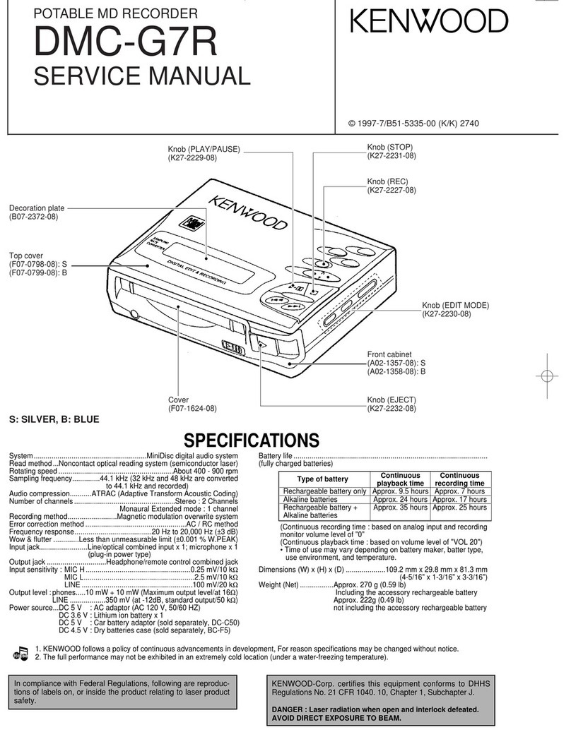
SPECIFICATIONS
PORTABLE MD PLAYER
DMC-K3
SERVICE MANUAL
© 1999-1/B51-5503-00 (K/K) 2837
In compliance with Federal Regulations, following are reproduc-
tions of labels on, or inside the product relating to laser product
safety.
KENWOOD-Corp. certifies this equipment conforms to DHHS
Regulations No. 21 CFR 1040. 10, Chapter 1, Subchapter J.
DANGER : Laser radiation when open and interlock defeated.
AVOID DIRECT EXPOSURE TO BEAM.
System ........................... Mini disc digital audio system
Read method ................. Noncontact optical reading system (semicon-
ductor laser)
Sampling frequency ...... 44.1 kHz
Audio compression ....... ATRAC (Adaptive Transform Acoustic Coding)
Number of channels ...... 2 channels
Frequency response ...... 20 Hz to 20,000 Hz (±3 dB)
Wow & flutter ................ Less than unmeasurable limit (±0.001 %
W.PEAK)
Input/Output terminal .. Remote control/Phones jack
Rated power output ...... 9 mW+9 mW
Power source
DC IN jack (4–5.1V)
: Specially provided AC adaptor
: Car battery adaptor (sold separately, DC-C70)
DC 1.5V : Commercially sold AA alkaline battery (LR-6) ×1
DC 1.2V : Specially provided rechargeable battery (NB-150) ×1
(Charging time : About 3 hours)
Battery life (Fully charge, with “PS on” setting ON)
Specially provided rechargeable battery (NB-150) ×1......... Approx. 7 hours
Commercially sold AA alkaline battery (LR-6) ×1 ............... Approx. 8 hours
÷ At 0.5mW+0.5mW output (32 Ωload ).
÷ Standard value during continuous use/charging in an temperature of
25˚C.
÷ Time of use may vary depending on battery maker, battery type, use
environment, and temperatute.
÷ Time will be shorter when “PS off” Mode is set.
Dimensions (not including protruding parts)
W :99 mm (3-7/8”)
H :17 mm (11/16”)
D :75 mm (2-15/16”)
Weight (Net)............ 115g (0.25 lb)
not including the accessory rechargeable batter
140g (0.31 lb)
including the accessory rechargeable battery
1. KENWOOD follows a policy of continuous advancements in development. For reason specifications may be changed without notice.
2.The full performance may not be exhibited in an extremely cold location (under a water-freezing temperature).
Notes
Notes
KENWOOD CORPORATION MADE IN JAPAN
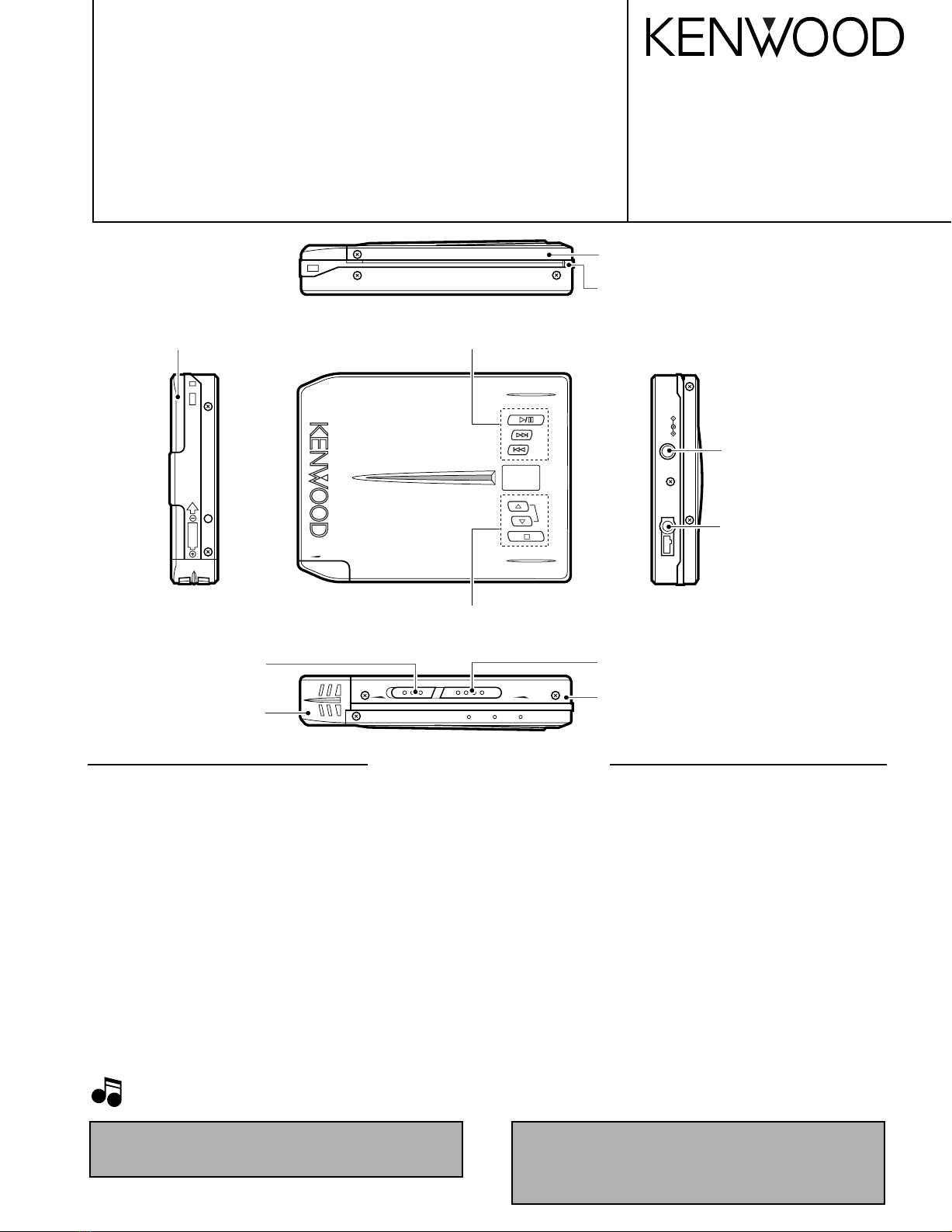
– VOLUME +
OPEN
DC IN 4 - 5. 1V
PHONES
BATTERY ( L6 .R6 .AA .AM3 ) 1 . 5V
NI - MH BATTERY 1 . 2V
IN
OPEN HOLD
Lid assy
(A53-2123-03)
Dressing panel
(A21-3741-04)
Knob
(K29-7476-03)
Knob
(K29-7478-04)
Knob
(K29-7477-04)
Battery cover
(A09-1118-03)
Miniature phone jack
(E11-0381-05)
Metallic cabinet assy
(A01-3664-03)
Escutcheon
(B07-2443-01)
DC jack
(E03-0357-05)
Knob
(K29-7475-03)
Illustration is DMC-K3(S).

DMC-K3
2
CONTENTS / ACCESSORIES
AC adapter (1) *
(W09-)
Remotcon (1)
(A70-1258-05) Stereo headphone (1) *
(W01-)
Stereo headphone (1) *
(W01-0963-05)
* Refer to parts list on page 17.
Batteries : NB150 (1)
(W09-1267-05) Carrying case (1)
(W01-0938-05)
Contents
Accessories
Caution
SPECIFICATIONS.........................................Top cover
CONTENTS / ACCESSORIES ....................................2
CONTROLS.................................................................3
DISASSEMBLY FOR REPAIR.....................................4
CIRCUIT DESCRIPTION.............................................5
PC BOARD ..................................................................9
SCHEMATIC DIAGRAM............................................11
EXPLODED VIEW .....................................................15
PARTS LIST...............................................................17
Action
÷Insert a MD into the unit.
÷Replace the disc with a
prerecorded MD when
playing it back.
÷Replace the MD.
÷Replace the MD.
Symptom Cause Remedy
÷The disc holder is not securely
closed.
÷The battery is depleted.
÷HOLD status is engaged.
÷The volume is at minimum
level.
÷The remote control or head-
phones are disconnected.
÷HOLD status is engaged.
÷The battery is depleted.
÷The remote control or head-
phone plug is not securely in-
serted.
÷The disc holder is not securely
closed.
÷The disc is scratched or dam-
aged or the recording is not
good.
÷The unit is in a place where
there is excessive vibration.
÷You are using commercial re-
chargeable battery.
÷The unit has become hot be-
cause of exposure to direct
sunlight etc.
÷You are using another AC
adaptor than the accessory
adaptor.
÷The AC adaptors has become
disconnected.
Unit fails to
turn ON.
÷Closedischoldersecurely.
÷Charge the battery.
÷Deactivate HOLD status.
÷Increase the volume.
÷Insert plug securely.
÷Deactivate HOLD status.
÷Charge the battery.
÷Insert plug securely.
÷Closedischoldersecurely.
÷Replace the MD.
÷Move the unit to a place
where there is little vibra-
tion or set to “PS off”.
÷Use the special recharge-
able battery (NB-150)
÷Wait until the unit has
cooledto normal tempera-
ture.
÷Use the accessory AC
adaptor.
÷Connect the AC adaptor
securely.
There is no
sound.
The unit does
not respond
to key opera-
tion.
Sound skips.
Troubleshooting
Message Meaning
÷There is no MD in the unit.
÷Nothing is recorded on this
MD.
÷The *UTOC contents are
faulty.
÷The disc is scratched or dam-
aged, so playback is not pos-
sible.
“BLANK ”
“noDISC”
“ERROR ”
Meaning of display messages
*UTOC: A recordable MD has an area for recording so-called UTOC
(User's Table of Contents) data. The UTOC contains number
of tracks, playing time, written data, and other rewritable
information.
Battery does
not charge.
Resetting the unit
This system uses a microcomputer so it may malfunction due to external
noise or interference. In such a case, unplug the power cord and remove the
batteries, then plug the power cord again and insert the batteries again.
Beware of condensation
When water vapor comes into contact with the surface of cold materi-
al, water drops are produced.
If condensation occurs, correct operation may not be possible, or the
unit may not function correctly.
This is not a malfunction, however, and the unit should be dried.
(To do this, turn the POWER switch ON and leave the unit as it is for
several hours.)
Be especially careful in the following conditions:
• When the unit is brought from a cold place to warm place, and there is
a large temperature difference.
• When a heater starts operating.
• When the unit is brought from an air-conditioned place to a place of
high temperature with high humidity.
• When there is a large difference between the internal temperature of
the unit and the ambient temperature, or in conditions where conden-
sation occurs easily.

DMC-K3
3
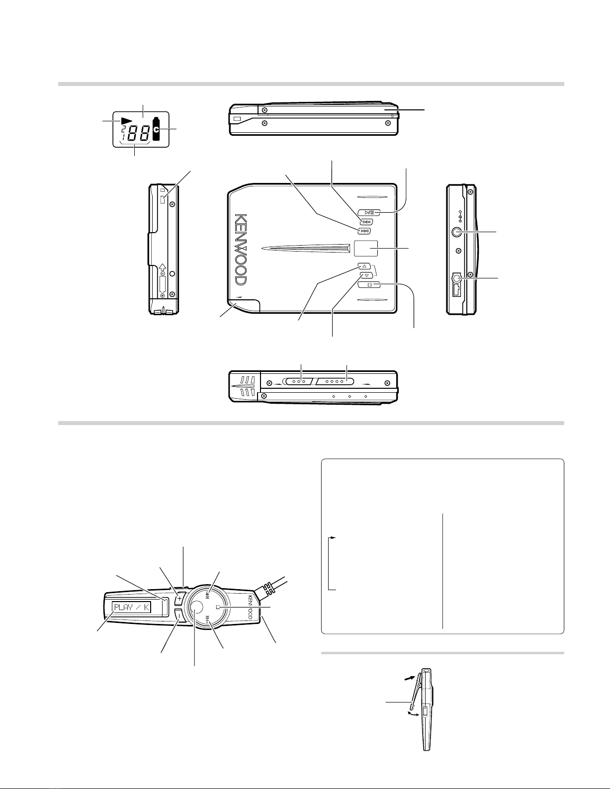
CONTROLS
KENWOOD CORPORATION MADE IN JAPAN
– VOLUME +
OPEN
DC IN 4 - 5. 1V
PHONES
BATTERY ( L6 .R6 .AA .AM3 ) 1 . 5V
NI - MH BATTERY 1 . 2V
IN
OPEN HOLD
M
O
D
E
^
HOLD
HOLD switch
6(Play/pause) key
5(Volume up) key
4(Skip down) key
HOLD indicator
Main Unit
Play indicator
Track number indicator
Battery
indicator
7(Stop/off) key
Charge key
LCD
DC IN jack
(Extemal power jack)
Battery cover
∞ (Volume down) key
OPEN slider
¢ (Skip up) key
PHONES jack
Disc Holder
HOLD
Using the Clip
÷ Clip the remote control unit to the
edge of your bag or pocket.
Remote Control
Clip
Press and release.
PHONES jack
Hand strap
attaching hole
¢ (Skip up) key
4(Skip down) key
MODE key
LCD
6(Play/pause) key
7(Stop/off) key
Charge key
HOLD switch
+ (Volume up) key
– (Volume down) key
The mode changes each time the
MODE key is pressed.
The mode changes each time the
MODE key is pressed.
MODE key
(Only by remote control operation)
1Fast forward/fast reverse
(search)
2Changing the display mode
3Play Mode
4Changing the tone
(BASS BOOST)
5Original display
1AUTO PLAY
2AUTO POWER SAVE
3Operating tone (Beep)
4Original display
Use this key to set playback-related features and other convenient
functions. Please also read “Playback (Application)” and “Convenient
functions” for details.
When the MODE key is held de-
pressed for more than 2 seconds:
÷ To change one of the above set-
ups after returning to the original
display, restart from the step of
pressing and holding the MODE
key for more than 2 seconds.

DMC-K3
4
DISASSEMBLY FOR REPAIR
1
1
1
1
2
1
1
1
3
3
7
3
3
65
4x2
x2
S1
How to Remove Case
1. Remove 7 screws(1).
2. Slide the case to the opposite side of the battery case(2).
How to Check PCB
3. Rmove 7 screws(3x5,4x2) and unsolder the corner of pcb(5).
4. Connect the ground wire to the LCD mounting hardware and the frame of the unit(6).
5. Fix the switch 1 (ON mode) by the tape(7). And check the unit with standing it.

5
DMC-K3
CIRCUIT DESCRIPTION
1. Main microprocessor : uPD784036GC831 (X33 : IC5)
1-1 Microprocessor periphery block diagram(X33)
1-2 Pin description
IC9
IC7
RE/SERVO
CXA2523AR DSP/ATRAC
CXD2655BR
SERIAL XLAT XRST FOK SQSY SENS
Q6
BEEP MIXER
IC5 Q17
XSTBY BEEP
BASS BOOST
BassBoost
IC12 SEIN MUTE SW IC8
u-COM HEAD PHONES AMP
MOTOR DRIVER S1-S3 uPD784036GC PSW LA4801V
BD6601KVT EPDO
EPDI IC10
BEMFU,V,W EPCS E2PROM
EPSK AK93C45AV
ED1 com
SEG1-19
LCD(SET)
SP PWS CHG1 CHG2 ADP CHGOK BATT
POWER SUPPLY CONTROL/RECHARGEABLE CIRCUIT
Pin No. Name I/O Description
Function H/L
1 XLAT O DSP IC (CXD2655BR) LATCH signal
2 XRST O DSP IC (CXD2655BR) HARD RESET signal
3 XSTBY O RF/SERVO IC (CXA2523AR) STAND BY signal
4 LDON O PICK UP LASER on/off signal L: LIGHTING H: NON LIGHTING
5 BEEP O BEEP output/ to HP AMP
6 BASS BOOST O Analog bass boost control L: BOOST ON H: BOOST OFF
7 RESET – µ-com RESET
8 VDD – µ-com +power supply
9 X2 O µ-com SYSTEM CLOCK OSC port (out)
10 X1 I µ-com SYSTEM CLOCK OSC port (in)
11 VSS – µ-com GND
12 LCD DATA O LCD remocon display data serial output
13 BEMFW I SLED MOTOR comparator signal(W)
14 BEMFV I SLED MOTOR comparator signal(V)
15 BEMFU I SLED MOTOR comparator signal(U)
16~18 S1~3 O SLED MOTOR control signal
for DRIVER input port
19 NC O –

CIRCUIT DESCRIPTION
DMC-K3
6
Pin No. Name I/O Description
Function H/L
SYSTEM POWER port
20 SP O DSP IC (CXD2655BR) H: ON
RF/SERVO IC (CXA2523AR) L: OFF
Motor Driver/HP amp VCC2 power supply
21 CHG1 O Rechargeable circuit control signal H: RECHARGEABLE
(SET UP POWER SUPPLY) L: NORMAL
22 CHG2 O Rechargeable circuit control signal H: RECHARGEABLE
(START RECHARGEABLE) L: NORMAL
TEST1/0
23,24 TEST0,1 I Test mode setting HH: TEST1
HL: TEST2/3
LH: TEST4
25~43 SEG19~1 O Set's LCD segment output 19~1
44 NC O –
45 VSS – µ-com GND
46 TEST – µ-com TEST port (CONNECT GND)
47 COM O Set's LCD COMMON
48 EPSK O E2PROM CLOCK output
49 PW SW O HP amp power supply H: ON
(CONNECT HP. AMP POWER SUPPLY PORT) L: OFF
50 MUTE SW O HP amp mute control L: MUTE ON H:MUTE OFF
51 PWS O DRAM/LCD remocon power supply port H: ON L:OFF
52 EPCS O E2PROM LATCH signal
53 EPDI O E2PROM DATA signal
54 EPDO I E2PROM DATA signal
55 VDD – µ-com +power supply
56 KEY0 I Set's key input TAKE IN A/D
57 KEY1 I LCD remocon key input TAKE IN A/D
58 ADP I Adaptor DC detector TAKE IN A/D
59 CHGOK I Rechargeable battery detector TAKE IN A/D
60 BATT I Battery DC input TAKE IN A/D
61 SEIN(REVERSE) I SLED ERROR signal (REVERSE) TAKE IN A/D
62 SEIN(FORWARD) I SLED ERROR signal (FORWARD) TAKE IN A/D
63 ADON O AVREF voltage output
64 AVDD – µ-com A/D power supply
65 AVREF1 – µ-com A/D reference voltage input
66 AVSS – µ-com A/D GND
67,68 NC O –
69,70 AVREF2,3 – µ-com D/A reference voltage input
71 JTYPE I – H: EXCEPT JAPAN L:JAPAN
72 HOLD I HOLD SW
73 XINT I DSP IC (CXD2655BR) H:
XINT EDGE intercept input L: óEDGE INTERCEPT
74 SQSY I DSP IC (CXD2655BR) H:
ADIP SYNC intercept input L: óEDGE INTERCEPT
75 LID SW I LID OPEN SW H: CLOSE L:OPEN
76 SCLK O DSP IC (CXD2655BR) SERIAL CLOCK input
77 W.UP I µ-com WAKU UP input H:
EDGE intercept L: óEDGE INTERCEPT
78 SENS I DSP IC (CXD2655BR) SENSE signal
79 SRDT I DSP IC (CXD2655BR) SERIAL DATA signal
80 SWDT O DSP IC (CXD2655BR) SERIAL DATA signal

DMC-K3
CIRCUIT DESCRIPTION
7
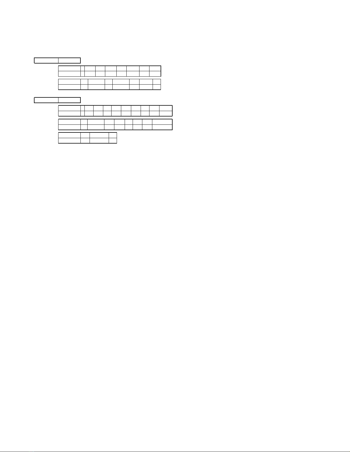
1-3 Voltage matrix key (u-COM pin ||,““)
2. TEST MODE
* Test mode I is required when disassemble or replace the
laser pickup and MD mechanism.
* Test mode I and II are required when replace the
E2PROM.
* Need the remote control for adjustment procedure.
How to Reset the Unit.
* Connect the AC adapter to the wall outlet with pressing
<SKIP> key.
* Contents of initialization.
Volume VOL 10
Repeat OFF
Bass boost BOOST 1
Remocon mode DISC/TRACK(title mode)
Auto Play OFF
Resume TNO TNO[1]
Auto power save ON
Beep ON
Display in Remocon [ENG]
Display in unit [En]
Power off after display shows for 2 seconds
2-1 TEST MODE I(Adjusting Mode)
* Contents(to memorize the adjustment result to E2PROM)
1) EF Balance(automatic/manual)
2) Focus Bias(automatic/manual)
Note:Automatic adjustment only in this manual
2-1-1 Setting
1) Connect the #24(P_TEST1) and 23(P_TEST0) ports
of IC5 to 2.8v(VDD) port. Next to AC adapter.
Mode is STOP.
Remote cont [TEST1]
Unit [o1]
2) Press the SKIP UP key. To memorized the proper
value of FE balance automatically. Manual adjust-
ment if press the SKIP DOWN key.
2-1-2 Automatic FE Balance and FOCUS Bias
Adjustment
1) The FE balance setting value of the default starts a
servo by the value which is memorized in E2PROM.
Incidentally, there are 3 kinds of memory
area(high/Low reflection Pit/Low reflection
groove)which store a balance setting value E2PROM.
At the time of automatic adjustment this 3kinds of
areas are used appropriately according to a disc.
* There is a setting range of 32 steps(00h-1Fh) in the
balance setting value. The default value are
High reflection 51h
Low reflection 10h (pit)
Low reflection 90h (groove)
2) Display shows the following if automatic adjustment
proceeds.
Remote cont [WAIT O] --- O means in operation
mode.
Unit [o1]
3) Adjustment is over if loading the pre recorded disc. In
case of the recordable disc, the servo will be "03"
mode. Read the TOC in lead area and read the head-
er and access lead -in area in CPLAY mode
Remote cont [WAIT O]
Unit [o1]
4) Proceed pit area adjustment after TOC read if loading
the recordable disc. Change to focus bias check after
TOC read if loading the pre recorded disc.
Remote cont [WAIT O]
5) Change to FOCUS Bias step after pit area adjustment
if loading the recordable disc.
Remote cont [WAIT O]
Unit [o1]
2-1-3 Focus Bias Check
1) The Focus bias will be adjusted automatically at the
focus bias points(+16,0,-16)
Remote cont [*80 OO] left 2 figures:
bias setting value +80h right 3 figures: C1 error
rate(OVR;4 figures)
2) Display shows setting value+80h. Press the
PLAY/PAUSE key to stop Automatic Adjustment.
Remote cont [*80 10] changed value
[TEST 1] the play/pause
key is pressed
Unit [o1 changed value
[oo] the play/pause
key is pressed
2-2 TEST MODE II (AUDIO SPEC)
* Item of audio specification(use test disc TDYS1)
1) Reference
TNO[ 2]: 1kHz sinewave,0dB,L &R, Emphasis off
0Port voltage [V]
SET 6KEY PIN 56 KEY0
67
67
4¢
4¢
0.4
Key function
Port voltage [V]
Key function
Port voltage [V]
REMOCON 8KEY PIN 57 KEY1
Key function
Port voltage [V]
Key function
Port voltage [V]
Key function Non remocon
0.8 1.2
0 0.21 0.46 0.73 1.02
1.6 2 2.4 2.8
VOL.DOWN VOL.UP KEY OFF
VOL.UP
1 1.6 1.9 2.23
VOL.DOWN MODE HOLD Exist remocon
2.57 2.8

CIRCUIT DESCRIPTION
DMC-K3
8
2) Frequency Response
TON[ 3]: 40Hz sinewave,0dB,L&R,Emphasis off
3) Modulation Noise
TON[ 6]: 20kHz sinewave,0dB,L&R,Emphasis off
4) Noise Ratio
TON[ 7]: 40Hz Infinity Zero,- dB,L&R,Emphasis off
5) Channel Separation
TON[ 8]: 1kHz sinewave,0dB,L,Emphasis off
6) Channel Separation
TON[ 10]: 1kHz sinewave,0dB,R,Emphasis off
7) Deemphasis
TON[ 13]: 16kHz sinewave,-9.04dB,L&R,Emphasis
on
2-2-1 Procedures
1) Connect #23(P_TEST0) of IC5 to 2.8V(VDD) and
#24(P_TEST1) of that to GND. Next Connect AC
adapter to the unit.(the unit will be in CPLAY mode
after TOC reads)
Remocon [TEST 4]
Unit [o4]
2) The unit will be in CPLAY after TOC reading.
Remocon [TOC OK]
Unit [o4]
3) Choose and playback TNO-02 on the disc by
PLAY/PAUSE key
Remocon [02] playback TNO
Unit [o4]
4) Choose and playback every TNO in the above table
by PLAY/PAUSE key. TNO will be chosen TNO 02 if
repressing the PLAY/PAUSE key after STOP key
pressed,
Remocon [03] playback TNO
Unit [o4]

ACEGIBDFHJ
2
1
3
5
7
4
6
Refer to the schematic diagram for the value of resistors and capacitors.
PC BOARD(Component side view)PC BOARD(Foil side view)
9 10
S2
IC7
IC5
IC8
IC12
IC10
Q14
Q6
D5
D1
Q13
IC13
D10
Q9
S8
S7
S4
S5 S6
S3
CN2
STOP
VOLUME VOLUME PLAY
CN1
ED1
IC9
C36
R52
C32
L6
R30
R49
R31
R62
C66
C25
C30
L5
C67
C47
C57
C7
X2
X1
C53 C34
C41
C23
C56
R48
R55
C29
C54
C31
R54
R53
R1
L4
C37
C35
R65
C65
C50 R46
R41
R43
C39
C40
R42
R40
C27
R67
R27
R108
R109
R45
R15
C111
C110
R58
R47 R63
C24
R100
R101
R111
R110
C38
C12
R72
R38
R21
R29
R36
R28 C62 C21
C20 C19
C9
R17
R66
R24
R25 R26
R35
R34
C43
C44
C15
C14
C11
L2
C63
C33
C52
C42
C45
C49
C26
C5
C46
R13
C64
C59
C58
C61
R39
C16
R51
C28
C51
51
34
1
8
18
54
21 40
80 61 60
41
1
20
76 100
50 26 25
1
75
51
112
13
24 37
48
36
25
1
22
1
10
20
11 1
20
21
40
41
60
61 80
20 1
TE
FE RF
FCONT
MNT1
2
3
VDD
TEST0
TEST1
DO
DI
SK CS
CHGOK
BATT
FVC
EB
E
B
EB
EB
L3
L1
R71
R57
R44
R73
C115
C8
R37
R9
C55
R8
R74
C1
R11
R19
R10
C102
C103
C106
C112
R50
R103
R112
R113 C114
R106
C109
R6
C108
C48
R107
C113
C101
C60
C119
C116
C105
R105
C104 R104
R102
R59 R32
R33
C22
C17
C18
R14 R22
R70
C68
C3
C4
C6
R12
R23
R20
R18
R16
R7
R2
C10
C2
R56
R5
R69
R4
R64
R3
R60
C13
C100
D
G
D
G
EB
BE
B
E
EB
EB
EB
EB EB
E
B
E
B
8
1
16 9
S
G
I
O
S
E
B
CB
E
C
54
31
13
45
V
C
W
C
U
Y
WU
SP
SL
18
17
19
16
14 12
15 10
11
9
8
5
13
67
3
4
2
1
COM
ADP
S3
VDD
TEST0
TEST1
RESET
FOK
FGIN
SL+
ABCD
SL-
S1
S2
I
C
F
ILCC FCS-
TRK+
TRK-
FCS+
A
JE
VC
RF0
B
D
VCC
PD
VEE
ADIN
CHG
1
3
4
2
IC6 Q15
D12
Q1
Q2
Q12
D8
Q17
D6
Q16
D11
D4
Q10
D7
Q3
D2
IC1
IC2
Q4
IC4
Q5
IC3
Q7
D3
D9
Q11
Q8
S1
J1
PHONES DC IN
(J70-1290-02)
X33-1180-00
OPEN
J2
IC5
D10
Q13
Q14
S2
CN1
IC13
IC8
IC12
Q9
IC9
Q6
IC7
IC10
PLAY
STOP
ED1
VOLUME
S4
S7
VOLUME
S8
S5
S3
S6
D1
D5
CN2
C27
X2
R29
R36
BE
80 C40
VC
R42
C38 BE
BE
R40
C39
R43
R46
R41
C51
F
22
C41
1
51
50
C67
C49
20
R62
1
34
R31
R49
C59
41
C64
C58
15
R30
40
C32
10
26
C26
11
25
C15
C14
C11
L5
60
C45
L6
R28
C62
61
C65
R67
C36
24
R27
R1
12 C50
13
25
C37
R48
TE
C56
C23
C30
C34
C33
48
C52
37
C53
1
R52
C57
R53
R54
C28
R55
R51
C110
R66 FE
R65
RF
C29
36
C35
C54
C31
76
75
R111
R110
EB
L4
R17 R13 R34
R35
R100
C111
FCONT
R101
R45
C25 C24
R47
31
2
MNT1 100
R72
C12
C61
R63
1
R58
X1
20 R21 C5
20
VDD R15
R38
TEST1
21
TEST0
61
C63
20 21
C42
C43
C44
C7
C21
80
C66
1
C9
L2
BATT
60
CHGOK C20
41
C19
1
40
4
SK
DI
DOCS
8
5
C47
R24
R26
R25
R109
R108 R39
C16
C46
1
81
E
C60
R102
C4C55
10
B
FCS+
TRK-
VCC
D
F
ILCC
FCS-
TRK+
A
E
C
VC
I
J
PD
VEE
SL-
S1
S2
ABCD
R73 BE
R103
C102
C103
C106
R112
ADIN
RF0
R44
R107
GD
S
R106
R9
C101
C104
1
C116
C114 R113
8
C113
C115
C100
916
R105
C119
C105
R104
C112
R50
FOK FGIN
R37
C68
ER3
SL+
B
2
4
3
14
5
S3
TEST1
R64
RESET
TEST0
16
513
6
C2
R5
R11
R6
I
13
R4
R56
1
BE
O
D
G
S
BE
EB
G
B
R2
5C10
B
VDD R74
R69
3
BE
15
12 14
19
17
18
B
CE
C1
4
E
R7
E
B
R18
R23
R12
R16
R20
R14
R70
C18
C17
C22
R59
CHG
R10
R19
9
R33
R22
R32
C8
COM
ADP
1
7
8
2
311
4
W
R60
C48
EB
C13
C108
C109
L3
C3
L1
R8
C6
C
B
E
R71
R57
SP
UWSL
U
C
Y
C
V
Q3
D8
Q17
S1
OPEN
Q15 IC6
D6
Q7
IC4
IC1
IC3
Q5
Q4
Q12
IC2
Q11
D9
Q2
D7 D4
Q16
D12
X33-1180-00
(J70-1290-02)
J1
PHONES
J2
Q1
D3
D2
Q10
D11
Q8
DC IN

ABDFHJCEGI
2
1
3
5
7
4
6
1
2
3
4
5
6
7
8
1
2
3
4
5
6
7
8
9
10
DQ1
DQ2
WE
RAS
A9
A0
A1
A2
A3
VCC
20
19
18
17
16
15
14
13
12
11
GND
DQ4
DQ3
CAS
OE
A8
A7
A6
A5
A4
3
4NC
VSS
2
1
VDD
OUT
80
79
78
77
76
75
74
73
72
71
70
69
68
67
66
65
64
63
62
61
60
59
58
57
56
55
54
53
52
51
50
49
48
47
46
45
44
43
42
41
21
22
23
24
25
26
27
28
29
30
31
32
33
34
35
36
37
38
39
40
1
2
3
4
5
6
7
8
9
10
11
12
13
14
15
16
17
18
19
20
PW2VM
PW2OUT
N.C
PWPG
N.C
PW1OUT
N.C
PW1VM
N.C
SLPG2
SLWOUT
SLVM2
N.C
SLVOUT
N.C
SLPG1
SLUOUT
N.C
SLVM1
SLCOM
BEMFW
BEMFV
BEMFU
S3
S2
S1
STHB
STALL
VG
C2M
C2P
C1M
C1P
EXTCLK
IN2R
IN2F
IN1R
IN1F
VCC2
VCC1
SPCOM
SPWIN
SPVIN
SPUIN
H2PG2
N.C
H2ROUT
N.C
H2VM
N.C
H2FOUT
N.C
H2PG1
H1PG2
N.C
H1ROUT
N.C
H1VM
H1FOUT
H1PG1
SGGND
ASGND
PWIN1
PWIN2
FG
BRK-
BRK+
CSL2
CSL1
CST
SPPG2
SPWOUT
SPVM2
N.C
SPVOUT
N.C
SPPG1
N.C
SPUOUT
SPVM1
30
29
28
27
26
25
24
23
22
21
21
22
18
20 SP
CHG1
S3
19
S2
S1
17
16 BEMFU
BEMFV
15
14
TEST0
CHG2
SEG19
TEST1
SEG16
SEG17
SEG18
SEG14
SEG15
VSS
BEMFW
LCD DATA
13
12
X1
11
10
X1
16MHz X2
9VDD
RESET
8
SWDT
3
5
B.B
BEEP
7
6
LDON
XSTBY
4
XRST
XLAT
2
1
80
75
SCLK
W. UP
SENS
SRDT 78
79
76
77
HOLD
XINT
SQSY
LID SW
72
73
74
80
R45
78
79
10K
76
73
74
86
88
62
94
COMMAND I-F
CPU
3T DETECTOR
OPAMP
USER
17
C50
0.01
2.2Kx4
R46
C51
0.01
82
R42
4.3
C39
22u4
C38
1000P
+
14
13
16
15
GND
12
11
10
AMP
TEMP
APC
9
8
7
6
FE AMP
I-V AMP
VC
4
5
3
2
AMP
ABCD
1RF AMP
47
48
45
46 0.022
C53
C33
0.1
100P
470K
54
SEQUENCER
ANALOG MUX
CONVERTER
76
78
81
80
79
78
77
82
81
80
C54
0.1
75
74 AUTO
A/D
73
72 AVSS
71
70 AVDD
+
80
81
R27 13K
R1 13K
C23
22u4
19
18
21
20
VREF
F0CNT
XSTBY
24
23
22
R44
56K
VCC
3TADJ
EQADJ TE/SE
AMP
WBLADJ 25
26
27
28
0.1
4700P
C37
66
65
64
63
62
68
69
67
66
65
64
63
62
C29
4700P
R52
33K R53
1M
PLL
61
60
59
56
58
57
AVSS
55
DECODER
EFM/ACIRC
8
GENERATOR
93
83
82
85
84
83
87
86
85
89
61
90
89
88
92
91
DVDD
99
93
96
95
94
98
97
100
TEST3
TEST2
TEST1
DVSS
1
SERVO
PWM
DSP
DECODER
ADIP
CONTROL
MONITOR
SERVO
SPINDLE BLOCK 2
3
4
5
BLOCK
6
I/F
CPU 7
100Kx4
R58
76
80 73
1
79
TST2
PROCESSOR
SUBCODE
9
10
11
S12
13
DAVDD 14
15
LPF OSC
CELL 16
17
DAC DAVSS 18
19
TST1 20
21
2
78
74 C24
0.01
R63 27
X2
22.579MHz
R47
330
MUX
ADIPAMP
29
30
31
32
BOTTOM DETECTOR
PEAK,
35
33
34
36
C36
1
C35
66
64
65
63
EQ
AGC,
COMP
USER
42
43
44
40
41
37
38
39
0.01
C52
C34
0.22
62
C27
0.47
C28
R54
100K
R55
53 AVDD
52
51
COMP 4
50
47
48
49
44
45
46 47
48
49
44
45
46
MEMORY CONTROLLER
SHOCK RESISTANT
12
24
DIGITAL
AUDIO I/F 22
NC 23
ATRAC
DVDD
25
41
42
43
38
39
40
35
36
37
32
33
34
41
42
43
38
36
35
37
32
34
29
30
31
27
28
26
29
31
30
+
C26
22u4
X33-1180-00
UNIT No.
DESTINATION
JAPAN
COUNTRY J
ABB. YES NO
R29
9
17
I
J
C
F
VEE
21
22
20
19
18
LDGND
VCC
VC
B
D
A
E
NC
13
16
15
14
12
11
10
VR
FCS-
TRK+
TRK-
FCS+
PD-K
ILCC
NC
PD
8
7
6
5
4
3
2
1
WU
V
COM
COM
V
UW
39
36
31
27
1
2
9
8
1
2
8
9
3
3
680
R41
0.022
C40
470K
R40
R48
100Kx2
6800P
+
C25 47u4
94
93
95
90
R19 100K
R10 150K
C42 0.033
C43 0.033
C44 0.22
15
12
19
2200P
15K
R59
C22
C18
C17
2200P
2200P
16
17
13
18
14
15
C11 0.1
C14 0.1
C15 0.1
C49 0.1
88
89
85
86
70
67
64
61
47u4
+
L5 22uH C67
47 49
48
46
42
45
41
44
38
43
37
32
36
31
35
30
34
29
33K
R3
10K
R4
330
R5
10u10
+
4
5
1
2
3VO
VDD
GND
EXT
CE
3
4
5
6
C12 0.01
R64 10K
2.7K
R38
17
18
13
16
15
14
100Kx2
R15
S19
S18
S17
S16
S15
S14
2
1
C61
470K
R72 1K
R13
67
70
61
64
15
19
12
21
22u4
C41
+
83 L4 22uH
10K
R17
0.033
C65
79
100K
R43
3
78
73
74
0.033
C57
10K
R51
0.1
C31 0.22
C30
73
74
79
90
95
4
L2
+
47u4
C63
2
21
100Kx2
R9
13K
R21
20
2
B
+B
Q9
20
R28
+
22u4
0.1
C45
C68
150K
R11
4
12
27
36
31
39
+B
+B+B+B
+B
+B+B+B
+2.8V
+2.8V+2.8V
+2.8V
+2.8V
+2.8V
+2.8V+2.8V
+2.8V
+2.8V+2.8V
+2.8V +2.8V
+2.8V
+2.5V +2.5V
+2.5V+2.5V+2.5V
+2.5V+2.5V
+2.5V
+2.5V
+2.5V+2.5V
+2.5V
+2.5V+2.5V
+2.5V +2.5V
+2.5V
+2.5V
+2.5V
+2.5V
+2.5V
+2.5V+2.5V
+2.5V+2.5V+2.5V
+2.5V +2.5V
+2.5V
+2.5V+2.5V+2.5V+2.5V
+2.5V
+2.5V
+2.5V
+2.5V
+2.5V
+2.5V
+2.8V
+2.5V
C32
1
+2.8V
+2.5V
+2.8V
VC
VCC
GND
C56
NC
22uH
C5
100u4
+
X33-1182-71
X33-1180-00
UNIT No.
U.K.
JAPAN
COUNTRY
EUROPE E
T
ABB.
J
DESTINATION R29R28
NO YES
YES NO
X33-1182-71
UNIT No.
U.K.
U.S.A.
COUNTRY
EUROPE E
T
ABB.
K
DESTINATION R29R28
NO YES
SPCOM
SPW
SPU
SPV
SLU
SLCOM
SLW
SLV
IC4
u-COM
MOTOR
SLED
MOTOR
SPINDLE
APC
Q14
CN1
B
A
JI
C
E
D
F
CN2
Q5
Q7
S1
Q9
LID SW
Q13
D10
D8
IC5
WAKE UP
FOCUS COIL
TRACKING COIL SERVO
RF AMP
APC
ON/OFF
P.U. VCC
SHOCK PROOF
4M DRAM
GND LINE
SIGNAL LINE
B LINE
B LINE
DAC
DSP
DRIVER
MOTOR 2.5V AVR
ON/OFF
2.5V
REGULA-
TOR
IC
RESET
DIGITAL
ANALOG(R)
ANALOG(L)
IC1 : XC6365B103MR
IC2 : XC6383B281MR
IC3 : XC62EP2502MR
IC4 : S-80823ALNP
IC5 : UPD784036GC831
IC6 : LA4801V
IC7 : CXD2655BR
IC8 : MN41V4400TT-07 or
MN41V4400TT-08
IC9 : CXA2523AR
IC10 : AK93C45AV
IC12 : BD6601AKVT
IC13 : NJU7011F
Q1,11,15 : CPH3106
Q2 : DTC323TK
Q3 : XP161A0390PR
Q4,6,9 : DTC114YUA
Q5,14 : 2SA1745(6.7)
Q7 : 2SC4116(Y,GR)
Q8 : CPH3209
Q10 : UMX1N
Q12,16 : DTC114TUA
Q13 : DTA114EUA
Q17 : 2SK3018
D1,7,10,11 : MA111
D2,3,5 : U2FWJ44N
D4 : RB717F
D8,12 : DA204U
D9 : UDZ10B
(BOTTOM VIEW)
(BOTTOM
VIEW)
B38-0172-05ED1 :
DMC-K3(L)
DMC-K3(S)
DMC-K3(BL)
IC8
IC4
IC12
IC5
(X33-1180-00)
IC9
IC7
MECHA. ASS'Y MDP-03 (X92-2140-10)
PICKUP (KMS-281A)
IC3
2.8V
0V
1.7V
0V
0.7V
0.6V
2.8V
0V
0V
2.7V
2.8V
2.8V
0.3V
2.0V
2.5V
2.7V
2.3V
2.5V
2.6V
2.5V
0V
1.2V
1.2V
1.1V
1.3V
1.1V
1.1V
1.4V
1.3V
1.3V
1.3V
1.3V
0.6V
0.3V
1.2V
2.6V
2.6V
2.6V
1.4V
1.3V
2.6V
0V
0.4V
1.2V
2.8V
0V
1.3V
0.6V
1.3V
2.6V
1.3V
1.4V
1.2V
1.4V
1.3V
1.9V
1.4V
1.2V
1.4V
1.2V
1.3V
2.0V
2.8V
2.5V
2.8V
0V
0V
2.6V
0V
0V
0V
2.6V
2.7V
0V
1.1V
1.2V
1.1V
1.1V
1.3V
1.2V
0.8V
1.2V
1.4V
1.4V
1.3V
1.4V
1.3V
1.6V
1.7V
1.7V
1.9V
1.3V
2.6V 1.3V
2.5V
2.5V
2.5V
2.5V
2.6V
2.5V
2.5V
2.5V
0V
1.1V
2.5V
1.0V
2.5V
1.2V
2.5V
2.5V
2.5V
2.5V
2.6V
2.5V
2.6V
2.6V
0V
0V
0V
0V
0V
0V
2.5V
2.6V
2.5V
2.8V
2.5V
2.5V 1.0V
1.2V
0V 1.1V
2.5V
2.6V
2.5V
2.5V 2.5V
2.5V
2.5V
2.5V
2.5V
2.5V
2.5V
0V
2.5V
2.8V
2.6V
2.6V
2.5V
1.9V
2.6V
2.6V
0V
0.3V
2.8V
0V
0.2V
0V
0.3V
2.2V
2.1V
1.0V
2.6V
1.5V
1.3V
0.6V
0V
0V
0V
0V
0V
0V
0V
0V
2.6V
0V
0V
0V
0V
3.7V
1.3V
6.2V
1.3V
7.4V
2.7V
2.6V
2.8V
0V
2.8V
1.8V
0V
0V
1.4V
1.4V
1.4V
1.4V
1.8V
1.8V
1.8V
1.8V
0.3V
2.8V
2.8V
2.8V
2.8V
1.3V
1.1V
2.8V
2.8V
2.8V
1.4V
2.8V
0V
2.5V
2.8V
2.55V
2.2V
2.0V
2.6V
2.8V
2.5V
2.1V
2.8V
2.8V

KMOQSLNPRT
DMC-K3
Y22-8020-00
CAUTION: For continued safety, replace safety critical com-
ponents only with manufacturer's recommended parts (refer
to parts list). indicates safety critical components. For
continued protection against risk of fire, replace only with
same type and rating fuse(s). To reduce the risk of electric
shock, leakage-current or resistance measurements shall
be carried out (exposed parts are acceptably insulated from
the supply circuit) before the appliance is returned to the
customer.
The DC voltage is an actual reading measured with a high
impedance type voltmeter. The measurement value may
vary depending on the measuring instruments used or on
the product.
HOLD
C
1
2
3
4
5
6
7
8
16
15
14
13
12
11
10
9
EPSK
32
31 SEG13
40
39
38
37
36
35
34
33
SEG10
SEG11
SEG12
SEG7
SEG8
SEG9
SEG4
SEG5
SEG6
SEG3
SEG2
SEG1
TEST
NC
VSS
COM
DO
SK
CS
41
42
43
GND
VDD
ND
5
6
7ND
8
44
45
46
47
DI
4
3
2
1
70
NO J TYPE 71
PW SW
MUTE SW
PWS
EPCS
EPDI
EPDO
VDD
KEY0
52
50
48
49
51
54
53
55
56
CHGOK
KEY1
ADP
AVREF1
AVSS
NC
NC
AVREF2
AVREF3
67
68
69
64
65
66
BATT
SE-
SE+
ADON
AVDD
61
62
63
57
0.01
58
C20
22K
R32
59
C8 0.01
60 C9 1
R14
33K
+
22u4
C21
PW SW MT SW
300K
PW A
3K
PW C
PW B
3K
BIAS
VREF
FILTER
RIPPLE KEY
VDD
GND
VC
Lch
Rch
DATA
+
4.7u4
C113
+
4.7u4
C114
0.01
C109
2.2
R109
R108
2.2
0.01
C108
0.15
C104
4.3
R104C105
0.15 R105
4.3
+
4.7u4
C119
1
C101
1
R102 1
C100
R60
100Kx2
1
C60
47u4
C115
+
10K
R100
3.3M
R110
+
4.7u4
C110
6.2K
R106
1500P
C102
560
R112
C106 0.1
100K
R103
10K
R101 C111
4.7u4
+
R113
560
R111
3.3M
R107
6.2K
C103
1500P
R73
13K
C13 0.01
C16 0.01
750
R39
1000P
C46
C48
0.01
L3 22uH
VOUT
EXTVSS
12
3
4.3K
R6
C55 100u4
+
C4 100u4
+
560
R12
1.2K
R23
3.9K
R18
240
R20
0.33
R8
2.7K
R16
C3 100u4
+
R2 3.3K
470P
C2
330
R56
1/4W
C10 0.01
L1 22uH
8.2K
R7
10K
R74
1K
R69
0.1
C6
6.8K
R57
56K
R71
3
2
15
4GND
VIN
EXT
CE
FB
S13
S12
S11
S10
S9
S8
S5
S6
S7
S4
COM
S1
S2
S3
R22 150K
100Kx2
R62
HOLD ON
330K
R36
R29 470K
470K
R28
C62 0.1
R37
100Kx2
C66 1
C7 1
61
62
10K
58
59
C19
0.01
10K
R33
51
C58
0.01
R30
560Kx4
180Kx2
R31
130K
R49 0.01
C59
0.01
C64
45
2
1
3
6
50
49
Q8,10
Q1,3,12
IC2
Q17
2.7K
R24 R25
3.0K R26
4.3K R34
8.2K R35
18K
59
60
L6
22uH
4.7u4
C112
+
22u4
C116
+
2.2
R50
51
R70
58
5
12
57
57
0.01
C47
16
16
50
49
60
+B
+B
+B
+B
+B +B
+B+B
+B +B +B
+B +B
+B +B
+B
+B
+B
+B
+2.8V
+2.8V
+2.8V +2.8V +2.8V
+2.8V +2.8V
+2.8V
+2.8V +2.8V
+2.8V
+2.8V
+2.8V
+2.8V +2.8V
+2.8V +2.8V
+2.8V
+2.8V+2.8V
+2.8V +2.8V
+2.8V +2.8V
+2.8V
+2.8V
+2.8V
+2.8V
+2.5V
+2.5V +2.5V
+2.5V +2.5V
+2.5V
+B
21
22
20
19
18
17
16
15
14
13
12
11
10
9
8
7
6
5
4
3
2
1
SEG19
SEG18
SEG17
SEG16
SEG15
SEG14
SEG13
SEG12
SEG11
SEG10
SEG9
SEG8
SEG7
SEG6
SEG5
SEG4
SEG3
SEG2
SEG1
COM
S19
S18
S17
S16
S15
S14
S13
S12
S11
S10
S9
S8
S7
S6
S5
S4
S3
S2
S1
COM
2
10K1K10K
22u16
C1
+
E PROM
VOL
J1
Q16
Q6
Q17
D12
GND
J2
SW
+B
CAR BATTERY
AC ADAPTOR
Q11
Q1
Q2
IC2
Q12
Q3
Q15
Q4
Q8
Q10
D11
D3
D2
D9
D5
D1
D4
D7
S2
HOLD SW
IC13
DC IN 4.0-5.1V
ALKALINE BATT. : 1.5V
Ni-HM : 1.2V
(STEP DOWN)
DC-DC
CONVERTER
PROTECTION
CONTROL
RECHARGEABLE
CURRENT
SWITCHING TR
(STEP UP)
CONVERTER
DC-DC
ON/OFF
2.8V
AMP
MUTE
AC ADPTER
SOUND
BEEP
BOOST
BASS
PHONES AMP
PHONES
VOL
S3 S4 S5 S6 S7 S8
J
K : 4.5V/450mA
: 5.1V/380mA
: 4.0V
(BOTTOM VIEW)
ANALOG(R)
ANALOG(L)
ANODE CONNECTION
COM1
PIN
S12 1a3 1b4 1c5 1d6 1e7 1g8 1f9 S210 2a11 2b12 2c13 2d14 2e15 2g16 2f17 S318 S419 S520
COM
: 4.5V/600mAE,T
IC1
ON/OFF
IC6
IC10
(X33-1180-00)
IC1
ED1
DMC-K3(S)/(L)/(BL)
2.8V
0V
0V
0V
0V
0V
0V
0V
2.8V
2.8V
2.8V
2.8V
1.9V
edc
g
fb
a
dce
fgb
a
S3
S4
S5
21
S2 S1
1.4V
1.4V
1.4V
1.4V
0V
2.8V
2.8V
2.8V
0V
2.8V
2.8V
0V
2.2V
0.8V
1.6V
0.8V
0.8V
0.8V
2.1V
1.4V
0.7V
0.7V
0.7V
2.2V
2.1V
2.1V
0V
0.8V
2.8V
0V 1.0V
0V
2.8V
(1.7V)
(1.3V)
1.0V
1.4V
2.8V 2.8V
2.2V
(0V)
0.8V
0V
0V
0V
(1.2V)
1.0V
6.6V
(0.9V)
(1.3V)
(0.8V)
5.5V 6.7V
(0.9V)
(0.8V)
6.3V
6.3V
(0V)
6.7V
(0.9V)
(1.3V)
1.0V
(1.2V)
0V
2.0V
(0.4V)
2.8V
0V 0.7V
0.8V
( ) : BATTERY USE
DTC114YUA
DTC323TK
2SA1745
2SC4116
AK93C45AV
DA204U CXA2523AR
CXD2655BR
DTA114EUA

15
DMC-K3
EXPLODED VIEW (MECHANISM)
DMC-K3 MECHA
A ø1.7x3
B ø1.7x1.8(BLK)
C ø1.4x3 (BLK)
D ø1.4x3 (BLK)
E WASHER
: N09-3279-05
: N09-3104-05
: N09-3488-05
: N19-3369-05
: N19-1416-04
A
A
B
C
D
Cx2
801
E
Dx3
20
13 11
9
14
7
8
1
17
10
16
15
FM
DM
23x2
PU
1
2
3
AB
Parts with exploded view numbers larger than 700 are not supplied.

16
DMC-K3
EXPLODED VIEW (UNIT)
Parts with exploded view numbers larger than 700 are not supplied.
DMC-K3
A M1.4x2
B M1.4x1.5
C ø1.6x3(BLK)
D WASHER
: N09-3486-05
: N09-3487-05
: N78-1730-45
: N19-1416-04
S 2
S 3
S 6
S 5
S 8
S 7
S 4
S 1
J 1
J 2 ED1
661
662
660
608
663
771
737
742
738
748 713
770
745
744
640
636
635
620
640 621
628
625 603
651
653
652
650 641
626
602
640
747
712
730
701
731
646
645
627
629
611
606 610
607
A
A
A
A
D
Bx2 Bx2
C
C
Bx5
A
A
A
A
A
A
VOLUME
OPEN
HOLD
PHONES
VOLUME
DC IN
664
(K type)
(NB-150)
1
2
3
CD

DMC-K3
17
PARTS LIST
602 3D ✽A01-3662-03 METALLIC CABINET ASSY K1
602 3D ✽A01-3664-03 METALLIC CABINET ASSY E1T1
602 3D ✽A01-3670-03 METALLIC CABINET ASSY E2T2
603 3C ✽A09-1118-03 BATTERY COVER E1T1
603 3C ✽A09-1119-03 BATTERY COVER K1E2T2
606 1D ✽A21-3741-04 DRESSING PANEL E1T1
606 1D ✽A21-3750-04 DRESSING PANEL K1E2T2
607 1D ✽A53-2123-03 LID ASSY E1T1
607 1D ✽A53-2125-03 LID ASSY K1E2T2
608 1C ✽A70-1258-05 REMOTE CONTROLLER ASSY
610 1D ✽B07-2442-02 ESCUTCHEON ASSY E1T1
610 1D ✽B07-2444-02 ESCUTCHEON ASSY K1E2T2
611 2D ✽B07-2443-01 ESCUTCHEON
- B46-0100-50 WARRANTY CARD E1T1E2
- B46-0100-50 WARRANTY CARD T2
- B46-0197-00 QUESTIONNAIRE CARD K1
- B46-0328-03 WARRANTY CARD K1
-✽B60-4092-00 INSTRUCTION MANUAL(EN) T1K1T2
-✽B60-4093-00 INSTRUCTION MANUAL(FR) E1E2
-✽B60-4094-00 INSTRUCTION MANUAL(GE) E1E2
-✽B60-4095-00 INSTRUCTION MANUAL(NE) E1E2
-✽B60-4096-00 INSTRUCTION MANUAL(IT) E1E2
-✽B60-4097-00 INSTRUCTION MANUAL(ES) E1E2
620 2C ✽D10-3847-02 ARM ASSY
621 2C ✽D21-1930-04 SHAFT
625 3C ✽E23-1776-04 TERMINAL ASSY
626 2D ✽E23-1780-04 TERMINAL
627 2D ✽E23-1781-04 TERMINAL
628 3C ✽E23-1779-04 TERMINAL
629 2D ✽E29-1642-05 CONDUCTIVE RUBBER
635 2C ✽G01-4103-04 EXTENSION SPRING
636 2C ✽G01-4104-04 EXTENSION SPRING
- H21-0347-04 PROTECTION SHEET
- H25-0336-04 PROTECTION BAG
- H25-1588-04 PROTECTION BAG (BATTERY)
-✽H50-3198-03 ITEM CARTON CASE K1
-✽H50-3199-03 ITEM CARTON CASE E1T1
-✽H50-3201-03 ITEM CARTON CASE E2T2
640 2C ✽J02-1437-04 INSULATOR
641 3D ✽J19-5962-04 HOLDER
645 3D ✽J30-0494-04 SPACER
646 3C ✽J30-0495-04 SPACER
650 3D ✽K29-7475-03 KNOB PLAY
651 3D ✽K29-7476-03 KNOB SONATA
652 3C ✽K29-7477-04 KNOB
653 3C ✽K29-7478-04 KNOB
660 1C W01-0938-05 CARRYING CASE
661 1C ✽W01-0960-05 STEREO HEADPHONE(INNER) E1T1E2
661 1C ✽W01-0960-05 STEREO HEADPHONE(INNER) T2
662 1C W08-0658-05 AC ADAPTER E1E2
662 1C W08-0659-05 AC ADAPTER T1T2
L : Scandinavia K : USA P : Canada R : Mexico C : China I : Malaysia
Y : PX(Far East, Hawaii) T : Europe E : Europe G : Germany V : China(Shanghai)
Y : AAFES(Europe) X : Australia Q : Russia H : Korea M : Other Areas indicates safety critical components.
L : Scandinavia K : USA P : Canada R : Mexico C : China I : Malaysia
Y : PX(Far East, Hawaii) T : Europe E : Europe G : Germany V : China(Shanghai)
Y : AAFES(Europe) X : Australia Q : Russia H : Korea M : Other Areas indicates safety critical components.
662 1C W09-1251-05 AC ADAPTER K1
663 1C ✽W09-1267-05 BATTERY (NI-MH)NB-150
664 1C ✽W01-0963-05 STEREO HEADPHONE(OPEN) K1
ED1 2D ✽B38-0172-05 LIQUID CRYSTAL
C1 ✽C92-0206-05 TANTAL 22UF 16WV
C2 CK73GB1H471K CHIP C 470PF K
C3~5 C92-0170-05 TANTAL 100UF 4WV
C6 CK73GB1C104K CHIP C 0.10UF K
C7 CK73GF1A105Z CHIP C 1.0UF Z
C8 CK73GB1E103K CHIP C 0.010UF K
C9 CK73GF1A105Z CHIP C 1.0UF Z
C10 CK73GB1E103K CHIP C 0.010UF K
C11 CK73GB1C104K CHIP C 0.10UF K
C12, 13 CK73GB1E103K CHIP C 0.010UF K
C14, 15 CK73GB1C104K CHIP C 0.10UF K
C16 CK73GB1E103K CHIP C 0.010UF K
C17, 18 CK73GB1H222K CHIP C 2200PF K
C19, 20 CK73GB1E103K CHIP C 0.010UF K
C21 C92-0623-05 CHIP TAN 22UF 4WV
C22 CK73GB1H222K CHIP C 2200PF K
C23 C92-0623-05 CHIP TAN 22UF 4WV
C24 CK73GB1E103K CHIP C 0.010UF K
C25 C92-0619-05 CHIP TAN 47UF 4WV
C26 C92-0623-05 CHIP TAN 22UF 4WV
C27 CK73GF1A474Z CHIP C 0.47UF Z
C28 CC73GCH1H101J CHIP C 100PF J
C29 CK73GB1H472K CHIP C 4700PF K
C30 CK73GF1C224Z CHIP C 0.22UF Z
C31 CK73GB1C104K CHIP C 0.10UF K
C32 C92-0623-05 CHIP TAN 22UF 4WV
C33 CK73GB1C104K CHIP C 0.10UF K
C34 CK73GF1C224Z CHIP C 0.22UF Z
C35 CK73GF1A105Z CHIP C 1.0UF Z
C36 CK73GB1H472K CHIP C 4700PF K
C37 CK73GB1C104K CHIP C 0.10UF K
C38 CK73GB1H102K CHIP C 1000PF K
C39 C92-0623-05 CHIP TAN 22UF 4WV
C40 CK73GB1E223K CHIP C 0.022UF K
C41 C92-0623-05 CHIP TAN 22UF 4WV
C42, 43 CK73GB1C333K CHIP C 0.033UF K
C44 CK73GF1C224Z CHIP C 0.22UF Z
C45 CK73GB1C104K CHIP C 0.10UF K
C46 CK73GB1H102K CHIP C 1000PF K
C47, 48 CK73GB1E103K CHIP C 0.010UF K
C49 CK73GB1C104K CHIP C 0.10UF K
C50~52 CK73GB1E103K CHIP C 0.010UF K
C53 CK73GB1E223K CHIP C 0.022UF K
C54 CK73GB1C104K CHIP C 0.10UF K
C55 C92-0170-05 TANTAL 100UF 4WV
C56 CK73GB1H682K CHIP C 6800PF K
C57 CK73GB1C333K CHIP C 0.033UF K
C58, 59 CK73GB1E103K CHIP C 0.010UF K
C60, 61 CK73GF1A105Z CHIP C 1.0UF Z
✽New Parts
Parts without Parts No. are not supplied.
Les articles non mentionnes dans le Parts No. ne sont pas fournis.
Teile ohne Parts No. werden nicht geliefert. 2
Ref. No Add-
ress
New
Parts
Parts No. Description Desti-
nation Re-
marks
✽New Parts
Parts without Parts No. are not supplied.
Les articles non mentionnes dans le Parts No. ne sont pas fournis.
Teile ohne Parts No. werden nicht geliefert. 1
Ref. No Add-
ress
New
Parts
Parts No. Description Desti-
nation Re-
marks
DMC-K3
CONTROL (X33-1180-00)

DMC-K3
18
PARTS LIST
C62 CK73GB1C104K CHIP C 0.10UF K
C63 C92-0619-05 CHIP TAN 47UF 4WV
C64 CK73GB1E103K CHIP C 0.010UF K
C65 CK73GB1C333K CHIP C 0.033UF K
C66 CK73GF1A105Z CHIP C 1.0UF Z
C67 C92-0619-05 CHIP TAN 47UF 4WV
C68 C92-0628-05 CHIP-TAN 10UF 10WV
C100, 101 CK73GF1A105Z CHIP C 1.0UF Z
C102, 103 CK73GB1H152K CHIP C 1500PF K
C104, 105 CK73GB1A154K CHIP C 0.15UF K
C106 CK73GB1C104K CHIP C 0.10UF K
C108, 109 CK73GB1E103K CHIP C 0.010UF K
C110, 111 ✽C92-0195-05 TANTAL 4.7UF 4WV
C112 C92-0619-05 CHIP TAN 47UF 4WV
C113, 114 ✽C92-0195-05 TANTAL 4.7UF 4WV
C115 C92-0619-05 CHIP TAN 47UF 4WV
C116 C92-0623-05 CHIP TAN 22UF 4WV
C119 ✽C92-0195-05 TANTAL 4.7UF 4WV
CN1 ✽E40-8322-05 FLAT CABLE CONNECTOR
CN2 E40-8047-05 FLAT CABLE CONNECTOR
J1 E11-0381-05 MINIATURE PHONE JACK(4P+3P)
J2 E03-0357-05 DC JACK
L1 L33-0377-05 CHOKE COIL
L2 ✽L40-2201-89 SMALL FIXED INDUCTOR(22UH,K)
L3 L33-0377-05 CHOKE COIL
L4~6 ✽L40-2201-89 SMALL FIXED INDUCTOR(22UH,K)
X1 ✽L78-0693-05 RESONATOR (16M)
X2 ✽L78-0697-05 RESONATOR (22.57M)
R1 RK73GB1J133J CHIP R 13K J 1/16W
R2 RK73GB1J332J CHIP R 3.3K J 1/16W
R3 RK73GB1J333J CHIP R 33K J 1/16W
R4 RK73GB1J103J CHIP R 10K J 1/16W
R5 RK73GB1J331J CHIP R 330 J 1/16W
R6 RK73GB1J432J CHIP R 4.3K J 1/16W
R7 RK73GB1J822J CHIP R 8.2K J 1/16W
R8 ✽R92-1918-05 METAL GLAZE 0.33 J 1/4W
R9 ✽RK75GA1J104J CHIP R 100K J 1/16W
R10, 11 RK73GB1J154J CHIP R 150K J 1/16W
R12 RK73GB1J561J CHIP R 560 J 1/16W
R13 RK73GB1J102J CHIP R 1.0K J 1/16W
R14 RK73GB1J333J CHIP R 33K J 1/16W
R15 ✽RK75GA1J104J CHIP R 100K J 1/16W
R16 RK73GB1J272J CHIP R 2.7K J 1/16W
R17 RK73GB1J103J CHIP R 10K J 1/16W
R18 RK73GB1J392J CHIP R 3.9K J 1/16W
R19 RK73GB1J104J CHIP R 100K J 1/16W
R20 RK73GB1J241J CHIP R 240 J 1/16W
R21 RK73GB1J133J CHIP R 13K J 1/16W
R22 RK73GB1J154J CHIP R 150K J 1/16W
R23 RK73GB1J122J CHIP R 1.2K J 1/16W
R24 RK73GB1J272J CHIP R 2.7K J 1/16W
R25 RK73GB1J302J CHIP R 3.0K J 1/16W
R26 RK73GB1J432J CHIP R 4.3K J 1/16W
R27 RK73GB1J133J CHIP R 13K J 1/16W
L : Scandinavia K : USA P : Canada R : Mexico C : China I : Malaysia
Y : PX(Far East, Hawaii) T : Europe E : Europe G : Germany V : China(Shanghai)
Y : AAFES(Europe) X : Australia Q : Russia H : Korea M : Other Areas indicates safety critical components.
L : Scandinavia K : USA P : Canada R : Mexico C : China I : Malaysia
Y : PX(Far East, Hawaii) T : Europe E : Europe G : Germany V : China(Shanghai)
Y : AAFES(Europe) X : Australia Q : Russia H : Korea M : Other Areas indicates safety critical components.
R29 RK73GB1J474J CHIP R 470K J 1/16W
R30 ✽RK75GB1J564J CHIP R 560K J 1/16W
R31 ✽RK75GA1J184J CHIP R 180K J 1/16W
R32 ✽R92-1917-05 METAL GLAZE 22K F 1/16W
R33 RK73GB1J103J CHIP R 10K J 1/16W
R34 RK73GB1J822J CHIP R 8.2K J 1/16W
R35 RK73GB1J183J CHIP R 18K J 1/16W
R36 RK73GB1J334J CHIP R 330K J 1/16W
R37 ✽RK75GA1J104J CHIP R 100K J 1/16W
R38 RK73GB1J272J CHIP R 2.7K J 1/16W
R39 RK73GB1J751J CHIP R 750 J 1/16W
R40 RK73GB1J474J CHIP R 470K J 1/16W
R41 RK73GB1J681J CHIP R 680 J 1/16W
R42 ✽RK73GB1J4R3J CHIP R 4.3 J 1/16W
R43 RK73GB1J104J CHIP R 100K J 1/16W
R44 RK73GB1J563J CHIP R 56K J 1/16W
R45 RK73GB1J103J CHIP R 10K J 1/16W
R46 ✽RK75GB1J222J CHIP R 2.2K J 1/16W
R47 RK73GB1J331J CHIP R 330 J 1/16W
R48 ✽RK75GA1J104J CHIP R 100K J 1/16W
R49 ✽RK73GB1J134J CHIP R 130K J 1/16W
R50 RK73GB1J2R2J CHIP R 2.2 J 1/16W
R51 RK73GB1J103J CHIP R 10K J 1/16W
R52 RK73GB1J333J CHIP R 33K J 1/16W
R53 RK73GB1J105J CHIP R 1.0M J 1/16W
R54 RK73GB1J474J CHIP R 470K J 1/16W
R55 RK73GB1J104J CHIP R 100K J 1/16W
R56 RK73GB1J331J CHIP R 330 J 1/16W
R57 RK73GB1J682J CHIP R 6.8K J 1/16W
R58 ✽RK75GB1J104J CHIP R 100K J 1/16W
R59 RK73GB1J153J CHIP R 15K J 1/16W
R60 ✽RK75GA1J104J CHIP R 100K J 1/16W
R62 ✽RK75GA1J104J CHIP R 100K J 1/16W
R63 RK73GB1J270J CHIP R 27 J 1/16W
R64 RK73GB1J103J CHIP R 10K J 1/16W
R69 RK73GB1J102J CHIP R 1.0K J 1/16W
R70 RK73GB1J103J CHIP R 10K J 1/16W
R71 RK73GB1J563J CHIP R 56K J 1/16W
R72 RK73GB1J474J CHIP R 470K J 1/16W
R73 RK73GB1J133J CHIP R 13K J 1/16W
R74 RK73GB1J103J CHIP R 10K J 1/16W
R100, 101 RK73GB1J103J CHIP R 10K J 1/16W
R102 RK73GB1J1R0J CHIP R 1 J 1/16W
R103 RK73GB1J104J CHIP R 100K J 1/16W
R104, 105 ✽RK73GB1J4R3J CHIP R 4.3 J 1/16W
R106, 107 RK73GB1J622J CHIP R 6.2K J 1/16W
R108, 109 RK73GB1J2R2J CHIP R 2.2 J 1/16W
R110, 111 RK73GB1J335J CHIP R 3.3M J 1/16W
R112, 113 RK73GB1J561J CHIP R 560 J 1/16W
S1 ✽S68-0111-05 PUSH SWITCH
S2 S62-0062-05 SLIDE SWITCH
S3~8 ✽S70-0068-05 TACT SWITCH
D1 MA111 DIODE
D2, 3 U2FWJ44N DIODE
D4 RB717F DIODE
✽New Parts
Parts without Parts No. are not supplied.
Les articles non mentionnes dans le Parts No. ne sont pas fournis.
Teile ohne Parts No. werden nicht geliefert. 4
Ref. No Add-
ress
New
Parts
Parts No. Description Desti-
nation Re-
marks
✽New Parts
Parts without Parts No. are not supplied.
Les articles non mentionnes dans le Parts No. ne sont pas fournis.
Teile ohne Parts No. werden nicht geliefert. 3
Ref. No Add-
ress
New
Parts
Parts No. Description Desti-
nation Re-
marks

DMC-K3
19
PARTS LIST
L : Scandinavia K : USA P : Canada R : Mexico C : China I : Malaysia
Y : PX(Far East, Hawaii) T : Europe E : Europe G : Germany V : China(Shanghai)
Y : AAFES(Europe) X : Australia Q : Russia H : Korea M : Other Areas indicates safety critical components.
D5 U2FWJ44N DIODE
D7 MA111 DIODE
D8 DA204U DIODE
D9 ✽UDZ10B ZENER DIODE
D10, 11 MA111 DIODE
D12 DA204U DIODE
IC1 ✽XC6365B103MR ANALOGUE IC
IC2 XC6383B281MR ANALOGUE IC
IC3 ✽XC62EP2502MR ANALOGUE IC
IC4 ✽S-80823ALNP MOS-IC
IC5 ✽UPD784036GC831 MI-COM IC
IC6 ✽LA4801V ANALOGUE IC
IC7 ✽CXD2655BR MOS-IC
IC8 MN41V4400TT-07 MEMORY IC
IC8 MN41V4400TT-08 MEMORY IC
IC9 CXA2523AR ANALOGUE IC
IC10 AK93C45AV MEMORY IC
IC12 ✽BD6601AKVT ANALOGUE IC
IC13 ✽NJU7011F MOS-IC
Q1 ✽CPH3106 TRANSISTOR
Q2 DTC323TK DIGITAL TRANSISTOR
Q3 XP161A0390PR FET
Q4 DTC114YUA DIGITAL TRANSISTOR
Q5 2SA1745(6,7) TRANSISTOR
Q6 DTC114YUA DIGITAL TRANSISTOR
Q7 2SC4116(Y,GR) TRANSISTOR
Q8 ✽CPH3209 TRANSISTOR
Q9 DTC114YUA DIGITAL TRANSISTOR
Q10 ✽UMX1N TRANSISTOR
Q11 ✽CPH3106 TRANSISTOR
Q12 DTC114TUA DIGITAL TRANSISTOR
Q13 DTA114EUA DIGITAL TRANSISTOR
Q14 2SA1745(6,7) TRANSISTOR
Q15 ✽CPH3106 TRANSISTOR
Q16 DTC114TUA DIGITAL TRANSISTOR
Q17 ✽2SK3018 FET
1✽A10-3457-03 CHASSIS ASSY
7✽D10-3648-14 ARM ASSY
8✽D10-3846-04 ROD
9✽D13-1908-04 GEAR ASSY
10 ✽D13-1910-03 GEAR
11 ✽D40-1620-01 MECHANISM ASSY
13 G01-3911-14 EXTENSION SPRING
14 G01-3912-04 EXTENSION SPRING
15 G02-1096-04 FLAT SPRING
16 ✽G02-1666-04 FLAT SPRING
17 ✽G16-0926-04 SHEET
20 ✽J19-5699-42 HOLDER ASSY
23 ✽J69-0091-04 ADHESIVE DOUBLE-COATED TAPE
DM ✽T43-0064-04 MOTOR ASSY
FM ✽T43-0063-05 DIRECT DRIVE MOTOR
PU ✽T25-0078-05 OPTICAL PICKUP HEAD
✽New Parts
Parts without Parts No. are not supplied.
Les articles non mentionnes dans le Parts No. ne sont pas fournis.
Teile ohne Parts No. werden nicht geliefert. 5
Ref. No Add-
ress
New
Parts
Parts No. Description Desti-
nation Re-
marks
MECHANISM (X92-2140-10)
HOW TO READ THE PARTS LIST
Destination column has the abbreviation for the sale country and model. Alphabets mean the
country. Numerals do the model.
Example: T1 shows DMC-K3 for U.K. market. "T" does all models for U.K.
ABBREVIATION OF MODEL AND MASS PRODUCTION'S DESTINATIONS
MODEL CNT Australia Canada China England Europe Germany Korea Malaysia
ABB. X P C T E G H I
DMC-K3(S) -
---T1E1---
DMC-K3(BL) -
---T2E2---
-
MODEL CNT
Mexico PX/AAFES Russia Scandinavia Shanghai USA Other area
ABB. R Y R L V K M
DMC-K3(S) -
---- ----
DMC-K3(BL) -
---- -K1--
(S): Siliver, (BL): Black

DMC-K3
14-6,Dogenzaka 1-chome, Shibuya-ku, Tokyo, 150-8501 Japan
KENWOOD SERVICE CORPORATION
P.O BOX 22745, 2201 East Dominguez St., Long Beach, CA 90801-5745, U.S.A.
KENWOOD ELECTRONICS CANADA INC.
6070 Kestrel Road, Mississauga, Ontario, Canada L5T 1S8
KENWOOD ELECTRONICS LATIN AMERICA S.A.
P.OBOX55-2791, Piso 6plaza Chase,Cl.47 y Aquilino delaGuardia Panama, Republic dePanama
KENWOOD ELECTRONICS BRASIL LTDA.
Av. Moema, 170-17˚, Andar-Cobertura “B”, Ed. Maximum Service Center, 04077-020
Moema, São Paulo-SP-Brasil
KENWOOD ELECTRONICS U.K. LIMITED
KENWOOD House, Dwight Road, Watford, Herts., WD1 8EB., United Kingdom
KENWOOD ELECTRONICS BELGUM N.V.
Meachelsesteenweg 418, B-1930 Zaventem, Belgium
KENWOOD ELECTRONICS DEUTSCHLAND GMBH
Rembrücker Str. 15, 63150 Heusenstamm, Germany
KENWOOD ELECTRONICS FRANCE S.A.
13 Boulevard Ney, 75018 Paris, France
KENWOOD ELECTRONICS ITALIA S.p.A.
Via G. Sirtori, 7/9 20129, Milano, ltaly
KENWOOD IBÉRICA S.A.
Bolivia, 239-08020 Barcelona, Spain
KENWOOD ELECTRONICS AUSTRALIA PTY. LTD.
(A.C.N. 001499 074)
P.O Box 504, 8 Figtree Drive, Australia Centre, Homebush, N.S.W. 2140, Australia
KENWOOD & LEE ELECTRONICS, LTD.
Unit 3712-3724, Level 37, Tower 1, Metroplaza, 223 Hing Fong Road, Kwai Fong N.T., Hong Kong
KENWOOD ELECTRONICS GULF FZE
P.O.Box 61318, Jebel Ali, Dubai, U.A.E.
KENWOOD ELECTRONICS SINGAPORE PTE LTD.
No. 1 Genting Lane #02-02, KENWOOD Building, Singapore, 349544
KENWOOD ELECTRONICS (MALAYSIA) SDN BHD.
#4.01 Level 4, Wisma Academy Lot 4A, Jalan 19/1 46300 Petaling Jaya Selangor Darul Ehsan
Malaysia
KENWOOD ELECTRONICS (THAILAND) CO., LTD.
2019 New Pechburi Road, Bangkapi, Huaykwang, Bangkok, 10320 Thailand
Note:
Component and circuit are subject to modification to insure best operation
under differing local conditions. This manual is based on Europe (E) standard,
and provides information on regional circuit modification through use of alter-
nate schematic diagrams, and information on regional component variations
through use of parts list.
Other manuals for DMC-K3
1
Table of contents
Other Kenwood Mini Disc Player manuals

Kenwood
Kenwood DMC-K3 User manual

Kenwood
Kenwood DMC-G7R User manual

Kenwood
Kenwood DMC-G3 User manual

Kenwood
Kenwood DMC-S9NET User manual

Kenwood
Kenwood MDX-G2 User manual

Kenwood
Kenwood DMC-T33 User manual

Kenwood
Kenwood DMC-G3 User manual

Kenwood
Kenwood DMC-J3 User manual

Kenwood
Kenwood DMC-J3 User manual

Kenwood
Kenwood DMC-S33 User manual