TM-631A
CIRCUIT DESCRIPTION
Table 6MCF (L71-0228-05) Characteristics
(144 MHz TX-RX Unit XF1)
©AF Unit
The path from the detector output to the AF power amplifier
input consists of two separate identical circuits for the main
band and the subband. The audio signal is first switched by
an analog switch into the AF preamplifier for its corresponding
band. After amplification, the signal level is adjusted by atwo-
channel electronic volume control [C:M51523 which is con-
trolled by the MAIN VOLUME and BALANCE controls on the
front panel. An AF low-pass filter then removes unwanted high-
frequency components. Next the separate audio signals are
selected to speaker mixed or separate mode by analogue switch
circuit which is amplified by the STEREO audio power amplifi-
er before being applied the speaker. (See Fig. 3.)
@Preamplifier For main
IF detect @Squelch amplifier band
IF detect ©Preamplifier
@Squelch amplifier
Fig. 3AF Section
®Squelch Circuits
Independent squelch circuits are provided for the main band
and subband. These circuits receive the output from the de-
tector, remove the 50 kHz noise component, amplify the sig-
nal with two transistor stages, and rectify it by means of adiode
to generate the squelch control signal. After DC amplification,
the control signal is used to switch the main and sub pream-
plifiers on and off.
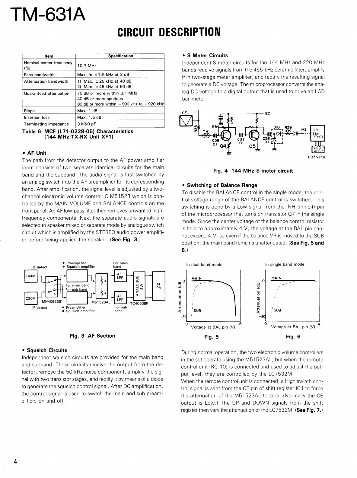
°SMeter Circuits
Independent Smeter circuits for the 144 MHz and 220 MHz
bands receive signals from the 455 kHz ceramic filter, amplify
if in two-stage meter amplifier, and rectify the resulting signal
to generate aDC voltage. The microprocessor converts the ana-
log DC voltage to adigital output that is used to drive an LCD
bar meter.
CFI 8c
DIO R39
IOK
Item Specification
Nominal center frequency
(fo)
10.7 MHz
Pass bandwidth Max. fo +7.5 kHz at 3dB
Attenuation bandwidth 1) Max. +25 kHz at 40 dB
2) Max. +45 kHz at 60 dB
Guaranteed attenuation 70 dB or more within +1 MHz
40 dB or more spurious
80 dB or more within -900 kHz to -920 kHz
Ripple Max. 1dB
Insertion loss Max. 1.5 dB
Terminating impedance 3kQ/0 pF
!
J
CPU
33pin
PTH01
t
ASS Y
©THI M2
c37 NOY C38:
ol
Q5 Le
P33.P30
Fig. 4144 MHz S-meter circuit
¢Switching of Balance Range
To disable the BALANCE control in the single mode, the con-
trol voltage range of the BALANCE control is switched. This
switching is done by aLow signal from the INH (Inhibit) pin
of the microprocessor that turns on transistor Q7 in the single
mode. Since the center voltage of the balance control resistor
is held to approximately 4V, the voltage at the BAL pin can-
not exceed 4V, so even if the balance VR is moved to the SUB
position, the main band remains unattenuated. (See Fig. 5and
6.)
In dual band mode In single band mode
Attenuation (dB)
144M LPF
For main band AF
PA
For sub band qn
220M
MN4066BS' M51523AL TC4053BF
AF
MAIN
SUB
MAIN
suB
os
AF
LPF
For sub
band
084
Voltage at BAL pin (V) Voltage at BAL pin (V)
Fig. 5Fig. 6
During normal operation, the two electronic volume controllers
in the set operate using the M51523AL, but when the remote
control unit (RC-10) is connected and used to adjust the out-
put level, they are controlled by the LC7532M.
When the remote control unit is connected, aHigh switch con-
trol signal is sent from the CE pin of shift register IC4 to force
the attenuation of the M51523AL to zero. (Normally the CE
output is Low.) The UP and DOWN signals from the shift
register then vary the attenuation of the LC7532M. (See Fig. 7.)
4
TM-631A
CIRCUIT DESCRIPTION
Table 6MCF (L71-0228-05) Characteristics
(144 MHz TX-RX Unit XF1)
©AF Unit
The path from the detector output to the AF power amplifier
input consists of two separate identical circuits for the main
band and the subband. The audio signal is first switched by
an analog switch into the AF preamplifier for its corresponding
band. After amplification, the signal level is adjusted by atwo-
channel electronic volume control [C:M51523 which is con-
trolled by the MAIN VOLUME and BALANCE controls on the
front panel. An AF low-pass filter then removes unwanted high-
frequency components. Next the separate audio signals are
selected to speaker mixed or separate mode by analogue switch
circuit which is amplified by the STEREO audio power amplifi-
er before being applied the speaker. (See Fig. 3.)
@Preamplifier For main
IF detect @Squelch amplifier band
IF detect ©Preamplifier
@Squelch amplifier
Fig. 3AF Section
®Squelch Circuits
Independent squelch circuits are provided for the main band
and subband. These circuits receive the output from the de-
tector, remove the 50 kHz noise component, amplify the sig-
nal with two transistor stages, and rectify it by means of adiode
to generate the squelch control signal. After DC amplification,
the control signal is used to switch the main and sub pream-
plifiers on and off.
°SMeter Circuits
Independent Smeter circuits for the 144 MHz and 220 MHz
bands receive signals from the 455 kHz ceramic filter, amplify
if in two-stage meter amplifier, and rectify the resulting signal
to generate aDC voltage. The microprocessor converts the ana-
log DC voltage to adigital output that is used to drive an LCD
bar meter.
CFI 8c
DIO R39
IOK
Item Specification
Nominal center frequency
(fo)
10.7 MHz
Pass bandwidth Max. fo +7.5 kHz at 3dB
Attenuation bandwidth 1) Max. +25 kHz at 40 dB
2) Max. +45 kHz at 60 dB
Guaranteed attenuation 70 dB or more within +1 MHz
40 dB or more spurious
80 dB or more within -900 kHz to -920 kHz
Ripple Max. 1dB
Insertion loss Max. 1.5 dB
Terminating impedance 3kQ/0 pF
!
J
CPU
33pin
PTH01
t
ASS Y
©THI M2
c37 NOY C38:
ol
Q5 Le
P33.P30
Fig. 4144 MHz S-meter circuit
¢Switching of Balance Range
To disable the BALANCE control in the single mode, the con-
trol voltage range of the BALANCE control is switched. This
switching is done by aLow signal from the INH (Inhibit) pin
of the microprocessor that turns on transistor Q7 in the single
mode. Since the center voltage of the balance control resistor
is held to approximately 4V, the voltage at the BAL pin can-
not exceed 4V, so even if the balance VR is moved to the SUB
position, the main band remains unattenuated. (See Fig. 5and
6.)
In dual band mode In single band mode
Attenuation (dB)
144M LPF
For main band AF
PA
For sub band qn
220M
MN4066BS' M51523AL TC4053BF
AF
MAIN
SUB
MAIN
suB
os
AF
LPF
For sub
band
084
Voltage at BAL pin (V) Voltage at BAL pin (V)
Fig. 5Fig. 6
During normal operation, the two electronic volume controllers
in the set operate using the M51523AL, but when the remote
control unit (RC-10) is connected and used to adjust the out-
put level, they are controlled by the LC7532M.
When the remote control unit is connected, aHigh switch con-
trol signal is sent from the CE pin of shift register IC4 to force
the attenuation of the M51523AL to zero. (Normally the CE
output is Low.) The UP and DOWN signals from the shift
register then vary the attenuation of the LC7532M. (See Fig. 7.)
4


 User manual")


 User manual")