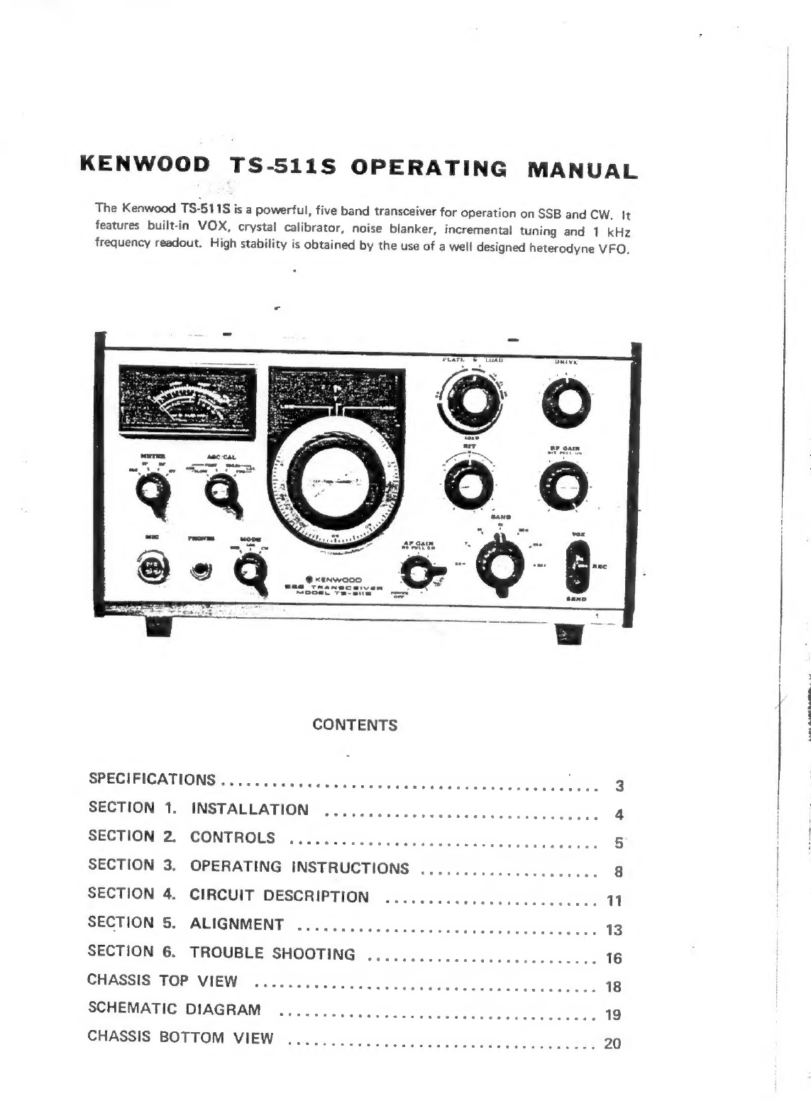
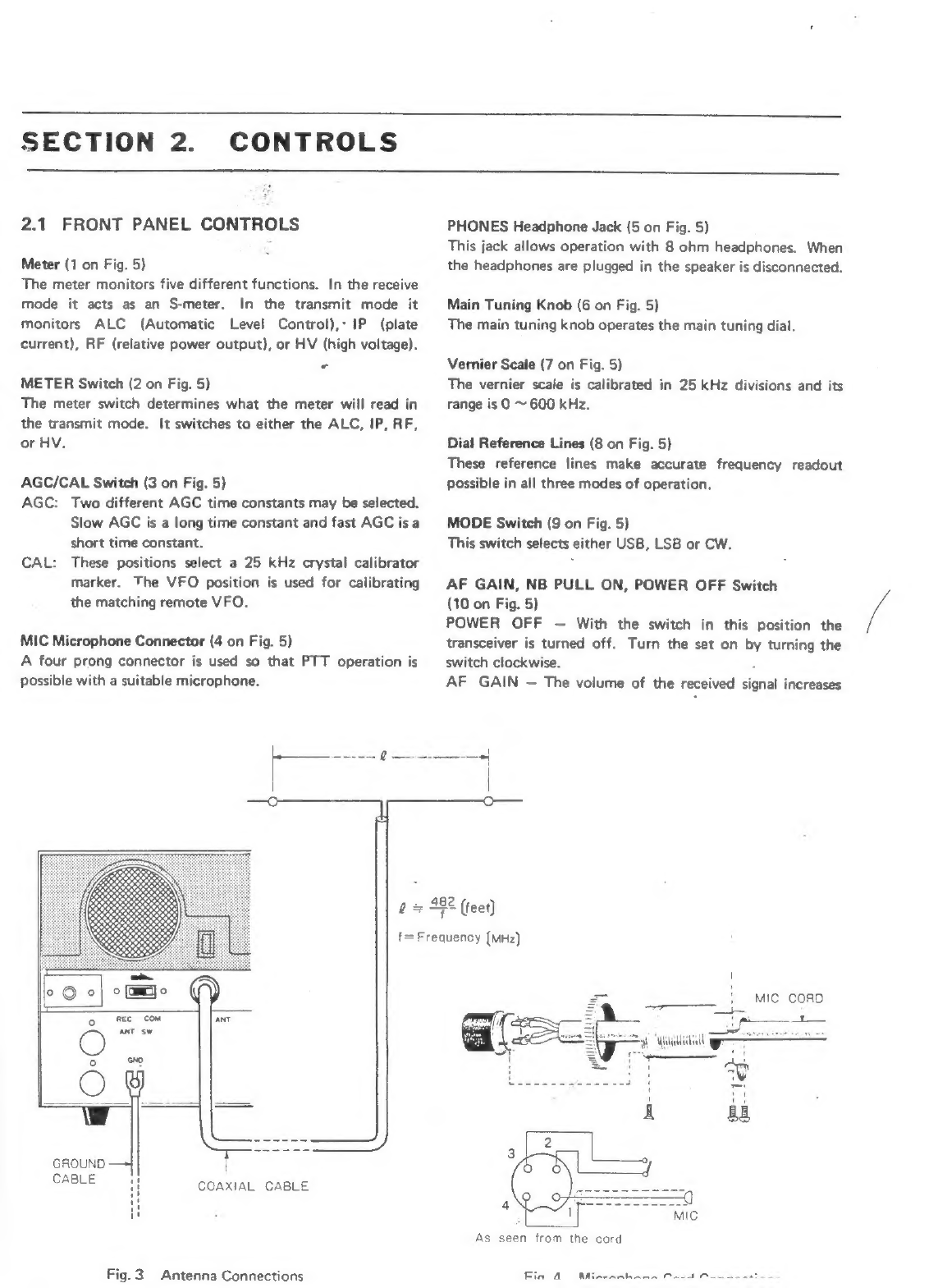
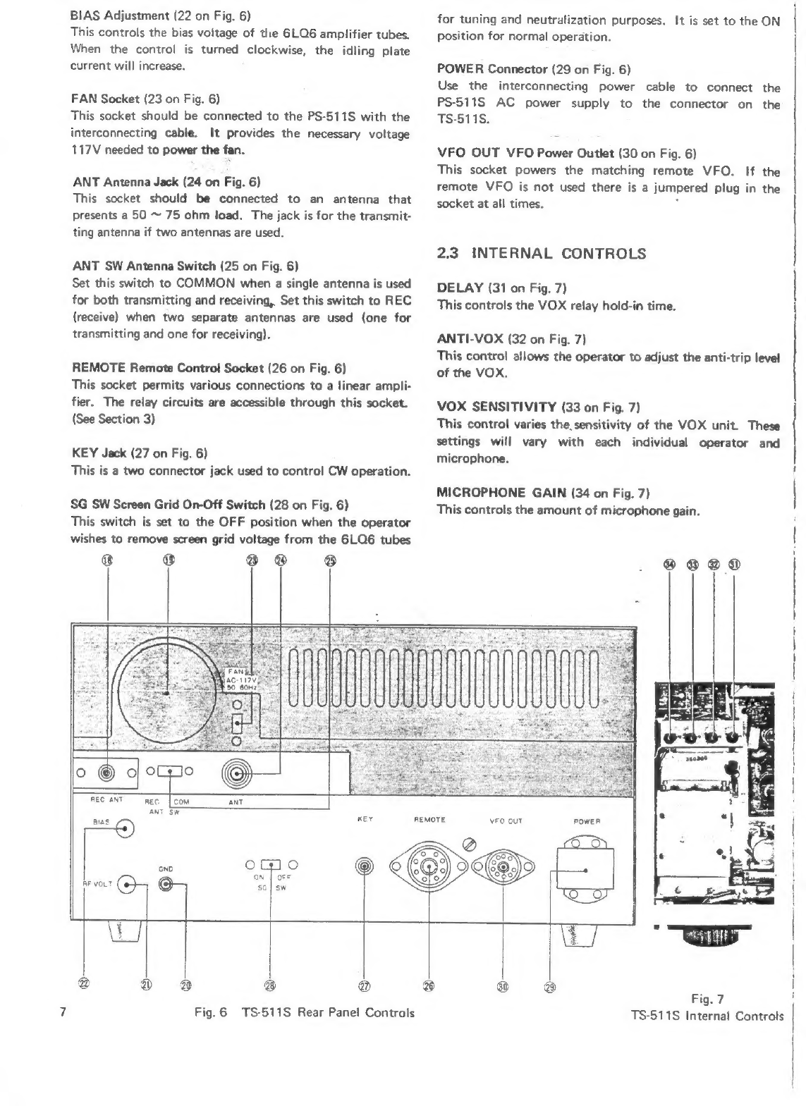
Kenwood TS-511S User manual
Other Kenwood Transceiver manuals

Kenwood
Kenwood TH-D72A User manual

Kenwood
Kenwood TM-221A User manual

Kenwood
Kenwood TS-870S User manual

Kenwood
Kenwood TK-2160 User manual

Kenwood
Kenwood TK-5210 User manual

Kenwood
Kenwood TK-3302 Operating manual

Kenwood
Kenwood TK-868GD User manual

Kenwood
Kenwood TM-221A User manual

Kenwood
Kenwood TS-950 series User manual

Kenwood
Kenwood NEXEDGE NX-411K2 User manual

Kenwood
Kenwood TS-430S User manual

Kenwood
Kenwood TM-3530A User manual

Kenwood
Kenwood TK-630 series User manual

Kenwood
Kenwood NX-320 Series User manual

Kenwood
Kenwood TK-2107G User manual

Kenwood
Kenwood TM-2530A User manual

Kenwood
Kenwood TM-241A User manual

Kenwood
Kenwood TK-2206M User manual

Kenwood
Kenwood TK-3207 User manual

Kenwood
Kenwood TK-7100 User manual