Lanner LVC-5550S User manual

>>
In-Vehicle Computing
Hardware Platforms for Embedded and Industrial Computing
LVC-5550S
V1.1
User's Manual
Publication date:2014-07-01

2
About
About
Embedded and Industrial Computing
Overview
Icon Descriptions
The icons are used in the manual to serve as an indication
of interest topics or important messages. Below is a
description of these icons:
NOTE: This check mark indicates that
thereisa note of interestandissomething
that you should pay special attention to
while using the product.
WARNING: This exclamation point
indicates that there is a caution or
warning and it is something that could
damage your property or product.
Online Resources
The listed websites are links to the on-line product
information and technical support.
Resource Website
Lanner http://www.lannerinc.com
Product Resources http://assist.lannerinc.com
RMA http://eRMA.lannerinc.com
Copyright and Trademarks
This document is copyrighted, © 2013. All rights are
reserved. The original manufacturer reserves the right to
make improvements to the products described in this
manual at any time without notice.
No part of this manual may be reproduced, copied,
translated or transmitted in any form or by any means
without the prior written permission of the original
manufacturer. Information provided in this manual is
intended to be accurate and reliable. However, the original
manufacturer assumes no responsibility for its use, nor for
any infringements upon the rights of third parties that
may result from such use.
Acknowledgement
Intel, Pentium and Celeron are registered trademarks of
Intel Corp.
Microsoft Windows and MS-DOS are registered trademarks
of Microsoft Corp.
All other product names or trademarks are properties of
their respective owners.
Compliances and Certification
CE Certication
This product has passed the CE test for environmental
specifications. Test conditions for passing included the
equipment being operated within an industrial enclosure.
In order to protect the product from being damaged by
ESD (Electrostatic Discharge) and EMI leakage, we strongly
recommend the use of CE-compliant industrial enclosure
products.
FCC Class A Certication
This equipment has been tested and found to comply
with the limits for a Class A digital device, pursuant to Part
15 of the FCC Rules. These limits are designed to provide
reasonable protection against harmful interference when
the equipment is operated in a commercial environment.
This equipment generates, uses and can radiate radio
frequency energy and, if not installed and used in
accordance with the instruction manual, may cause
harmful interference to radio communications. Operation
of this equipment in a residential area is likely to cause
harmful interference in which case the user will be required
to correct the interference at his own expense.
e Mark Certication
E13 - Luxembourg

3
About
About
Embedded and Industrial Computing
Mechanical compliance
Vibration:
General Vibration (operating): Refer to MIL-STD-810G,•
Method 514.6, Procedure I (Transportation), Category
4 – Common carrier (US highway truck vibration
exposure)
General Vibration (non-operating): Refer to MIL-STD-•
810G, Method 514.6, Procedure I (Transportation),
Category 24 – General minimal integrity
Shock:
Operating (Functional Test for Ground Equipment):•
Refer to MIL-STD-810G, Method 516.6, Procedure I,
40g, 11ms
Non-Operating (Crash Hazard Shock Test for Ground•
Equipment): Refer to MIL-STD-810G, Method 516.6,
Procedure V, 75g, 11ms
Electrical transient conduction along supply lines only
(12V/24V)
Revision History
Version Changes
V1.1 Change the DI/DO default BIOS values

TTaTTable of Contentsbeable of Contents
4
Chapter 1: Introduction 5
System Specication . . . . . . . . . . . . . . . . . . . . . . . . . . . . . . . . . . . . . . . . . . . 5
Package Contents . . . . . . . . . . . . . . . . . . . . . . . . . . . . . . . . . . . . . . . . . . . . . 6
Chapter 2: System Components 7
System Drawing . . . . . . . . . . . . . . . . . . . . . . . . . . . . . . . . . . . . . . . . . . . . . . 7
Block Diagram . . . . . . . . . . . . . . . . . . . . . . . . . . . . . . . . . . . . . . . . . . . . . . . 8
Front Components. . . . . . . . . . . . . . . . . . . . . . . . . . . . . . . . . . . . . . . . . . . . . 9
Rear Components . . . . . . . . . . . . . . . . . . . . . . . . . . . . . . . . . . . . . . . . . . . . .11
Chapter 3: Board Layout 12
External Connectors. . . . . . . . . . . . . . . . . . . . . . . . . . . . . . . . . . . . . . . . . . . .12
Internal Connectors and Jumpers . . . . . . . . . . . . . . . . . . . . . . . . . . . . . . . . . . .13
Connectors and Jumpers List. . . . . . . . . . . . . . . . . . . . . . . . . . . . . . . . . . . . . .14
Jumper Settings . . . . . . . . . . . . . . . . . . . . . . . . . . . . . . . . . . . . . . . . . . . . . .15
Chapter 4: The Flow Chart 20
Chapter 5: Hardware Setup 21
Preparing the Hardware Installation. . . . . . . . . . . . . . . . . . . . . . . . . . . . . . . . . .21
System Memory Installation. . . . . . . . . . . . . . . . . . . . . . . . . . . . . . . . . . . . . . .21
CompactFlash Card Installation. . . . . . . . . . . . . . . . . . . . . . . . . . . . . . . . . . . . .21
3G and Wireless Module Installation . . . . . . . . . . . . . . . . . . . . . . . . . . . . . . . . .21
3G SIM Card Installation . . . . . . . . . . . . . . . . . . . . . . . . . . . . . . . . . . . . . . . . .22
External SIM Card Installation . . . . . . . . . . . . . . . . . . . . . . . . . . . . . . . . . . . . . .22
Hard Disk Installation . . . . . . . . . . . . . . . . . . . . . . . . . . . . . . . . . . . . . . . . . . .22
Connecting Power . . . . . . . . . . . . . . . . . . . . . . . . . . . . . . . . . . . . . . . . . . . . .23
Appendix A: Using the Ignition System Manager (ISM) 24
Appendix B: Digital Input/Output 25
Appendix C: Accessing the GPS Data from the LVC-5550S 31
Appendix D: Programming System Watchdog Timer of the LVC-5550S 36
Appendix E: Terms and Conditions 40
Warranty Policy . . . . . . . . . . . . . . . . . . . . . . . . . . . . . . . . . . . . . . . . . . . .40
RMA Service . . . . . . . . . . . . . . . . . . . . . . . . . . . . . . . . . . . . . . . . . . . . . .40

5
Introduction
Chapter 1
Embedded and Industrial Computing
Chapter 1:
Introduction
Thank you for choosing the LVC-5550S. The LVC-5550S is
an ultra-robust embedded system which equips with a
suspension kit to eliminate shock and vibration when is
it installed on a moving transportation system.
The system encompasses a wide variety of communication
ports to facilitate every possible in-vehicle applications
including surveillance, event data recorder and the GPS
system. It also features an external HDD drive for easy
insertion of the HDDs. The following list highlights the
capabilities of the LVC-5550S system:
1x Mic-in and Line-out (for PC)•
One Digital I/O port for digital input and output•
connections
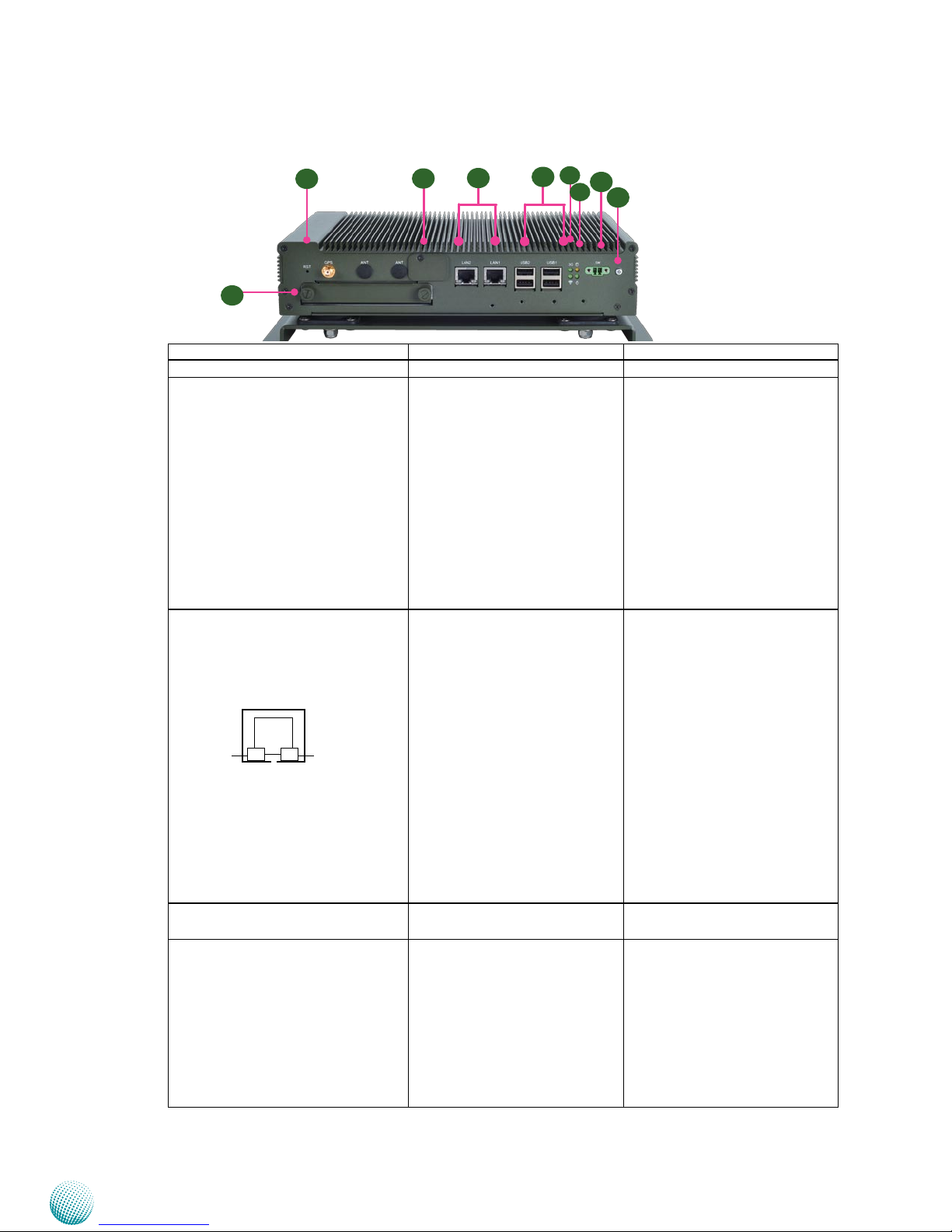
Rich I/O ports: 2 RS-232/422/485 and 1 RS-232, 2 LAN•
ports, 4 USB ports, Digital input/output ports
Triple video display: LVDS (optional) and DVI-D and•
VGA output with Intel graphic engine GMA 3650
Power ignition control mechanism with programmable•
on/off/delay switch
Wide range of DC power input from 9V to 30V, suitable•
for vehicular 12V or 24V battery with Ignition control.
–Power input current protection by the 10A fuse and
15KP30A TVS
--12V DC output current protection by the 1A Polyfuse
Battery voltage protection: Over Voltage Protection•
and Under Voltage Protection
Standby power consumption are well under 12V/12mA
and 24V/10mA
Extended operating temperature between -5ºC ~ 45•
ºC (23 ~ 113ºF)
System Specification
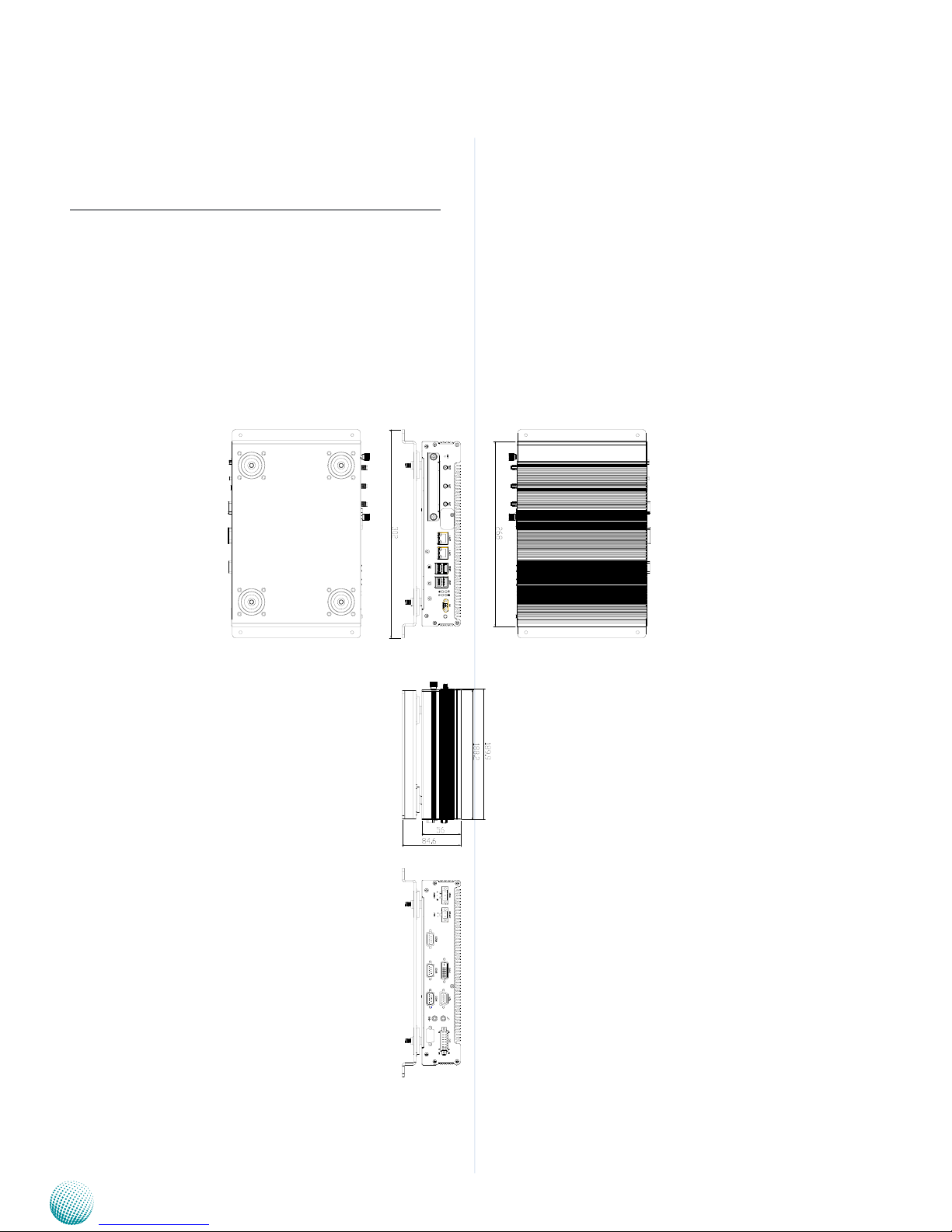
Dimensions (WxHxD) 268x84x190mm
(10.55”x3.31”x7.48”)
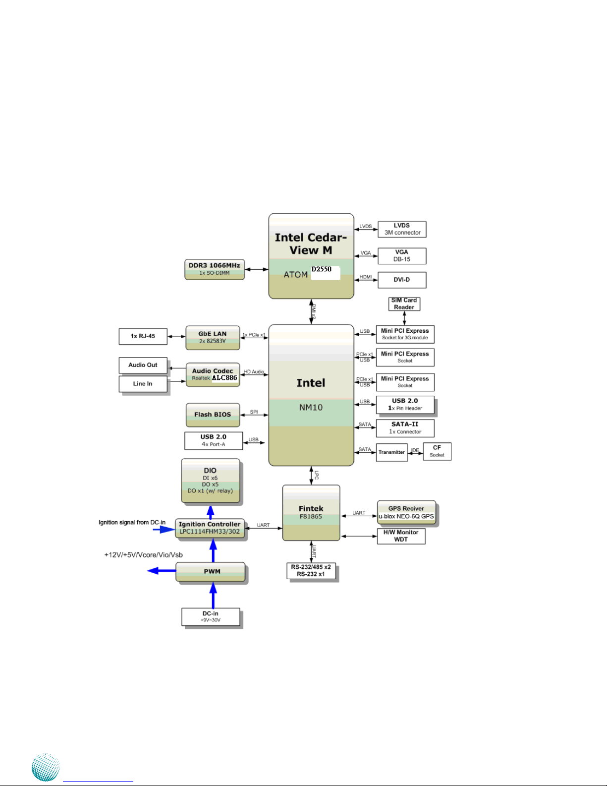
Processor Intel Atom D2550 Processors
Chipset Intel NM10
System
Memory
Technology DDR3 SODIMM x1
Max. Capacity Up to 4GB
Storage IDE CF socket Type I/II x1
SATA External 2.5” SSD/HDD drive bay
Ethernet Controller Intel 82583V x2
Graphic Controller Intel integrated GMA3650 engine
Audio Controller Realtek ALC886 HD Codec
IO
LAN GbE RJ45 x2
Display
DB15 x1 for VGA, DVI-D x1, Op-
tional LVDS (integrating USB,
12V and remote power switch)
Audio 1x Mic-in and Line-out (for PC)
Serial I/O
DB9 Male x2 supports RS-232/485
with RI/5V/12V
DB9 Male x1 supports RS-232
GPS U-blox NEO-6Q GPS
Digital I/O
4x DI 12V Level
3x DO 12V Level
2x DI (from MCU) 3.3V Level, 1x
relay (2A, 12V/24V)
USB 2.0 Type A x4
Power Input 3-pin terminal block (+, -, ignition)
Expansion
Mini-PCIex3 (full-size Mini-PCIe
socket x2 and half-size Mini-PCIe
socket x1)
Others 3x SMA antenna hole
Power Input
DC Input: 9~30V for +12V-level and
+24V-level car battery
Ignition Control: Support igni-
tion on/off and delay Power-on/
off system, time frame by software
setting
Remote power-on via DI (from MCU)
detection
Power Output 12V (Max 1A)
AC Adapter Ordering Option
Hardware Monitor Fintek F81865 integrated watchdog
timer 1~255 level
OS Support XPE/WES2009, XP Pro FES, WS7E,
WS7P, Win 7 Pro FES
Certications CE, FCC Class A, E13, RoHS
Compliance Vibration & Shock: MIL-STD-810G

6
Introduction
Chapter 1
Embedded and Industrial Computing
Package Contents
Your package contains the following items:
LVC-5550S Fanless Embedded System with a•
Suspension Kit
3G audio internal cable (optional,•
P/N: 080W1C0901001)
Drivers and User’s Manual CD (P/N: S09OAD826H100)•
Female Terminal Block Connectors•
(P/N: 04AW20021E101
04AW20023Z101
04AW20031E001
04AW20161Z101)
GPS Receiver Antenna (P/N: 080W0Q0001501)•
HDD Screws x 2 (P/N: 070W102400603)•
Operating
Tempera-
ture
Range
With Industrial
Components -30~60°C/-22~140°F
With Com-
mercial
Components -5~45°C / 23~113°F

7
System Components
Chapter 2
Embedded and Industrial Computing
Chapter 2:
System Components
System Drawing
Mechanical dimensions of the LVC-5550S with the
suspension kit
Unit: mm

8
System Components
Chapter 2
Embedded and Industrial Computing
Block Diagram
The block diagram depicts the relationships among the
interfaces and modules on the motherboard..

9
System Components
Chapter 2
Embedded and Industrial Computing
Front Components
Component Description Pin Definition Reference
F1 Reset Switch A hardware reset button RSTSW1 on page 18
F2 External SIM Card Reader with a
Cover External SIM Card Reader for
3G wireless Internet service.
The system supports dual 3G
Internet service with two SIM
card reader. This SIM card reader,
together with its internal PCIe
expansion (MCARD1) supports
3G voice service. Recommended
3G module: Sierra MC8090/8092
(power voltage 3.6V). There
is also a jumper setting for
enabling or disabling the 3G
SMS/Ring wake-up.
F3 Two 10/100/1000Mbps LAN
ports Two RJ-45 (network) jacks with
LED indicators as described
below
LINK/ACT (Yellow)
On/Flashing: The port is•
linking and active in data
transmission.
Off: The port is not linking.•
SPEED (Green/Amber)
Amber: The connection•
speed is 1000Mbps.
Green: The connection•
speed is 100Mbps
Off: .The connection speed•
is 10Mbps.
LANB1/LANB2 on page 17
F4 Four USB 2.0 Ports An USB type A connector• Dual USB Port Connector 0 and 1
(USB1, USB2) on page 16
F5 3G and
Wi-Fi LED
3G LED (Green)
Blinking: 3G wireless Internet is
active
Off: The 3G wireless Internet is
inactive.
Wi-Fi LED (Green)
Blinking: The Wi-Fi is active
Off: The Wi-Fi is not active
LED2 on page 18
F1 F2 F3 F4 F7
F5
F6
LINK/ACT
SPEED
F8
F9

10
System Components
Chapter 2
Embedded and Industrial Computing
Component Description Pin Definition Reference
F6 HDD (Yellow) and
Power LED (Green)
HDD
Blinking: data access•
activities
Off: no data access•
activities
Power
On: The computer is on.•
Off: The computer is off .•
LED1 on page 18
F7 External Power Switch through
terminal block A Power on/off switch
connector.
Short Press:• Power o the
system with the proper
procedure just like the
shutdown program on
Windows.
Long Press: Power o the•
system without the proper
procedure, i.e., force to
shutdown (reserved func-
tion for systems without
power ignition control.
CN1 on page 17
F8 Power-on Button with Dual LED ATX power-on button with LEDs:
stand-by mode in red; power-
on mode in green.
PSBTN1 on page 18
F9 Hard Disk Slot External SATA hard disk drive for
easy access and replacement of
the data storage.
SATA1 (data) and CON2 (SATA
power) on page 15

11
System Components
Chapter 2
Embedded and Industrial Computing
Rear Components
Component Description Pin Definition Reference
R1 Power-In (DC) Power-in with ignition support. The
LVC-5550S support a wide range of
power input (+9V ~ +30) including
the prevalent 12V and 24V vehicular
power system. It has a 2KV ESD
protection on the DC input and
ignition line.
DC_IN1 Connector (DC_IN1) on
page 16
R2 Power Output (DC) Power output of 12VDC CN6 on page 17
R3 DVI-D Port A DVI-D port (single link) which
is provided by Intel GMA 3650
(resolution: 1920x1200).
DVI1 on page 17
R4 VGA Port It connects an external VGA monitor
or projector (resolution: 1920x1200) VGA1 on page 17
R5 Line-out and Mic-in Port Connect audio devices to these port.
They are provided by Realtek ALC 886
HD audio codec
AUDIO1 on page 16
R6 DIO Port The general-purpose input/output1
(GPIO) peripheral provides dedicated
general-purpose pins for 6 input
and 6 output controls. The digital
input helps triggering between
open and closed circuit such as PIRs,
door/window contact, glass break
detector. And the output can connect
to devices such as relays and LEDs.
DGIOC1 on page 16
R7 Serial Ports (from left to right:
COM3/COM2/COM1)
COM1 and COM2 provide RS232/
RS422/RS485 communications with
a dip switch selecting among these
standards.
COM3 provides RS232 serial
communication only.
RS-232 COM Port (COM3, COM2,
COM1) on page 15
R3
R2R1 R6
R4 R5
R7
COM3 COM2 COM1

12
Board Layout
Chapter 3
Embedded and Industrial Computing
Chapter 3:
Board Layout
External Connectors
The following picture highlights the location of system
input/output connectors. Refer to the table 3.1 Connector
List for more details.
LANB2/LANB1 LED2/LED1
SIM1
RSTSW1
AUDIO1
DGIOC1
COM2
DVI
COM1
VGA
CN6
DC_IN1
LVDSC1
COM3
USB2/USB1 PSBTN1
CN1
3GAUDC1

13
Board Layout
Chapter 3
Embedded and Industrial Computing
Internal Connectors and Jumpers
The following picture highlights the location of internal
connectors and jumpers. Refer to the table 3.1 Connector
List for more details.
MCARD1
SW2
SW5
3GAUDC1 CCMOS1 CF1
LVB-5550
CN2
SW3 SW4
PCOM1
PCOM2
MPCIE2
MPCIE1
SW6 SATA1
PCOM3 KM1
CON2
SW1
JSPIROM1
DLPC1
CN4
PMCAR2
PMCAR1
SIM1

14
Board Layout
Chapter 3
Embedded and Industrial Computing
Connectors and Jumpers List
The tables below list the function of each of the board
jumpers and connectors by labels shown in the above
section. The next section in this chapter gives pin
definitions and instructions on setting jumpers.
Table 3.1 Connector List for LVB-5550
Labels Function Pin Denition Reference Page
3GAUDC1 3G voice MIC-in and ear out connector P18
AUDIO1 Line out and MIC-in audio connector P16
CCMOS1 Clear CMOS jumper P16
CF1 CompactFlash connector P16
CN1 External power button connector P17
CN2 204 Pin DDR3 SO-DIMM Socket
CN4 External RS-232 programming connector for
the MCU
P19
CN6 12V DC power-out connector P17
COM1 COM Port 1 P15
COM2 COM Port 2 P15
COM3 COM Port 3 P15
CON2 2.5" SATA HDD power connector P15
DC_IN1 9V~30V DC power-in connector with ignition P16
DGIOC1 6bit Digital Input/Output P16
DLPC1 LPC port 80 debugging port Reserved for factory use
DVI1 DVI-D connector P17
JSPIROM1 SPI ROM BIOS downloading cable connector Reserved for factory use
KM1 PS/2 keyboard and mouse P16
LANB1/LANB2 RJ-45 port with LED indicator P17
LED1 Power LED and HDD LED P18
LED2 Wi-Fi LED and 3G Wi-Fi LED P18
LVDSC1 18bits LVDS connector with USB signal and
power button
P18
MCARD1 PCIe connector for Sierra 3G USB type Wi-Fi
module
P18
MPCIE1/2 1x mini PCIe connector (Version 1.2) P17
PCOM1/2/3 Select COM1/COM2/COM3 Pin 9 function P15
PSBTN1 Power button P18
RSTSW1 System reset button P18
SATA1 SATA connector P15
SW1,SW2 Select MCU function P19
SW3 Enable/disable COM1 termination P15
SW4 Select COM1 type P15
SW5 Select COM2 type P15
SW6 Enable/disable COM2 termination P15
USB1/USB2 USB port P16
VGA1 VGA1 connector P17

15
Board Layout
Chapter 3
Embedded and Industrial Computing
Enable/disable termination for COM1/COM2 (SW3/
SW6): Enable the COM1/COM2 termination at RS-422 or
RS-485 mode
RS-485 terminating resistance RX on
RS-232 COM Port 3 (COM3): COM3 port is an RS-232
serial port.
PCOM1/2/3: Select COM1/COM2/COM3 Pin9 Function
(in RS-232). The Ring indicator pinout of the RS-232 COM
port can be altered according to the following jumper
settings.
Jumper Settings
Serial-ATA Connector (SATA1): It is for connecting a 2.5’’
SATA SSD to be served as your system’s storage. It can
support SATA II which features Data transfer rates up to
3.0 Gb/s (300 MB/s).
4-pin Serial-ATA Power Connector (CON2): It is for
connecting the SATA power cord.
COM Port 1/2 (COM1/COM2): COM1/COM2 ports are
serial ports which are selectable among RS-232/422/485
standards.
RS-232/422/485 Pinout:
Select COM1/COM2 Type Switch (SW4/SW5):
Pin No. Pin Name
RS-232 RS-422 RS-485
1 DCD TxD- Data-
2 RXD TxD+ Data+
3 TXD RxD+
4 DTR RxD-
5 GND Signal Ground
6 DSR
7 RTS
8 CTS
9 RI/5V/12V
COM1 TYPE Description
RS-232 (Default) 1-ON, 2-OFF, 3-OFF, 4-OFF
RS-422 1-OFF, 2-ON, 3-ON, 4-OFF
RS-485 1-OFF, 2-ON, 3-OFF, 4-ON
Pin No. Function
1-2 Ring-in (default)
3-4 Supply +5V to Device
5-6 Supply +12V to Device
LVB-5550 (V1.0)
Pin No. Function Pin No. Function
1 DCD 2 RXD
3 TXD 4 DTR
5 GND 6 DSR
7 RTS 8 CTS
9 RI/5V/12V
Pin No. Function
1 NC
2 Ground
3 Ground
4 VCC(5V)
Pin No. Function
1 GND
2 TX+
3 TX-
4 GND
5 RX-
6 RX+
7 GND
7
6
5
4
3
2
1
4 3 2 1
RS-232 (default)
4321
ON
RS-422
4321
RS-485
Pin No. Description
1-OFF, 2-OFF,
3-OFF, 4-OFF
Terminating resistance OFF
1-ON, 2-ON,
3-ON, 4-ON
RS-422/RS-485 Terminating resistance Tx, Rx on
1-ON, 2-ON
3-OFF, 4-OFF
RS-485 terminating resistance RX on
Terminating resistance off
1 2 3 4
ON
RS-422 or RS-485 terminating resistance TX, RX on
1 2 3 4
ON
1 2 3 4
ON
6 7 8 9
1 2 3 4 5
5
3
1
6
4
2
6 7 8 9
1 2 3 4 5 2 4 6 8 10
1 3 5 7 9
PCOM1/PCOM2 PCOM3
1 3 5
2 4 6
SW4 SW5
4321
ON
4
3
2
1
4
3
2
1
4
3
2
1
SW3 SW6
ON
1
2
3
4
1
2
3
4
ON
ON
1
2
3
4

16
Board Layout
Chapter 3
Embedded and Industrial Computing
Pin No. Function Pin No. Function
1 GND 26 CF_CD1#
2 CF_DD3 27 CF_DD11
3 CF_DD4 28 CF_DD12
4 CF_DD5 29 CF_DD13
5 CF_DD6 30 CF_DD14
6 CF_DD7 31 CF_DD15
7 CF_DCS0# 32 CF_DCS1#
8 A10(GND) 33 VS1#
9 OE#(GND) 34 CF_DIOR#
10 A9(GND) [CF_SATA_RXP] 35 CF_DIOW#
11 A8(GND) [CF_SATA_RXN] 36 WE#(VCC3)
12 A7(GND) 37 CF_IRQ#
13 VCC 38 VCC
14 A6(GND) 39 CSEL#(GND)
14 A5(GND) [CF_SATA_TXN] 39 VS2#
15 A4(GND) [CF_SATA_TXP] 40 CF_RESET#
16 A3(GND) 41 CF_IORDY
17 CF_A2 42 CF_DMARQ
18 CF_A1 43 CF_DDACK#
19 CF_A0 44 CF_ACT#
20 CF_DD0 45 CF_DIAG
21 CF_DD1 46 CF_DD8
22 CF_DD2 47 CF_DD9
23 WP(NC) 48 CF_DD10
24 CF_CD2# 49 GND
25 CD2# 50 GND
Dual USB Port Connector 0 and 1 (USB1, USB2)
Line-Out and MIC-In Connector (AUDIO1):
PS/2 Keyboard & Mouse Connector (KM1):
DC_IN CONNECTOR (DC_IN1): A Phoenix connector for
external power supply with ignition.
Digital IN/OUT(DGIOC1) Connector: The 12 pins of
General Purpose Input/Output (GPIO) support input and
output operations through the terminal block.
Maximum input/output current for each port is
100mA
Input/output
pins:
DI_0/DI_1/
DI_2/DI_3
DO_0/DO_1/
DO_2/DO_3
Voltage Logic Register
Di: <0.8V
Do: <0.4V
Low 0
DI: 10 ~ 12V
Do:12V
High 1
DI_4/DI_5
(only low
status can be
detected for
MCU control)
<0.8V Low 0
3.3V High 1
The default BIOS value:
0 for DI_0~DI_3, 1 for DI_4~DI_5, and 1 for DO.
Pin15 (Relay_NOPEN) and pin16 (Relay_COMM) On/
O can be used for control of MCU DO_1: out 1(high)=
on; out 0(low)=o.
Clear CMOS jumper (CCMOS1): It is for clearing the
CMOS memory.
CompactFlash Connector (CF1): It is for connecting a
Compact Flash card to be served as your system’s storage.
Pin No. Function
1-2 Normal (Default)
2-3 Clear CMOS
1 2 3
25 1
50 26
Pin No. Function
1 USB power1_+5V
2 USB1_DAT-
3 USB1_DAT+
4 Ground
5 USB power0_+5V
6 USB0_DAT-
7 USB0_DAT+
8 Ground
Pin No. Function
1 GND_AUD
2 MIC_IN_L
3 GND_AUD
4 GND_AUD
`5 MIC_IN_R
Pin No. Pin Name
1 Ignition in
2 GND
3 9V~30V DC IN
3 2 1
1 2 3 4
5 6 7 8
Pin No. Pin Name
1 KBCLK
3 KEY
5 KEY
7 MSCLK
Pin No. Pin Name
2 GND
4 KBDAT
6 MSDATA
8 +5V
2 4 6 8
1 3 5 7
Pin No. Pin Name Pin No. Pin Name
1 DI_0 2 DO_0
3 DI_1 4 DO_1
5 DI_2 6 DO_2
7 DI_3 8 DO_3
9 DI_4 10 NC
11 DI_5 12 NC
13 GND 14 GND
15 Relay_
NOPEN
16 Relay_
COMM
MIC-in Pink Jack Line-out Lime Jack
Pin No. Function
1 LINE_OUT_L
2 GND_AUD
3 GND_AUD
4 LINE_OUT_ R

17
Board Layout
Chapter 3
Embedded and Industrial Computing
DVI-D Connector (DVI1): The video display is powered by
Intel®GMA 3650 graphics engine.
VGA in DB-15 connector (VGA1): It is used for connecting
a VGA monitor.
Power-Out Connector (CN6): 12V DC Power-out
connector.
External Power Button Connector(CN1): An external power
button for distance power on/off control.
LAN1/LAN2 Ports (LANB1/LANB2)
Pin No. Description
Fast Ethernet Gigabit Ethernet
1 TX+ MD0+
2TX- MD0-
3 RX+ MD1+
4 T45 MD2+
5 T45 MD2-
6RX- MD1-
7 T78 MD3+
8 T78 MD3-
Pin No. Pin Name Pin No. Pin Name Pin No. Pin Name
1 Red 6 GND 11 NC
2 Green 7 GND 12 DDC DAT
3 Blue 8 GND 13 HSYNC
4 NC 9 VGA Power 14 VSYNC
5 GND 10 GND 15 DDC CLK
Pin No. Pin Name
1 12V DC-out
2 GND
Mini PCI Express Connector (MPCIE1/MPCIE2): It supports
mini-PCIe V1.2, but not V1.1.
PIN DESCRIPTION PIN DESCRIPTION
1 WAKE# 2 +3.3V
3 RSV1 4 Ground
5 RSV2 6 +1.5V
7 CLKREQ# 8 UIM_PWR
9 Ground 10 UIM_DATA
11 REFCLK- 12 UIM_CLK
13 REFCLK+ 14 UIM_RESET
15 GND3 16 UIM_VPP
KEY KEY
17 RSV3 18 Ground
19 RSV4 20 W_DISABLE#
21 GND5 22 PERST#
23 PERn0 24 +3.3V
25 PERp0 26 Ground
27 Ground 28 +1.5V
29 Ground 30 SMB_SLK
31 PETn0 32 SMB_DATA
33 PETp0 34 Ground
35 Ground 36 USB_D-
37 Ground 38 USB_D+
39 +3.3V 40 Ground
41 +3.3V 42 LED_WWAN#
43 Ground 44 LED_WLAN#
45 RSV9 46 LED_WPAN#
47 RSV10 48 +1.5V
49 RSV11 50 Ground
51 RSV12 52 +3.3V
Note:
MPCIE2 (Mini PCIe half card size)doesn’t come1.
with a SIM card reader; instead, it is used for Wi-
Fi module. It supports 3.3V power supply and
both USB and PCIe signal card type.
MPCIE1 comes with a SIM card reader; it can be2.
used for 3G service connection. It supports 3.3V
power supply and both USB and PCIe signal
card type.
2 1
VGA1
5
1
10 6
15 11
P i n
No.
Function P i n
No.
Function P i n
No.
Function
1 TMDS Data 2¬ 9 TMDS Data 1¬ 17 TMDS Data 0¬
2 TMDS Data 2+ 10 TMDS Data 1+ 18 TMDS Data 0+
3 TMDS Data 2/4 shield 11 TMDS Data 1/3 shield 19 TMDS Data 0/5 shield
4 NC 12 NC 20 NC
5 NC 13 NC 21 NC
6 DDC CLOCK 14 5V 22 TMDS CLK shield
7 DDC DATA 15 GND 23 TMDS CLK+
8 NC 16 HOT PLUG DET 24 TMDS CLK-
Pin No. Pin Name
1 GND
2 Power Button-
1 2

18
Board Layout
Chapter 3
Embedded and Industrial Computing
Power button (PSBTN1): power button with dual LED
which behaves like:
Red: System standby
Green: System power-on
Power LED and HDD LED (LED1): Power LED is in green
color while HDD LED is in yellow color.
3G voice MIC-in and EAR-out Connector (3GAUDC1)
System Reset Button (RSTSW1)
3G and Wi-Fi LED (LED2)
18-bits LVDS Connector with USB signal and power but-
ton (LVDSC1)
PIN NO. DESCRIPTION PIN NO. DESCRIPTION
1 GND 14 LVDS_TX0_DP
2 GND 15 LVDS_TX0_DN
3 Power button 16 BKLT_ON
4 LVDS_TX1_DP 17 GND
5 LVDS_TX1_DN 18 Power status (PU5V)
6 LVDS_TX2_DP 19 GND
7 LVDS_TX2_DN 20 USB_P4_DP
PIN NO. DESCRIPTION PIN NO. DESCRIPTION
8 GND 21 USB_P4_DN
9 +12V 22 LVDS_CLK_DP
10 GND 23 LVDS_CLK_DN
11 +12V 24 +12V
12 LVDS_TX3_DP 25 GND
13 LVDS_TX3_DN 26 LVDS_VEN
Mini Card Connector(MCARD1) for USB type PCIe
connector: for connecting with the 3G module with the
external SIM card (SIM1). This connector also supports
3G voice service. Recommended 3G module: Sierra
MC8090/8092 with power voltage 3.6V.
PIN DESCRIPTION PIN DESCRIPTION
1 NC 2 +3.6V / +3.3V
3 NC 4 Ground
5 NC 6 NC
7 NC 8 USIM_PWR
9 Ground 10 USIM_DATA
11 NC 12 USIM_CLK
13 NC 14 UIM_RESET
15 Ground 16 NC
KEY KEY
17 NC 18 Ground
19 NC 20 W_DISABLE#
21 GND 22 NC
23 NC 24 +3.6V / +3.3V
25 NC 26 Ground
27 Ground 28 NC
29 Ground 30 NC
31 NC 32 WAKE_N
33 RESET_N 34 Ground
35 Ground 36 USB_D-
37 Ground 38 USB_D+
39 +3.6V / +3.3V 40 Ground
41 +3.6V / +3.3V 42 LED_WWAN#
43 Ground 44 GPIO1
45 PCM_CLK 46 GPIO3
47 PCM_DIN 48 GPIO2
49 PCM_OUT 50 Ground
51 PCM_SYNC 52 +3.6V / +3.3V
Note:
The power pin of the MCARD1 connector can1.
be selected between 3.3V and 3.6V via the
following jumper (PMCAR1)
The 3G SMS/Ring wake-up function can be2.
enabled or disabled via the following PMCAR2
jumper.
The connector supports only USB signal card3.
type.
Select MCARD1 Module Voltage Type (PMCAR1): The
default is 3.3V for most 3G mini card; for Sierra Airprime
HSPA+ mini card , set it to +3.6V.
Select MCARD1 Module Wake up Function (PMCAR2):
Pin No. Pin Name Pin No. Pin Name
PAD1 Ground PAD2 Ground
1 Ground 3 Power BUTTON-
2 Ground 4 Power BUTTON-
L1 PWR_LED+ / STB_LED- L2 PWR_LED- / STB_LED+
Pin No. Pin Name Pin No. Pin Name
A1 PWR_LED+ C1 PWR_LED-
A2 HDD_LED+ C2 HDD_ACT¬
Pin No. Pin Name
1 3G_MIC_INR-
2 3G_MIC_INR+
3 GND_AUD1
4 GND_AUD1
5 3G_EAROR-
6 3G_EAROR+
1
3
2
4
Pin No. Pin Name
1 Rset signal
2 GND
3 GND
4 GND
Pin No. Pin Name Pin No. Pin Name
A1 WiFi_LED+ C1 WiFi_LED -
A2 3G WiFi_LED+ C2 3G WiFi_LED -
6
4
2
5
3
1
Pin No. Pin Name
1-3, 2-4 +3.6V
3-5, 4-6 +3.3V (Default)
3
2
1
Pin No. Pin Name
1-2 Enable
2-3 Disable (Default)

19
Board Layout
Chapter 3
Embedded and Industrial Computing
Select MCU Detect Function for power ignition
behavior (SW1):
The function of the above jumpers are further explained
here.
Power Good Detection1. : A power-good signal
from the main board will be sent to the ignition
controller so that the ignition controller can
decide or alter the power state upon the following
instances. (Refer to the flow chart in Chapter 4):
Power-on instance•
Power-good signal turned-low instance•
Low Voltage Detection2. : Turn on this switch to
enable the automatic detection of low voltage
state of the battery. It will automatically turn
off the system when low voltage state has been
detected (Note:the low-voltage condition needs
to remain 30 seconds continually). The voltage
level can be set in the Ignition System Manager
(ISM) which is provided by Lanner as a sample
code for functions on the power ignition module.
The default setting of this function: Shutdown
Voltage in the ISM is disabled. (Refer to the flow
chart in Chapter 4 and the Using the Ignition
System Manager (ISM) in Appendix A.)
Watchdog:3. Enable this switch to enable shutdown
after watchdog timer count-down to zero. This is a
programmable function. If there is no program to
control and monitor the watchdog timer, set this
jumper to disabled to avoid abnormal shutdown.
(Refer to the flow chart in Chapter 4)
MCU (Microcontroller) Function Selection (SW1, SW2):
It is for selecting the microcontroller’s function.
Select Connect MCU communication Port From
Internal or External (SW2): Note the external port is the
CN4 connector (see below) on the board.
An external RS-232 connector for MCU programming
(CN4)
SW1
ON
1
2
3
4
SW2
ON
4 3 2 1
Jumper Pin No. Pin NO.
SW1 1-OFF, 2-OFF, 3-OFF, 4-ON 1-ON, 2-OFF, 3-OFF, 4-OFF
SW2 1-OFF, 2-OFF, 3-ON, 4-ON 1-ON, 2-ON, 3-OFF, 4-OFF
Function Download Data Normal (Default)
Switch 1
Pin No. Pin Name Pin No. Pin Name
1 P2_RT_1 5 GND
2 P3_S0_2 6 IGN3V3_SB
3 P3_S0_1 7 IGN3V3_SB
4 PIO0_1 8 IGN3V3_SB
ON
SW1
1
2
3
4
8
7
6
5
Switch 2
Pin No. Pin Name Pin No. Pin Name
1 PIO1_6_RXD 5 NXP_TXD
2 PIO1_7_TXD 6 NXP_RXD
3 PIO1_6_RXD 7 COM5_RXD
4 PIO1_7_TXD 8 COM5_TXD
Pin No. Pin Name
1,2 ON Connection through internal COM port
(COM5)
3,4 ON Connection through external COM port
(CN4)
ON
4 3 2 1
5 6 7 8
Pin No. Pin Name
1 EXT_TXD
2 GND
3 EXT_RXD
3 2 1
Selector No. SW1 Ignition Function
1 Power Good Detection ON: Enable
OFF: Disable
2 Low Voltage Detection
3 Watchdog
4 Programming MCU Reserved
The default value is ON for selector 1, OFF for se-
lector 2, Off for selector 3, and OFF for selector 4

20
Flow Chart
Chapter 4
Embedded and Industrial Computing
Chapter 4:
The Flow Chart
The flow chart section contains all flow chart used in the
system. The flow chart describes the system’s behavior on
powering on and off the system via power ignition control
or on/off switch when the appropriate timer control
parameters are set.
Note:
For power-good and low-voltage
1.
mechanism to function in the workflow,
you will need to enable the power-good
and low-voltage detection function with
selector 1 and selector 2 of jumper SW1
respectively of the LVB-5550 board.
(Refer to Chapter 3 Board Layout).
For power on and power off delay timer2.
parameter, refer to Appendix A Using the
Ignition System Manager (ISM).
When the system’s shutdown timer starts3.
counting down 180sec, using ignition
or External PWR_BTN to start the system
again during shutdown process will not
work until the countdown finishes.
Table of contents
Other Lanner Desktop manuals

Lanner
Lanner LEC-2530 User manual

Lanner
Lanner LVC-5000-B0 User manual

Lanner
Lanner LEC-6021A User manual

Lanner
Lanner LEC-6032C User manual

Lanner
Lanner LEC-2250 User manual

Lanner
Lanner LEC-6040 User manual

Lanner
Lanner NCA-1020 Series User manual

Lanner
Lanner FW-7526 User manual

Lanner
Lanner NVA-3000 Series User manual

Lanner
Lanner LEC-2055 User manual