LG CE500 User manual

- 3 -
1. Introduction..................................... 5
1.1 Purpose................................................... 5
1.2 Regulatory Information............................ 5
2. General Performance...................... 7
2.1 H/W Feature............................................ 7
2.2 GPRS / EDGE Comparison .................... 7
2.3 Modulation and Coding Rates for EDGE 8
2.4 GSM Air Interface ................................... 8
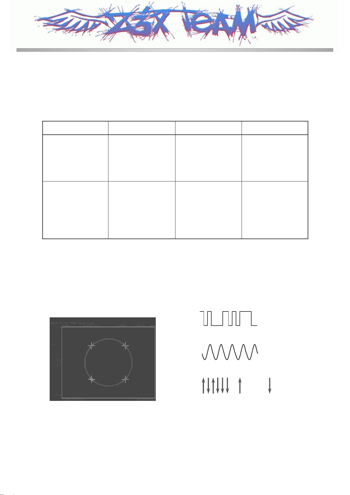
2.5 EDGE Air Interface - Modulation............. 9
3. Technical Brief............................... 11
3.1 Baseband Part Technical Brief ............ 11
3.1.1 BaseBand Components
(Main Component Side).............. 12
3.1.2 BaseBand Components
(Main Keypad Side) .................... 13
3.1.3 BaseBand Components (FPCB). 14
3.1.4 Digital Baseband(DBB) Processor 15
3.1.5 Analog Main Processor (ABB) .... 16
3.1.6 Memory....................................... 17
3.1.7 Power Management Section....... 17
3.1.8 MIDI ........................................... 18
3.1.9 CE500 Battery Icon Display........ 19
3.1.10 CE500 Battery Icon Display...... 20
3.1.11 Charging ................................... 20
3.1.12 KEY Back-light Illumination....... 21
3.1.13 SIM ........................................... 22
3.1.14 Keypad...................................... 23
3.2. RF Part Technical Brief ....................... 24
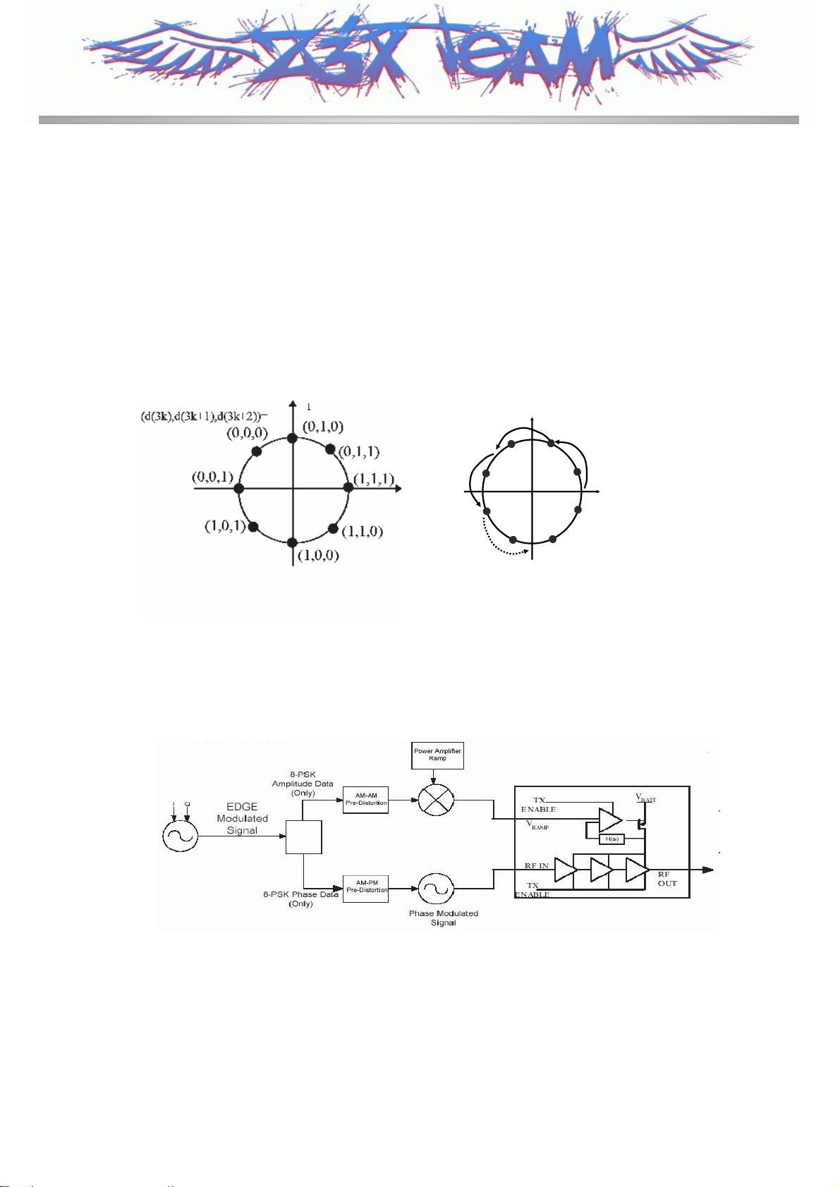
3.2.1 The Block Diagram of the RF Part
24
3.2.2 RF Part Components .................. 25
3.2.3 Tx / Rx Part Description.............. 26
3.2.4 Receiver Part Description ........... 29
3.2.5 Transmitter Part Description ....... 33
4. Troubleshooting............................ 36
4.1 Power On Trouble................................. 36
4.2 Charging Trouble .................................. 38
4.3 LCD Display Trouble............................. 40
4.4 Receiver Trouble................................... 42
4.5 Speaker Trouble ................................... 44
4.6 Microphone Trouble .............................. 46
4.7 Vibrator Trouble .................................... 48
4.8 Keypad Backlight Trouble (Main PCB) .. 50
4.9 Charging Indicator & MOD Key
Backlight Trouble .................................. 52
4.10 SIM Detect Trouble ............................. 54
4.11 Earphone Trouble ............................... 56
4.12 Transflash Trouble .............................. 60
4.13 RTC Trouble ....................................... 62
4.14 Camera Trouble .................................. 63
4.15 Camera Flash Trouble ........................ 65
4.16 RX Part Trouble Shooting ................... 67
4.17 TX Part Trouble Shooting .................. 75
5. DOWNLOAD .................................. 79
6. BLOCK DIAGRAM......................... 85
7. Circuit Diagram ............................. 87
8. pcb layout ..................................... 94
9. Calibration ..................................... 97
A. What is Calibration? ........................ 97
B. Calibration program .........................98
C. AGC ................................................ 99
D. APC................................................. 99
E. ADC................................................. 99
F. Setting ............................................. 99
G. Calibration Equipment Setup ........ 100
H. What is Standalone Test? ............. 101
I. Standalone Test Setup ................... 101
J. Tx Standalone Test........................ 102
K. Rx Standalone Test ...................... 103
L. Standalone Test Equipment Setup 104
10. EXPLODED VIEW &
REPLACEMENT PART LIST .... 105
10.1 EXPLODED VIEW ............................ 105
10.2 Replacement Parts
<Mechanic component>.................... 107
<Main component> ........................... 110
10.3 Accessory ......................................... 127
Table of Contents
Z3X-BOX.COM

1. Introduction
- 5 -
1.1. Purpose
This manual provides the information necessary to repair, calibration, description and download the
features of the CE500.
1.2. Regulatory Information
1.2.1. Security
Toll fraud, the unauthorized use of telecommunications system by an unauthorized part (for example,
persons other than your company’s employees, agents, subcontractors, or person working on your
company’s behalf) can result in substantial additional charges you’re your telecommunications
services. System users are responsible for the security of own system. There are may be risks of toll
fraud associated with your telecommunications system. System users are responsible for
programming and configuring the equipment to prevent unauthorized use. LGE does not warrant that
this product is immune from the above case but will prevent unauthorized use of common-carrier
telecommunication service of facilities accessed through or connected to it. LGE will not be
responsible for any charges that result from such unauthorized use.
1.2.2. Incidence of Harm
If a telephone company determines that the equipment provided to customer is faulty and possibly
causing harm or interruption in service to the telephone network, it should disconnect telephone
service until repair can be done. A telephone company may temporarily disconnect service as long as
repair is not done.
1.2.3. Changes in Service
A local telephone company may make changes in its communications facilities or procedure. If these
changes could reasonably be expected to affect the use of the CE500 or compatibility with the network,
the telephone company is required to give advanced written notice to the user, allowing the user to
take appropriate steps to maintain telephone service.
1.2.4. Maintenance Limitations
Maintenance limitations on the CE500 must be performed only by the LGE or its authorized agent.
The user may not make any changes and/or repairs expect as specifically noted in this manual.
Therefore, note that unauthorized alternations or repair may affect the regulatory status of the system
and may void any remaining warranty.
I. Introduction
Z3X-BOX.COM

1. Introduction
- 6 -
1.2.5. Notice of Radiated Emissions
The CE500 complies with rules regarding radiation and radio frequency emission as defined by local
regulatory agencies. In accordance with these agencies, you may be required to provide information
such as the following to the end user.
1.2.6. Pictures
The pictures in this manual are for illustrative purposes only; your actual hardware may look slightly
different.
1.2.7. Interference and Attenuation
An CE500 may interfere with sensitive laboratory equipment, medical equipment, etc. Interference
from unsuppressed engines or electric motors may cause problems.
1.2.8. Electrostatic Sensitive Devices
ATTENTION
Boards, which contain Electrostatic Sensitive Device (ESD), are indicated by the sign. Following
information is ESD handling: Service personnel should ground themselves by using a wrist strap when
exchange system boards.
When repairs are made to a system board, they should spread the floor with anti-static mat which is
also grounded. Use a suitable, grounded soldering iron. Keep sensitive parts in these protective
packages until these are used. When returning system boards or parts such as EEPROM to the
factory, use the protective package as described.
Z3X-BOX.COM

2. General Performance
- 7 -
2.1 H/W Feature
A. Hardware Feature
• Class: GPRS/ EDGE Class 10
• Radio: Triple Band (850/1800/1900)
• Camera: VGA 330K CMOS
• Display: Main : 1.86” 128x160, 65K TFT
Sub : 1.17” 96x96, 65K TFT
• Connectivity: IrDA, USB
• Sound: 64 Poly MIDI, MP3 Play
• Battery: 1000 mAh (min) Li-Ion
• Size / weight: 93.8 X 47.9 X 24.5 mm, 107g
B. Software Feature
• Music Player (MP3, AAC)
• MP3 Ringtone, 3D Surround Sound
• Graphic EQ
• E-mail Client, Sync ML(DS)
• Video Clip
• Instant Messaging, MMS
• WAP 2.0, JAVA 2.0,
• FR / EFR / HR / AMR
2.2 GPRS / EDGE Comparison
2. General Performance
Parameter GSM/GPRS EDGE
Carrier spacing 200 kHz 200 kHz
Frame length 4.6 ms frames 4.6 ms frames
Timeslots per carrier 8 8
Modulation GMSK 8-PSK (also GMSK)
Symbol rate 270 ksymbols/s 270 ksymbols/s
Modulation bit rate 270 kb/s 810 kb/s
Radio data rate per time slot 22.8 kb/s 69.2 kb/s
Max. user data rate per time slot 20 kb/s (CS4) 59.2 kb/s (MCS9)
Max user data rate-8 time slots 160 kb/s (182.4 kb/s) 473.6 kb/s (553.6 kb/s)
Link Quality Control (LQC) None LA and IR
Z3X-BOX.COM

2. General Performance
- 8 -
2.3 Modulation and Coding Rates for EDGE
• 8-PSK added for higher data rates
2.4 GSM Air Interface
• Uses 0.3GMSK modulation: 1 bit/symbol
• Constant envelope
• 200 kHz channel bandwidth
MCS Modulation Code Rate Bit Rate/Timeslot
MCS-1 0.53 8.8
MCS-2
GMSK
0.66 11.2
MCS-3 0.8 14.8
MCS-4 1 17.6
MCS-5 0.37 22.4
MCS-6 0.49 29.6
MCS-7 8-PSK 0.76 44.8
MCS-8 0.92 54.5
MCS-9 1 59.2
Data 270.833 kB/s
Frequency
+67.708 kHz
-67.708 kHz
Phase +90
-90
Z3X-BOX.COM

2. General Performance
- 9 -
2.5 EDGE Air Interface - Modulation
• 8-PSK modulation is used for high data rates
• Signal trajectory will pass through the origin
• High peak-to-average ratio
• 8-PSK constellation rotates 3 /8 radians per symbol period
• Rotation prevents zero crossings, reducing peak-to-average power
• Polar transmitter and Direct modulation transmitter Block diagram
Polar transmitter Block diagram
(1,1,1) t = 0 (symbols)
(1,1,1) t = 1
(1,1,1) t = 2
(1,1,1) t = 3
3/8 radians
...
Z3X-BOX.COM

2. General Performance
- 10 -
Direct modulation transmitter Block diagram
• Polar transmitter and Direct modulation transmitter comparison
• Polar and Direct modulation transmitter Comparison
TRF
TLF
VBAT
PA
(RF)
A(t)
(t)
TRF
TLF
VBAT
PA
(RF)
Vapc
A(t)+(t)
Polar transmitter Direct modulation transmitter
Polar Transmitter Direct modulation Transmitter
PA Nonlinear (saturated mode) Linear Susceptible
Stable against antenna VSWR to antenna VSWR (EVM,Spectrum)
Risk concerning in High delay in amplitude/phase path No
mass production AM/AM & AM/PM spread of PA
Z3X-BOX.COM

3. Technical Brief
- 11 -
3. Technical Brief
3.1 Baseband Part Technical Brief
Main LCD
Folder PBAMain PBA
DBB
(AD6532)
ABB
(AD6555)
Memory
(PD38F4050L0ZBQ0)
MIDI
(YMU783)
MIC I/O Connector
SIM
Battery
R
F
LCD
Connec
tor
Ear_Mic
F
P
C
B
Charging
Block
TA
Analog
S/W
Ear
jack
Data Cable,Ö
Multimedia
(MV8602)
Speaker
Vibrator
Camera
Camera
Flash LED
Receiver
Sub LCD
MP3 Play
Mode Key
TransFlash Card
IrDA
The Block Diagram of the Baseband Part
Z3X-BOX.COM

3. Technical Brief
- 12 -
3.1.1. BaseBand Components (Main Component Side)
J301
X701
S501
J201
CN501
U101
U502
U103
U207
U602
CN401
PAD501
U603
Camera KEY
SIDE KEY
U101 Analog Baseband Chipset(AD6555)
U103 Digital Baseband Chipset(AD6532)
U207 Memory (256M Flash x 64M PSRAM)
U602 Multimedia IC
CN501 IO Connector
J201 EAR Jack
U603 MIDI IC (64 Poly)
J301 SIM Connector
X701 VCTCXO (13MHz)
U502 Charge Pump
CN401 FPCB Connector (70pin)
S501 T-Flash Memory Connector
PAD501 Battery Connector
Z3X-BOX.COM

3. Technical Brief
- 16 -
3.1.5 Analog Main Processor (ABB)
GMSK
Modulator
TX
DAC
TX
DAC
SC
Filter
SC
Filter
Active
CT Filter
Active
CT Filter
8PSK
Modulator
Digital Filter
Digital Filter
RX
DAC
RX
DAC
SC
Filter
SC
Filter
PWM Output
Controller
PWM Output
Controller
PWM Output
Controller
Voltage
Reference
AUX
ADC
RAMP RAM
Ramp
DAC
SC
Filter
Active
CT Filter
AFC
DAC
Ringtone
Volume Controller
SC
Filter
SC
Filter
DAC
1
DAC
2
ADC
Analog
Switch
Analog
Switch
SC
Filter ADC
Control
Serial
Port
Baseband
Serial
Port
Audio
Serial
Port
PGA
Gain Pre Amp
Analo g Adde r
PGA
PGA
Analo g Adde r
PGA
Microphone Interface
SC
Filter
PGA
PGA
PGA
REFTXCM
BSIFS
BSDI
BSOFS
BSDO
CSFS
CSDI
CSDO
GPI
ASFS
ASDI
ASDO
BSDI
TXON
RXON
ASM
IP
MCLKEN
RESET
IN
QP
QN
VAPCDAC
AFCDAC
LIGHT1
LIGHT2
LIGHT3
LGND
REFBB
REFOUT
REFCHG
REF
TEMP1
TEMP2
AUXADC1
AUXADC2
AIN1P
AIN2P
BATTYPE
ISENSE
VBATSENSE
AIN3R
AIN3L
SPWR
AOUT 2P
AOUT 2N
SGND
AOUT 1P
AOUT 1N
AOUT 3L
AOUT 3R
AIN1P
AIN1N
AIN2P
AIN2N
MCLK
AD6555
Voiceband Baseband Codec
JTAG Interface
TCK TMS TDO TDI
Block diagram of the AD6555
Z3X-BOX.COM

3. Technical Brief
- 17 -
3.1.6 Memory
• 256 Mbit flash memory + 64Mbit PSRAM
• 16 bit parallel data bus
• ADD0 ~ ADD23.
• 2 Chip enables for Flash memory select.
• RF Calibration data and battery calibration data are also stored in Flash memory area.
3.1.7 Power Management Section
- VCORE : supplies Digital Baseband Processor
core and D6532 digital core (0.8V ~
105V, 300mA)
- VMEM : supplies external memory and the
interface to the external memory on
the digital baseband processor (1,8V
or 2.8V, 150mA)
- VEXT : supplies Radio digital interface and
high voltage interface (2.8V, 200mA)
- VSIM : supplies the SIM interface circuitry
on the digital processor and SIM
card (1.8V or 2.85V, 20mA)
- VRTC : supplies the Real-Time Clock
module (2.8 V, 20 •
µ
A)
- VABB : supplies the analog portions of the
AD6555
- VMIC : supplies the microphone interface
circuitry (2.5 V, 2 mA)
- VVCXO : supplies the voltage controlled
crystal oscillator ( 2.75 V, 10 mA)
- VBACK : supplies the Real-Time Clock module and charges the backup battery (1.8V or 2.8V, 50mA)
- VUSB : supplies the USB interface (3.3V, 15mA)
- VPLL : supplies the phased-lock loops
- VINT : supplies the AD6555 digital core and the interface to the AD6555 on the digital baseband processor
(1.8v, 80mA)
Z3X-BOX.COM

3. Technical Brief
- 19 -
3.1.9 CE500 Battery Icon Display
3.79V
3.72V
3.53V
25 % 25
%
25
%
3.45V
3.93V
25
%
3.62V
3.71V~3.62V
3.61V~3.53V
5 minutes available
at Tx level 5
blink
3.52V~3.45V
3.62V~3.45V
IDLE
blink
CALL
4.2V~3.93V 3.92V~3.79V 3.78V~3.72V
-After discharging the battery cell for CE500 , it is like the following figure.
-1000mAhLi-ionbattery , discharge current : 192.7mA(0.2C)
Z3X-BOX.COM

3. Technical Brief
- 20 -
3.1.10 CE500 Battery Icon Display
•Battery Bar Display
1) BAR 4 : Over 3.93 ±0.03V
2) BAR 4 →BAR 3 : 3.92 ±0.03V
3) BAR 3 →BAR 2 : 3.79 ±0.03V
4) BAR 2 →BAR 1 : 3.72 ±0.03V
5) BAR 1 →BAR 0 : 3.62 ±0.03V
6) BAR Blinking : 3.52 ±0.03V (Calling : 3.62 0.03V)
7) Power OFF : 3.45 ±0.03V
•Low battery Warning (Standby) : 3.520.03V , 1 time per 3mins.
(Talk) : 3.620.03V , 1 time per 1min.
3.1.11 Charging
• Charging method : CC-CV
• Charger detect voltage : 4.0V
• Charging time : about 2h
• Charging current : 480mA
• CV voltage : 4.2V
• Low battery alarm
- Idle : 3.52V
- Call : 3.62V
• Power-off voltage : 3.45V
• Charging temperature ADC range
- ~ -5°C : not charging operation.
- -5°C ~ 50°C: charging.
- 50°C ~ : not charging operation.
4.2V ~ 3.93V 3.92V ~ 3.79V 3.78V ~ 3.72V 3.71V ~ 3.62V 3.61V ~ 3.53V
Z3X-BOX.COM

3. Technical Brief
- 21 -
3.1.12 KEY Back-light Illumination
• KEYPAD Back-light Scheme.
NA
KEY BACKLIGHT
NA
LD304
R322 47
R338
100K
47R323
0R336
R321 47
LD307
LD310
1.5K
R337
R325
47
47
R326
LD302
LD313
LD311
R329 47
R335 0
LD309
VA314
AVL5M02-200
47R330
LD308
VA313
AVL5M02-200
47
LD301
R327
R320 47
R340
10
47R328
LD314
LD312
LD306
47R333
LD305
AVL5M02-200
VA312
R324 47
56
31
4
IMX9T110
Q302
2
LD303
47R334
47
R331
R332 47
10
R339
VBAT
LD315
KEY_BACKLIGHT
KEY Backlight (main PCB part)
Z3X-BOX.COM
Other manuals for CE500
5
Table of contents
Other LG Cell Phone manuals