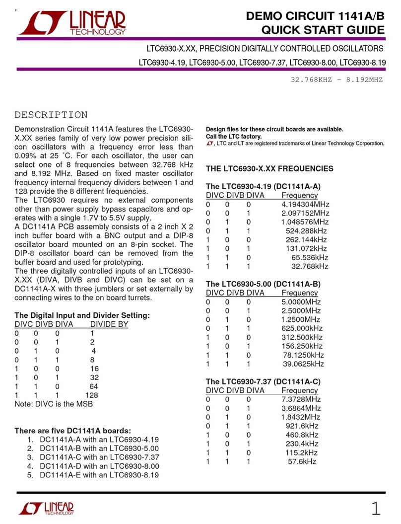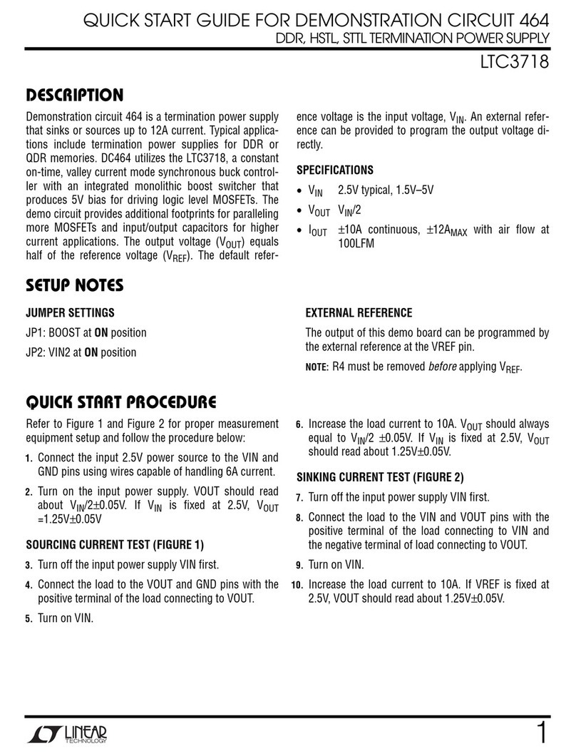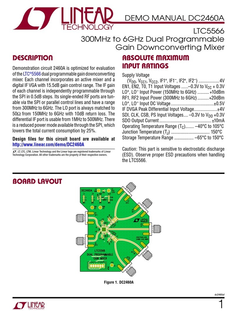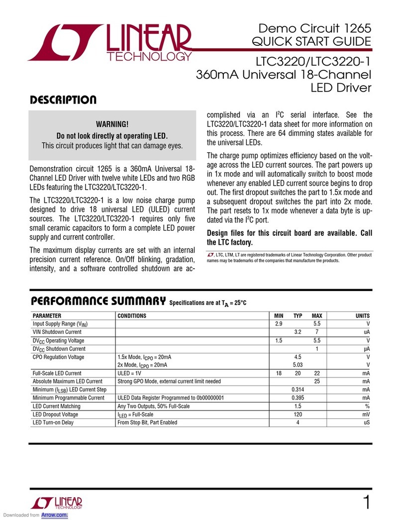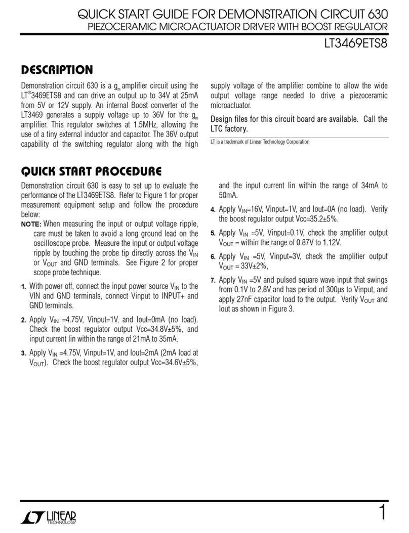
Figure 2. Measuring Input/Output Ripple
OPERATION
The LT3740 is a current-mode synchronous buck
controller that can accept input voltages as low as
2.2V, and as high as 22V, but still provides at least
7V for the MOSFET gate drives through an internal
boost regulator. It is equipped for No Rsense
TM
operation to maximize efficiency and features
three user selectable current limit ranges and a
flexible soft-start system capable of output track-
ing.
To close the current loop, the LT3740 reads the
switching current through the bottom MOSFET
“on” resistance. The chip features three user se-
lectable current limit thresholds to optimize effi-
ciency: 45mV, 75mV and 105mV. DC947 uses the
middle setting, but unpopulated pads are available
for selecting the other two settings.
In the interest of making the board able to handle a
wide variety of input and output voltage combina-
tions, DC947 does not use the No Rsense
TM
fea-
ture, but has been configured so that it is easy to
do so. This is accomplished by shorting out the
R1 sense resistor and moving the zero ohm resis-
tor at location R14 to location R13. Change R28
to 1 ohm. Other component changes unique to
the desired output voltage, input voltage range and
frequency compensation may be necessary.
DC947 is configured such that the bottom gate
drive power (BGDP) pin is connected directly to
the output of the on-chip boost regulator (BIAS)
through R32. This is what allows the circuit to pro-
vide sufficient power MOSFET gate drive when the
input is as low as 3V.
If the design is not required to operate at input
voltages below 7V, the BGDP pin can be tied to
Vin to reduce the loading on the boost converter
and thus save power. To do this, move the zero
ohm resistor at location R32 to R31 and add a 1uF
ceramic capacitor at location C25. Also, imple-
ment the UVLO circuit by removing R30 and popu-
lating the circuitry made up of D3, Q3, and R29.
The LT3740 has an active high, open collector
power good signal. On the demo board, it is pulled
up to the 1.8V output through a 100K resistor, and
can be conveniently read at TP6. Note that this
pull-up voltage may not be compatible with all volt-
age systems. Please refer to the data sheet for a
detailed description of the PGOOD signal.
A 0-0.8V external reference may be applied to the
LT3740 at TP5. This is used to over-ride the inter-
nal 0.8V reference, giving control of the DC947
output voltage to an external signal source. Use of
this function must first be enabled by setting JP1
(REFERENCE) to the EXTERNAL position. For
further details about the external reference func-
tion, please refer to the XREF function described
in the LT3740 data sheet.
JP2 (VOLTAGE_SS) and JP3 (CURRENT_SS)
must both be set to their respective ON positions
in order for the DC947 output to power up. If ei-
ther of these jumpers is set to the OFF position,
the output will not turn on. JP2 (VOLTAGE_SS) is
associated with the XREF input, while JP3
(CURRENT_SS) ties into the SHDN input. For
further details about the LT3740 soft-start opera-
tion, please refer to the data sheet.
On the DC947 demo board, the signals applied to
both of the soft-start inputs are generated by sim-
ple RC circuits. The RC time constant of the
CURRENT_SS soft-start is much longer than that
of the VOLTAGE_SS, so the CURRENT_SS will
