3
dc752af
DEMO MANUAL DC752A
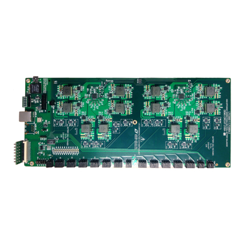
JUMPERS
JP8, JP9: Tie points for GND1 and GND2, respectively.
The default selection is TIE for both jumpers. This con-
nects all DAC grounds to the analog ground plane, and is
suitable for most applications that do not have large return
currents into the GND1 and GND2 turrets. Alternatively,
selecting REMOTE allows GND1 and GND2 to differ by as
much as ±300mV from analog ground.
JP1, JP2, JP4, JP6: Sense connections for DACA, DACB,
DACC, and DACD, respectively. Selecting TIE connects
OUTFx (output force) output directly to OUTSx (output
sense). Selecting REMOTE allows for remote sensing of
the output voltage. This also allows a power gain stage
such as the LT1970 to be added with no degradation of
accuracy.
JP3 (REF1): Voltage reference selection for DACA and
DACB, either 5V for the onboard LT1236 reference or
REMOTE if an external reference source is connected to
the REF1 turret post.
JP5 (REF2): Voltage reference selection for DACC and
DACD, either 5V for the onboard LT1236 reference or
REMOTE if an external reference source is connected to
the REF2 turret post.
JP10 (VOSA), JP12 (VOSB), JP11 (VOSC), JP13 (VOSD):
offset adjustment selection for DACA, DACB, DACC, and
DACD, respectively. If no offset adjustment is required,
select GND. Selecting ADJ connects the offset pin to the
associated 10-turn pot, allowing adjustment of the DAC’s
offset.
JP7: Select source for 5V VCC supply. Normally this should
be left in the REF position for lowest noise operation. The
REG position selects the 5V regulated supply from the
14-pin QuikEval connector. To apply an external supply,
remove JP7 completely.
ANALOG CONNECTIONS (TURRET POSTS)
OUTFA, OUTFB, OUTFC, OUTFD: DAC voltage outputs.
OUTSA, OUTSB, OUTSC, OUTSD: DAC feedback inputs.
The LTC2704 RFB inputs have a nominal 10k resistance,
so resistance between this point an the load or buffer
output must be kept low.
REF1,REF2:DAC Reference voltage. If theonboardLT1236
references are selected, the voltage may be measured at
these points. If a remote reference is selected, then an
external reference must be applied to these points.
REFM1, REFM2: Inverted reference output from the
LTC2704.Donotdrivethesepointswithanexternalsource.
POWER AND GROUND CONNECTIONS
Analog Power: The +15V, –15V, and GND turret posts
are the analog supplies for the internal DAC amplifiers.
These should be connected to a well regulated, low noise
power supply.
VCC:Connection to VCC. See schematic and description
for JP7.
Grounding: Separate power and signal grounds are pro-
vided. Signal ground is connected to the exposed ground
planes at the top and bottom edges of the board, and to
the two turrets labeled AGND. Use signal ground as the
reference point for measurements and connections to
external circuits. Any large currents drawn from the DAC
outputs should be returned to the power ground turret
closest to pin 1 on the 14-pin header. In this situation,
GND1 and GND2 can be used to sense the ground voltage
attheload,compensating for return resistance between the
load and power ground return. The maximum difference
in voltage between the load and power ground should be
less than 300mV.
HarDware setup
Downloaded from Arrow.com.Downloaded from Arrow.com.Downloaded from Arrow.com.

