Linx TRM-900-TT Instruction Manual

TT Series
Remote Control Transceiver
Data Guide

Table of Contents
1 Description
1 Features
2 Ordering Information
2 Electrical Specications
4 Absolute Maximum Ratings
4 Typical Performance Graphs
10 Pin Assignments
10 Pin Descriptions
12 Theory of Operation
13 Module Description
14 Basic Hardware Operation
16 Transceiver Operation
17 Transmit Operation
17 Receive Operation
18 The Pair Process
19 Permissions Mask
19 Acknowledgement
20 Mode Indicator
20 Reset to Factory Default
21 Using the RSSI Line
21 Using the LATCH_EN Line
22 Using the Low Power Features
22 Using the LVL_ADJ Line
24 The Command Data Interface
27 Frequency Hopping
28 Usage Guidelines for FCC Compliance
28 Additional Testing Requirements
29 Information to the user
30 Antenna Selection

––
1
Description
The TT Series transceiver is designed for
reliable bi-directional, long-range remote
control applications. It consists of a highly
optimized Frequency Hopping Spread
Spectrum (FHSS) RF transceiver and
integrated remote control transcoder. The
FHSS system allows higher power and,
therefore, longer range than narrowband radios. The TT Series transceiver
has obtained modular approval for the United States and Canada.
Eight status lines can be set up in any combination of inputs and outputs
for the transfer of button or contact states. A selectable acknowledgement
indicates that the transmission was successfully received. Operating in
the 902 to 928MHz frequency band, the module is capable of generating
+12.5dBm and achieves a typical sensitivity of -113dBm.
Primary settings are hardware-selectable, which eliminates the need for an
external microcontroller or other digital interface. For advanced features,
optional software configuration is provided by a UART interface; however,
no programming is required for basic operation.
Housed in a compact reflow-compatible SMD package, the transceiver
requires no external RF components except an antenna, which greatly
simplifies integration and lowers assembly costs.
Features
• FCC and Canada pre-certified
• Long range (1 mile line of sight)
• Low power consumption (19mA
RX, 35mA TX @ +12.5dBm)
• No programming required
• 8 status lines
• Bi-directional remote control
• No external RF components
required
• Selectable acknowledgements
• No production tuning required
• 232 possible addresses
• Serial interface for optional
software operation
TT Series
Remote Control Transceiver
Data Guide
Figure 1: Package Dimensions
Revised 3/7/13
0.131"
0.630"
1.150"
11
Model: TRM-900-TTModel: TRM-900-TT
Lot FX9nnTLot FX9nnT
FCC ID: OJMTRM900TTAFCC ID: OJMTRM900TTA
IC: 5840A-TRM900TTAIC: 5840A-TRM900TTA
A large-print version of this document is available at
www.linxtechnologies.com.
31 Product Labeling
31 FCC RF Exposure Statement
32 Typical Applications
34 Power Supply Requirements
34 Antenna Considerations
35 Helpful Application Notes from Linx
36 Interference Considerations
37 Pad Layout
37 Board Layout Guidelines
39 Microstrip Details
40 Production Guidelines
40 Hand Assembly
40 Automated Assembly
42 General Antenna Rules
44 Common Antenna Styles
46 Regulatory Considerations
Warning: This product incorporates numerous static-sensitive
components. Always wear an ESD wrist strap and observe proper ESD
handling procedures when working with this device. Failure to observe
this precaution may result in module damage or failure.

–– – –
23
TT Series Transceiver Specifications
Parameter Symbol Min. Typ. Max. Units Notes
Power Supply
Operating Voltage VCC 2.5 5.5 VDC
TX Supply Current lCCTX
At +12.5dBm 33.9 38.1 mA 1,2
At 0dBm 15.2 18.9 mA 1,2
RX Supply Current lCCRX 19.2 22.7 mA 1,2
Standby Current lSTD TBD mA 1,2
Power-Down Current lPDN 1.0 µA 1,2
RF Section
Operating Frequency Band FC902 928 MHz 3
Center Frequency Accuracy –5 +5 kHz 2
Number of Channels 25 3,10
Channel Spacing 500 kHz 3
Modulation Rate 45 kbps
Receiver Section
Spurious Emissions −62 dBm
Receiver Sensitivity -111 dBm 5
RSSI Dynamic Range 64 dB
Transmitter Section
Output Power PO−15.5 +12.5 dBm 6
Output Power Control
Range
28 dB
Harmonic Emissions PH−42 –36 dBc 7
Frequency Deviation ±70 kHz
Electrical Specications
Ordering Information
Part Number Description
TRM-900-TT 900MHz TT Series Remote Control Transceiver
MDEV-900-TT TT Series Master Development System
Figure 2: Ordering Information
TT Series Transceiver Specifications
Parameter Symbol Min. Typ. Max. Units Notes
Antenna Port
RF Impedance RI N 50 Ω
Environmental
Operating Temp. Range −40 +85 ºC
Storage Temp. Range −55 +125 ºC
Timing
Module Turn-On Time
Via VCC TBD TBD ms 4
Via POWER_DOWN TBD TBD ms 4
Via Standby TBD TBD ms 4
Serial Command Response
Factory Reset/Erase Table 560 ms 11
Write NV Parameter 8 38 ms 11
Write V/Read/Control 2 13 ms 11
IU to RU Status High 4 50 ms 10
Channel Dwell Time 12.3 12.7 ms
Interface Section
POWER_DOWN, ACK_EN
Logic Low VI L VCC*0.2 VDC
Logic High VI H VCC*0.8 VCC VDC
Input
Logic Low VI L 0.8 VDC
Logic Low VI L
Logic High VI H
Logic High VI H 2 5.5 VDC
Output
Logic Low VOL 0.6 VDC
Logic High VOH VCC–0.7 VCC VDC
Certifications
Modular Certifications FCC, Industry Canada
Transceivers are supplied in tubes of 18 pcs.
1. Measured at 3.3V VCC
2. Measured at 25ºC
3. Guaranteed by design
4. Characterized but not tested
5. BER=10–3
6. Into a 50-ohm load
7. PO=+12.5dBm (max output power)
8. 4.5V ≤VCC ≤5.5V
9. VCC ≤4.5V
10. No RF interference
11. Response time is from end of
command to start of response
Figure 3: Electrical Specifications

–– – –
45
Absolute Maximum Ratings
Supply Voltage Vcc −0.3 to +5.5 VDC
Any Input or Output Pin −0.3 to VCC + 0.3 VDC
RF Input 0 dBm
Operating Temperature −40 to +85 ºC
Storage Temperature −55 to +125 ºC
Exceeding any of the limits of this section may lead to permanent damage to the device.
Furthermore, extended operation at these maximum ratings may reduce the life of this
device.
Absolute Maximum Ratings
Figure 4: Absolute Maximum Ratings
Typical Performance Graphs
TX Output Power (dBm)
LVL_ADJ Resistance (kΩ)
-17
-12
-7
-2
3
8
13
0150 300450 600 750 900
Figure 6: TT Series Transceiver Output Power vs. LVL_ADJ Resistance
10
15
20
25
30
35
40
-20 -15 -10 -5 0510 15
Icc (mA)
TX Output Power (dBm)
-40°C
+25°C
+85°C
10
15
20
25
30
35
40
-20 -15 -10 -5 0510 15
Icc (mA)
TX Output Power (dBm)
-40°C
+25°C
+85°C
Figure 7: TT Series Transceiver Current Consumption vs. Transmitter Output Power at 3.3V
Figure 8: TT Series Transceiver Current Consumption vs. Transmitter Output Power at 5.5V
TX Vcc
TX Sx
TX MODE_IND
RX Sx
ABCDE FGH
RX MODE_IND
AB – TX Power up Response – <80ms
BC – RX Initial Response – 8 to 50ms with no interference
CD – Data Settle – 4 to 8us
EF – Data Update Delay During Active Session – 5 to 25ms
EG – Shutdown Duration – 25 to 342ms
GH – RX MODE_IND Drop – 6 to 8ms
VON
TT Series Transceiver Timings
Item Description Minimum Maximum
AB
TX Response from VCC or POWER_DOWN180ms
TX Response from Status line while IU in idle212ms
TX Response from Status line while IU / RU idle in RX31ms
BC RX Initial Response 8ms 50ms
CD Data Settle 4µs 8µs
EF Data Update Delay During Active Session 5ms 25ms
EG Shutdown Duration 25ms 342ms
GH RX MODE_IND Drop 6ms 8ms
Figure 5: TT Series Timings
1. From module off to VCC applied
2. The module is set as an IU only and is in idle pending status line activation
3. The module is set as an IU and RU and is idling in receive mode pending status line
activation or receipt of a valid packet.

–– – –
67
16
17
18
19
20
21
22
2.53.5 4.
55
.5
RX Icc (mA)
Supply Voltage (V)
-40°C
+25°C
+85°C
14
15
16
17
2.53.5 4.
55
.5
TX Icc (mA)
Supply Voltage (V)
-40°C
+25°C
+85°C
Figure 10: TT Series Transceiver TX Current Consumption vs. Supply Voltage at 0dBm
Figure 11: TT Series Transceiver RX Current Consumption vs. Supply Voltage
0
1
2
3
4
5
6
-30 -40 -50 -60 -70 -80 -90 -100 -110
RSSI Output Voltage (V)
RF Input Power Level (dBm)
2.5V Vcc
3.3V Vcc
5.5V Vcc
Figure 12: TT Series Transceiver RSSI Voltage vs. Input Power
Figure 9: TT Series Transceiver TX Current Consumption vs. Supply Voltage at +12.5dBm
32
33
34
35
36
37
2.53.5 4.
55
.5
TX Icc (mA)
Supply Voltage (V)
-40°C
+25°C
+85°C

–– – –
89

–– – –
10 11
Pin Assignments
GND
NC
GND GND
NC
NC
GND
NC
NC
NC
NC
NC
GND
NC
GND
ANTENNA
1
2
3
4
5
6
7
83
7
38
39
40
41
42
43
44
S0
S1
GND GND
PAIR
C1
ACK_OUT
C0
CMD_DATA_OUT
LATCH_EN
S2
S3
LVL_ADJ
RESET
ACK_EN
MODE_IND
9
10
11
12
13
14
15
16 29
30
31
32
33
34
35
36
GND
S7
S6 S5
VCC
POWER_DOWN
GND
S4
RSSI
GND
GND
CMD_DATA_IN
17
18
19
20
21
22
23
24
25
26
27
28
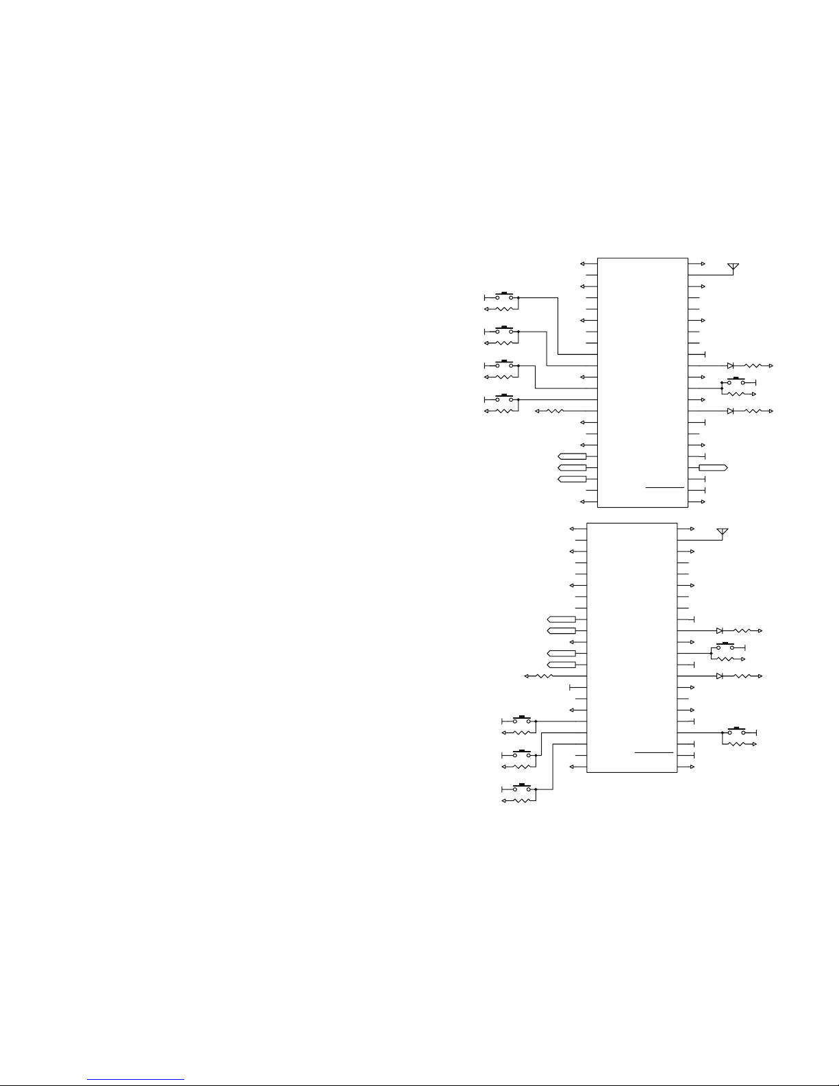
Figure 13: TT Series Transceiver Pin Assignments (Top View)
Pin Descriptions
Pin Number Name I/O Description
1, 3, 6, 11,
17, 22, 23,
28, 34, 39,
42, 44
GND — Ground
2, 4, 5, 7, 8,
37, 38, 40, 41 NC — No Electrical Connection. Do not connect
any traces to these lines.
9, 10, 12, 13,
18, 19, 20, 26 S0 - S7 I/O
Status Lines. Each line can be configured
as either an input to register button or
contact closures or as an output to control
application circuitry.
14 LVL_ADJ 1I
Level Adjust. This line sets the transmitter
output power level. Pull high or leave open
for the highest power; connect to GND
through a resistor to lower the power.
Pin Descriptions Continued
Pin Number Name I/O Description
15 LATCH_EN I
If this line is high, then the status line
outputs are latched (a received command
to activate a status line toggles the output
state). If this line is low, then the output lines
are momentary (active for as long as a valid
signal is received) and which are latched.
16 RESET I
Pull low to perform a soft reset of the
module. This line has an internal pull-up to
POWER_DOWN, may be left unconnected
21 RSSI O
Received Signal Strength Indicator. This line
outputs an analog voltage that increases
with the strength of the received signal. It is
updated once a second.
24 POWER_DOWN I
Power Down. Pulling this line low places the
module into a low-power state. The module
is not functional in this state. Pull high for
normal operation. Do not leave floating.
25 VCC — Supply Voltage
27 CMD_DATA_IN I Command Data In. Input line for the serial
interface commands
29 CMD_DATA_OUT O Command Data Out. Output line for the
serial interface commands
30, 32 C0 I
This line sets the input/output direction for
status lines S0-S3. When low, the lines are
outputs; when high they are inputs.
31 ACK_OUT O
This line goes high when the module
receives an acknowledgement message
from another module after sending a control
message.
32 C1 I
This line sets the input/output direction for
status lines S4-S7. When low, the lines are
outputs; when high they are inputs.
33 PAIR I
A high on this line initiates the Pair process,
which causes two units to accept each
other’s transmissions. It is also used with
a special sequence to reset the module to
factory default configuration
35 MODE_IND O
This line indicates module activity. It can
source enough current to drive a small
LED, causing it to flash. The duration of the
flashes indicates the module’s current state.
36 ACK_EN I
Pull this line high to enable the module to
send an acknowledgement message after a
valid control message has been received.
43 ANTENNA — 50-ohm RF Antenna Port
1. This line has an internal 100kΩpull-up resistor
Figure 14: TT Series Transceiver Pin Descriptions
Pin Descriptions

–– – –
12 13
Theory of Operation
The TT Series transceiver is a low-cost, high-performance synthesized
FSK transceiver. Its exceptional sensitivity results in outstanding range
performance. Figure 15 shows a block diagram for the module.
The TT Series transceiver is designed for operation in the 902 to 928MHz
frequency band. The RF synthesizer contains a VCO and a low-noise
fractional-N PLL. The VCO operates at twice the fundamental frequency
to reduce spurious emissions. The receive and transmit synthesizers
are integrated, enabling them to be automatically configured to achieve
optimum phase noise, modulation quality and settling time.
The transmitter output power is programmable from −15.5dBm to
+12.5dBm with automatic PA ramping to meet transient spurious
specifications. The ramping and frequency deviation are optimized to
deliver the highest performance over a wide range of data rates.
The receiver incorporates highly efficient low-noise amplifiers that provide
up to -113dBm sensitivity. Advanced interference blocking makes the
transceiver extremely robust when in the presence of interference.
A low-power onboard communications processor performs the radio
control and management functions. A control processor performs the
higher level functions and controls the serial and hardware interfaces.
This block also includes voltage translation to allow the internal circuits to
operate at a low voltage to conserve power while enabling the interface to
operate over the full external voltage. This prevents hardware damage and
communication errors due to voltage level differences.
While operation is recommended from 3.3V to 5.0V, the transceiver can
operate down to 2.5V.
RSSI/
LOGAMP
LNAFSK
DEMOD
CDR
AFC
AGC
PROCESSOR
26MHz
OSC
PA RAMP
PROFILE
PA
8-BIT
ADC
LOOP
FILTER
CHARGE
PUMP PFD
DIVIDER
Σ-Δ
MODULATOR
GAUSSIAN
FILTER
f
DEV
DIVIDER
LNA
ANTENNA
GPIO /
INTERFACE
LDO
VCC
PDN
INTERFACE /
VOLTAGE
TRANSLATION
Figure 15: TT Series Transceiver RF Section Block Diagram
Module Description
The TT Series Remote Control module is a completely integrated RF
transceiver and processor. It has two main modes of operation: hardware
and software. Hardware operation is basic and is suitable for applications
like keyfobs where no other processor, PC or interface is present. Software
operation is more advanced and allows for more features and functionality.
This guide focuses on hardware operation with some references to
software operation. Please see Reference Guide RG-00103: the TT Series
Command Data Interface for details on software operation.
The module has 8 status lines numbered S0 through S7. These can be set
as inputs for buttons or contacts or as outputs to drive application circuitry.
When S0 is taken high on one side S0 goes high on the other side, and so
forth. A line that is an input on one side needs to be set as an output on
the other side.
Since this module can act as both transmitter and receiver, terminology and
descriptions can get confusing. This guide uses the term Initiating Unit (IU)
to describe a module that is transmitting commands. Responding Unit (RU)
is used to describe a module that is receiving commands.
The transceiver uses a Frequency Hopping Spread Spectrum (FHSS)
algorithm. This allows for higher output power and longer range than
narrow-band systems while still maintaining regulatory compliance. All
aspects of managing the FHSS operations are automatically handled by the
module.
The TT Series has received modular certification for the FCC in the United
States and Industry Canada when used with an approved antenna. The
module may be placed in an end product without further transmitter
testing, though unintentional radiator testing may be required. Please see
the Usage Guidelines for FCC Compliance section for more details.

–– – –
14 15
Basic Hardware Operation
The following steps describe how to use the TT Series module with
hardware only. Basic application circuits that correspond to these steps are
shown in Figure 16.
1. Set the C0 and C1 lines opposite on both sides.
2. Press the PAIR button on both sides. The MODE_IND LED begins
flashing slowly to indicate that the module is searching for another
module.
3. Once the pairing is complete, the MODE_IND LED flashes quickly to
indicate that the pairing was successful.
4. The modules are now paired and ready for normal use.
5. Pressing a status line button on one module activates the
corresponding status line output on the second module.
6. Taking the ACK_EN line high on the RU causes the module to send an
acknowledgement to the IU. The ACK_OUT line on the IU goes high to
indicate that the acknowledgement has been received. Tying the line
to Vcc causes the module to send an acknowledgement as soon as a
command message is received.
This is suitable for basic remote control or command systems. No
programming is necessary for basic hardware operation. The following
sections describe the functions in more detail and the Typical Applications
section shows additional example schematics for using the modules.
The Command Data Interface section describes the more advanced
features that are available with the serial interface.
1
TRM-XXX-TT
NC
2
GND
3
NC
4
NC
5
GND
6
NC
7
S0
9
S1
10
GND
11
S7
18
S6
19
RSSI
21
GND
22 GND23
POWER_DOWN 24
VCC25
S5 26
CMD_DATA_IN27
S2
12
GND
17
S3
13
LVL_ADJ
14
LATCH_EN
15
RESET
16
NC
8
S4
20
GND
GND28
CMD_DATA_OUT29
C0 30
ACK_OUT31
C1 32
PAIR 33
GND34
MODE_IND 35
ACK_EN 36
NC 37
NC 38
GND39
NC 40
NC 41
GND42
ANTENNA 43
GND44
GND
GND
GND
GND
GND
GNDGND
GND
GND
GND
GND
GND
VCC
VCC
GND
100k
100k
100k
100k
GND
91k 1%
GND
GND
GND
GND
VCC
VCC
VCC
VCC
GND
S7
S6
S4
S5
VCC
GND
GND
GND
VCC
VCC
NC
2
GND
3
NC
4
NC
5
GND
6
NC
7
S0
9
S1
10
GND
11
S7
18
S6
19
RSSI
21
GND
22 GND23
POWER_DOWN24
VCC25
S5 26
CMD_DATA_IN 27
S2
12
GND
17
S3
13
LVL_ADJ
14
LATCH_EN
15
RESET
16
NC
8
S4
20
GND
1
GND28
CMD_DATA_OUT29
C0 30
ACK_OUT31
C1 32
PAIR 33
GND34
MODE_IND 35
ACK_EN36
NC 37
NC 38
GND39
NC 40
NC 41
GND42
ANTENNA 43
GND44
TRM-XXX-TT
GND
GND
GND
GND
GND
GNDGND
GND
GND
GND
GND
GND
VCC
VCC
GND
91k 1%
GND
S0
S1
S2
S3
VCC
GND
GND
100k
GND
VCC
100k
100k
100k
GND
GND
GND
GND
VCC
VCC
VCC
VCC
VCC
100k
VCC
VCC
VCC
1
TRM-XXX-TT
NC
2
GND
3
NC
4
NC
5
GND
6
NC
7
S0
9
S1
10
GND
11
S7
18
S6
19
RSSI
21
GND
22 GND23
POWER_DOWN 24
VCC25
S5 26
CMD_DATA_IN27
S2
12
GND
17
S3
13
LVL_ADJ
14
LATCH_EN
15
RESET
16
NC
8
S4
20
GND
GND28
CMD_DATA_OUT29
C0 30
ACK_OUT31
C1 32
PAIR 33
GND34
MODE_IND 35
ACK_EN 36
NC 37
NC 38
GND39
NC 40
NC 41
GND42
ANTENNA 43
GND44
GND
GND
GND
GND
GND
GNDGND
GND
GND
GND
GND
GND
VCC
VCC
GND
100k
100k
100k
100k
GND
91k 1%
GND
GND
GND
GND
VCC
VCC
VCC
VCC
GND
S7
S6
S4
S5
VCC
GND
GND
GND
VCC
VCC
NC
2
GND
3
NC
4
NC
5
GND
6
NC
7
S0
9
S1
10
GND
11
S7
18
S6
19
RSSI
21
GND
22 GND23
POWER_DOWN24
VCC25
S5 26
CMD_DATA_IN 27
S2
12
GND
17
S3
13
LVL_ADJ
14
LATCH_EN
15
RESET
16
NC
8
S4
20
GND
1
GND28
CMD_DATA_OUT29
C0 30
ACK_OUT31
C1 32
PAIR 33
GND34
MODE_IND 35
ACK_EN36
NC 37
NC 38
GND39
NC 40
NC 41
GND42
ANTENNA 43
GND44
TRM-XXX-TT
GND
GND
GND
GND
GND
GN
DG
ND
GND
GND
GND
GND
GND
VCC
VCC
GND
91k 1%
GND
S0
S1
S2
S3
VCC
GND
GND
100k
GND
VCC
100k
100k
100k
GND
GND
GND
GND
VCC
VCC
VCC
VCC
VCC
100k
VCC
VCC
VCC
Figure 16: TT Series Transceiver Basic Application Circuits for Bi-directional Remote Control

–– – –
16 17
Transceiver Operation
The transceiver has two modes of operation: Initiating Unit (IU) that
transmits control messages and Responding Unit (RU) that receives control
messages. If all of the status lines are set as inputs, then the module is set
as an IU only. The module stays in a low power sleep mode until a status
line goes high, starting the Transmit Operation.
If all of the status lines are set as outputs, then the module is set as an RU
only. It stays in Receive Operation looking for a valid transmission from a
paired IU.
A module with both input and output status lines can operate as an IU
and an RU. The module idles in Receive Operation until either a valid
transmission is received or a status line input goes high, initiating the
Transmit operation.
When an input goes high, the transceiver captures the logic state of each
of the status lines. All lines that are set as outputs are recorded as logic
0s in the message. The line states are placed into a packet along with the
local 32-bit address. The IU transmits the packets as it hops among 25 RF
channels.
An RU receives the packet and checks its Paired Module List to see if the
IU has been paired with the module and is authorized to control it. If the
IU’s address is not in the table, then the RU ignores the transmission. If
the address is in the table, then the RU calculates the channel hopping
pattern from the IU’s address and sets its status line outputs according to
the received packet. It then hops along with the IU and updates the states
of its outputs with every packet. Its outputs can be connected to external
circuitry that activates when the lines go high.
The RU can also send an acknowledgement back to the IU. Using the
serial interface the RU can include up to two bytes of custom data with
the acknowledgement, such as sensor data or battery voltage levels.
By default the module sends back a simple acknowledgement (ACK). It
sends an Acknowledge with Data (AWD) response when custom data is
programmed into the module.
Transmit Operation
Transmit Operation is entered when any of the status line inputs go high.
During Transmit Operation, the MODE_IND line is high. The module
repeatedly transmits control messages containing the local address and
the state of all status lines. Between transmissions the module listens for
acknowledgement messages. If an Acknowledge (ACK) or Acknowledge
with Data (AWD) message is received for the transmitted data, the
ACK_OUT line is asserted for 100ms. The ACK_OUT timing restarts on
each ACK or AWD packet that is received.
The transceiver sends control messages every 12.5ms as long as any
of the status line inputs is high, updating the status line states with
each packet. When all input lines are low, the module starts the shutoff
sequence.
During the shutoff sequence, the transmitter sends at least one packet with
all outputs off. It then continues to transmit data until the current channel
hopping cycle is complete, resulting in balanced channel use. If an input
line is asserted during the shutoff sequence, the transmitter cancels the
shutoff and extends the transmission sequence.
Receive Operation
During Receive Operation, the module waits for a valid control message
from an authorized transceiver. When a valid message is received, it locks
on to the hopping pattern of the transmitter and asserts the MODE_IND
line. It compares the received status line states to the Permission Mask for
the IU to see if the IU is authorized to activate the lines. The module sets
all authorized outputs to match the received states.
Only status line outputs are affected by received commands. Commands
to change an input line produce no result.
The RU then checks the state of the ACK_EN line and transmits an
acknowledgement packet if it is high. It looks for the next valid packet while
maintaining the frequency hopping timing. As long as an RU is receiving
valid commands from a paired IU, it will not respond to any other unit.
Once eight consecutive packets are missed, the RU is logically
disconnected from the IU and waits for the next valid packet from any IU.

–– – –
18 19
Permissions Mask
The TT Series Transceiver has a Permissions Mask that is used to
control which lines an IU is authorized to control. With most systems, if
a transmitter is associated with a receiver then it has full control over the
receiver. With the Permissions Mask, a transmitter can be granted authority
to control only certain receiver outputs. If an IU does not have the authority
to activate a certain line, then the RU does not set it.
As an example, a factory worker can be given a fob that only opens the
door to the factory floor while the CEO has a fob that can also open
the executive offices. The hardware in the fobs is the same, but the
permissions masks are set differently for each fob.
The Pair process always sets the Permission Mask to full access. The mask
can be changed through the serial interface.
Acknowledgement
A responding module is able to send an acknowledgement to the
transmitting module. This allows the initiating module to know that the
responding side received the command.
When the Responding Unit (RU) receives a valid Control Packet, it
checks the state of the ACK_EN line. If it is high the module sends an
Acknowledgement Packet.
If the Initiating Unit (IU) receives an Acknowledgement Packet that has
the same Address and Status Byte as in the Control Packet it originally
sent, then it pulls the ACK_OUT line high. A continuous stream of Control
Packets that triggers a continuous stream of Acknowledgement Packets
keeps the ACK_OUT line high.
Connecting the ACK_EN line to VCC causes the RU to transmit
Acknowledgement Packets as soon as it receives a valid Control Packet.
Alternately this line can be controlled by an external circuit that raises the
line when a specific action has taken place. This confirms to the IU that the
action took place and not just acknowledges receipt of the signal.
The Pair Process
The Pair process enables two transceivers to communicate with each
other. Each transceiver has a local 32-bit address that is transmitted with
every packet. If the address in the received packet is not in the RU’s Paired
Module List, then the transceiver does not respond. Adding devices to
the authorized list is accomplished through the Pair process or by a serial
command. Each module can be paired with up to 40 other modules.
The Pair process is initiated by taking the PAIR line high on both units to
be associated. Activation can either be a momentary pulse (less than
two seconds) or a sustained high input, which can be used to extend the
search and successful pairing display. With a momentary activation, the
search is terminated after 30 seconds. If Pairing is started with a sustained
high input, the search continues as long as the PAIR input is high.
When Pair is activated, the module displays the Pair Search sequence
on the MODE_IND line (Figure 17) and goes into a search mode where it
looks for another module that is also in search mode. It alternates between
transmit and receive, enabling one unit to find the other and respond.
Once bidirectional communication is established, the two units store each
other’s addresses in their Paired Module List with full Permissions Mask
and display the Pair Found sequence on their MODE_IND lines. The Pair
Found sequence is displayed for at least 3 seconds. If the PAIR input is
held high from the beginning of Pairing, the Pair Found display is shown for
as long as PAIR is high.
When Pairing is initiated, the module pairs with the first unit it finds that is
also in Pair Search. If multiple systems are being Paired in the same area,
such as in a production environment, then steps should be taken to ensure
that the correct units are paired with each other.
The Pair process can be cancelled by taking PAIR high a second time.
If the address table is full when the PAIR line is raised, the Pair Error
sequence is displayed on the MODE_IND line for 10 seconds and neither
of the Pairing units will store an address. In this case, the module should
either be reset to clear the address table or the serial interface can be used
to remove addresses.
If a paired unit is already in the Paired Module List, then no additional entry
is added though the existing entry’s Permissions Mask may be modified.

–– – –
20 21
Using the RSSI Line
The module’s Received Signal Strength Indicator (RSSI) line outputs a
voltage proportional to the incoming signal strength. The RSSI Voltage vs.
Input Power graph in the Typical Performance Graphs section shows the
relationship between the RSSI voltage and the incoming signal power. This
line has a high impedance so an external buffer may be required for some
applications.
The RSSI line updates once a second showing either the strength
of the packet received within the last second or the current channel
measurement. The formula to convert the RSSI voltage to power in dBm is:
PRX = (VRSSI / VCC) * 60 – 105
The RSSI output can be utilized during testing or even as a product feature
to assess interference and channel quality by looking at the RSSI level with
all intended transmitters shut off.
Using the LATCH_EN Line
The LATCH_EN line sets the outputs to either momentary operation or
latched operation. During momentary operation the outputs go high for as
long as control messages are received instructing the module to take the
lines high. As soon as the control messages stop, the outputs go low.
During latched operation, when a signal is received to make a particular
status line high, it will remain high until a separate activation is received to
make it go low. The transmission must stop and the module must time out
before it will register a second transmission and toggle the outputs.
When the LATCH_EN line is high, all of the outputs are latched. A serial
command is available to configure latching of individual lines.
Note: The RSSI levels and dynamic range vary from part to part. It is
also important to remember that the RSSI output indicates the strength
of any in-band RF energy and not necessarily just that from the intended
transmitter; therefore, it should be used only to qualify the presence and
level of a signal. Using RSSI to determine distance or data validity is not
recommended.
Mode Indicator
The Mode Indicator line (MODE_IND) provides feedback about the current
state of the module. This line switches at different rates depending on the
module’s current operation. When an LED is connected to this line it blinks,
providing a visual indication to the user. Figure 17 gives the definitions of
the MODE_IND timings.
Reset to Factory Default
The transceiver is reset to factory default by taking the Pair line high briefly
4 times, then holding Pair high for more than 3 seconds. Each brief interval
must be high 0.1 to 2 seconds and low 0.1 to 2 seconds. (1 second
nominal high / low cycle). The sequence helps prevent accidental resets.
Once the sequence is recognized the MODE_IND line blinks the Reset
Acknowledgement defined in Figure 17 until the PAIR line goes low. After
the input goes low, the configuration is initialized. Factory reset also clears
the Paired Module table but does not change the local address.
If the PAIR input timing doesn’t match the reset sequence timing, the
module reverts to normal operation without a reset or pairing.
MODE_IND Timing
Module Status Display
Transmit Mode Solid ON when transmitting packets.
Receive Mode Solid ON when receiving packets.
Pair Search ON for 100ms, OFF for 900ms while searching for another unit
during the Pair process
Pair Found
ON for 400ms, OFF for 100ms when the transceiver has been
Paired with another transceiver. This is displayed for at least 3
seconds.
Pair Error ON for 100ms, OFF for 100ms when the address table is full and
another unit cannot be added.
Remote Pair Error
ON for 100ms, OFF for 100ms, ON for 100ms OFF for 300ms
when the remote unit’s address table is full and a Pair cannot be
completed.
Pair Cancelled ON for 100ms, OFF for 200ms, ON for 100ms when the Pair
process is cancelled.
Reset
Acknowledgement
ON for 600ms, OFF for 100ms, ON for 200ms, OFF for 100ms,
ON for 200ms and OFF for 100ms when the reset sequence is
recognized.
Extended Pair
Completed
Solid ON when the pairing operation is completed and waiting for
the PAIR line to go low.
Figure 17: MODE_IND Timing

–– – –
22 23
Power Level vs. Resistor Value
Power
Level
PO
(dBm)
1%
Resistor
Value
Power
Level
PO
(dBm)
1%
Resistor
Value
Power
Level
PO
(dBm)
1%
Resistor
value
57 12.2 Open 38 3.4 154k 19 −5.4 44.2k
56 12.1 750k 37 3.1 143k 18 −5.7 41.2k
55 12.1 649k 36 2.7 133k 17 −6.1 37.4k
54 11.8 576k 35 2.1 127k 16 −6.7 34.8k
53 11.8 510k 34 1.6 118k 15 −7.0 32.4k
52 9.5 453k 33 1.1 111k 14 −7.5 29.4k
51 9.7 412k 32 0.8 105k 13 −7.9 26.7k
50 8.9 347k 31 0.3 97.6k 12 −8.3 24.3k
49 8.3 340k 30 −0.1 91k 11 −8.8 22k
48 8.0 316k 29 −0.6 86.6k 10 −9.3 19.6k
47 7.4 287k 28 −0.9 80.6k 9 −9.1 17.4k
46 6.9 267k 27 −1.4 76.8k 8 −9.6 15.4k
45 6.7 243k 26 −1.8 71.5k 7 −10.2 13.3k
44 6.3 226k 25 −2.3 66.5k 6 −10.8 11.3k
43 5.8 210k 24 −2.8 62k 5 −11.5 9.53k
42 5.3 200k 23 −3.2 57.6k 4 −12.2 7.5k
41 4.8 182k 22 −3.7 54.9k 3 −13.0 5.76k
40 4.3 174k 21 −4.3 51k 2 −13.9 4.02k
39 4.0 165k 20 −4.8 47k 1 −14.5 2.32k
0 −15.7 750
Figure 18: Power Level vs. Resistor Value
Using the Low Power Features
The Power Down (POWER_DOWN) line can be used to completely power
down the transceiver module without the need for an external switch.
This line allows easy control of the transceiver power state from external
components, such as a microcontroller. The module is not functional while
in power down mode.
Using the LVL_ADJ Line
The Level Adjust (LVL_ADJ) line allows the transceiver’s output power to be
easily adjusted for range control or lower power consumption. This is done
by placing a resistor to ground on LVL_ADJ to form a voltage divider with
an internal 100kΩresistor. When the transceiver powers up, the voltage on
this line is measured and the output power level is set accordingly. When
LVL_ADJ is connected to VCC or floating, the output power and current
consumption are the highest. When connected to ground, the output
power and current are the lowest. The power is digitally controlled in 58
steps providing approximately 0.5dB per step. See the Typical Performance
Graphs section (Figure 6) for a graph of the output power vs. LVL_ADJ
resistance.
Even in designs where attenuation is not anticipated, it is a good idea to
place resistor pads connected to
LVL_ADJ and ground so that it can be used if needed. Figure 18 shows
the 1% tolerance resistor value that is needed to set each power level and
gives the approximate output power for each level. The output power levels
are approximate and may vary part-to-part.
Warning: The LVL_ADJ line uses a resistor divider to create a voltage
that determines the output power. Any additional current sourcing or
sinking can change this voltage and result in a different power level. The
power level should be checked to confirm that it is set as expected.
Warning: Pulling any of the module inputs high while in Power Down
can partially activate the module, increasing current consumption
and potentially placing it into an indeterminate state that could lead
to unpredictable operation. Pull all inputs low before pulling POWER_
DOWN low to prevent this issue. Lines that may be hardwired (for
example, the ACK_EN line) can be connected to the POWER_DOWN
line so that they are lowered when POWER_DOWN is lowered.

–– – –
24 25
The Command Data Interface
The TT Series transceiver has a serial Command Data Interface (CDI)
that offers the option to configure and control the transceiver through
software instead of through hardware. This interface consists of a standard
UART with a serial command set. This allows for fewer connections in
applications controlled by a microcontroller as well as for more control and
advanced features than can be offered through hardware pins alone.
The serial port uses the CMD_DATA_IN and CMD_DATA_OUT lines as a
UART. An automatic baud rate detection system allows the interface to run
at a variable data rate from 9.6kbps to 57.6kbps.
The Command Data Interface has two sets of operators. One is a set
of commands that performs specific tasks and the other is a set of
parameters that are for module configuration and status reporting. These
are shown in Figure 19.
TT Series Transceiver Command Data Interface Reference Guide has full
details on each command. Some key features available with the serial
interface are:
• Configure the module through software instead of setting the hardware
lines.
• Change the output power, providing the ability to lower power
consumption when signal levels are good and extend battery life.
• Individually set which status lines are inputs and outputs.
• Individually set status line outputs to operate as momentary or latched.
• Add or remove specific paired devices.
• Individually set Permission Masks that prevent certain paired devices
from activating certain status line outputs.
• Change the module’s local address for production or tracking purposes
or to replace a lost or broken product.
• Put the module into a low power state to conserve battery power.
• Receive the entire control message serially instead of needing to
monitor individual status lines. Get the IU address for logging access
attempts.
• Receive control messages from unpaired modules, allowing for
expansion of the system beyond the maximum of 40 paired units.
Access control and address validation can be undertaken by an
external processor or PC with more memory than the module.
• Serially configure and control acknowledge messages.
• Send and receive 2 bytes (16 bits) of custom data with each command
message and acknowledge message.
• Serially initiate transmission of control messages instead of triggering
the status line inputs.
• Set interrupts to notify an external processor when specific events
occur, such as receiving a control message.
• Read out the RSSI value for the last received packet and the current
ambient RF level.
The serial interface offers a great deal of flexibility for use more complicated
designs. Please see Reference Guide RG-00103: the TT Series Command
Data Interface for details on the CDI. A list of the serial commands is shown
in Figure 19 for reference.

–– – –
26 27
Command Data Interface Commands and Parameters
Command Description
Read Read the current value in volatile memory. If there is no volatile
value, then the non-volatile value is returned.
Write Write a new value to volatile memory.
Read NV Read the value in non-volatile memory.
Program Program a new value to non-volatile memory.
Set Default
Configuration Set all configuration items to their factory default values.
Erase All Addresses Erase all paired addresses from memory.
Transmit Control Data Transmit a control message.
Transmit ACK Transmit an acknowledgement for received data.
Transmit AWD Transmit an Acknowledge With Data (AWD) response with two
bytes of custom data.
Parameter Description
Device Name NULL-terminated string of up to 16 characters that identifies the
module. Read only.
Firmware Version 2 byte firmware version. Read only.
Serial Number 4 byte factory-set serial number. Read only.
Local Address The module’s 32-bit local address.
Status Line I/O Mask Status lines direction (1 = Inputs, 0 = Outputs), LSB = S0, used
when enabled by Control Source
Latch Mask Latching enable for output lines, LSB = S0, used when enabled
by Control Source
TX Power Level TX output power, signed nominal dBm, used when enabled by
Control Source
Control Source Configures the control options.
Message Select Select message types to capture for serial readout
Paired Module
Descriptor
Sets the index number, address and permissions mask of paired
modules.
I/O Lines Read the current state of the status and control lines.
RSSI Read the RSSI of the last packet received and ambient level.
Read only.
LADJ Read the voltage on the LVL_ADJ line. Read only.
Module Status Read the operating status of the module.
Captured Receive
Packet Read the last received packet. Read only.
Interrupt Mask Sets the mask for events to generate a break on CMD_DATA_
OUT.
Event Flags Event flags that are used with the Interrupt Mask.
Figure 19: TT Series Transceiver Command Data Interface Commands and Parameters
Frequency Hopping
The module incorporates a Frequency Hopping Spread Spectrum (FHSS)
algorithm. This provides immunity from narrow-band interference as well as
meets regulatory requirements for higher output power, resulting in longer
range.
The module uses 25 RF channels as shown in Figure 20.
Each channel has a timeslot of 12.5ms before the module hops to the next
channel. This equal spacing allows a receiver to hop to the next channel
at the correct time even if a packet is missed. Up to seven consecutive
packets can be missed without losing synchronization.
The hopping pattern is determined from the transmitter’s address. Each
sequence uses all 25 channels, but in different orders. Once a transmission
starts, the module continues through a complete cycle. If the input line
is taken low in the middle of a cycle, the module continues transmitting
through the end of the cycle to ensure balanced use of all channels.
Frequency hopping has several advantages over single channel operation.
Hopping systems are allowed a higher transmitter output power, which
results in longer range and better performance within that range. Since
the transmission is moving among multiple channels, interference on one
channel causes loss on that channel but does not corrupt the entire link.
This improves the reliability of the system.
Channel Frequencies
Channel
Number
Frequency Channel
Number
Frequency Channel
Number
Frequency
1 902.62 10 907.12 18 911.12
2 903.12 11 907.62 19 911.62
3 903.62 12 908.12 20 912.12
4 904.12 13 908.62 21 912.62
5 904.62 14 909.12 22 913.12
6 905.12 15 909.62 23 913.62
7 905.62 16 910.12 24 914.12
8 906.12 17 910.62 25 914.62
9 906.62
Figure 20: TT Series Transceiver RF Channel Frequencies

–– – –
28 29
Usage Guidelines for FCC Compliance
The TT Series module is provided with an FCC and Industry Canada
Modular Certification. This certification shows that the module meets the
requirements of FCC Part 15 and Industry Canada license-exempt RSS
standards for an intentional radiator. The integrator does not need to
conduct any further testing under these rules provided that the following
guidelines are met:
• An approved antenna must be directly coupled to the module’s U.FL
connector through an approved coaxial extension cable.
• Alternate antennas can be used, but may require the integrator to
perform certification testing.
• The module must not be modified in any way. Coupling of external
circuitry must not bypass the provided connectors.
• End product must be externally labeled with “Contains FCC ID:
OJMTRM900TTA / IC: 5840A-TRM900TTA”.
• The end product’s user’s manual must contain an FCC statement
equivalent to that listed on page 29 of this data guide.
• The antenna used for this transceiver must not be co-located or
operating in conjunction with any other antenna or transmitter.
• The integrator must not provide any information to the end-user on
how to install or remove the module from the end-product.
The integrator is required to perform unintentional radiator testing on the
final product per FCC sections 15.107 and 15.109 and IC RSS-GEN.
Any changes or modifications not expressly approved by Linx Technologies
could void the user’s authority to operate the equipment.
Additional Testing Requirements
The modules have been tested for compliance as an intentional radiator,
but the integrator is required to perform unintentional radiator testing
on the final product per FCC sections 15.107 and 15.109 and Industry
Canada license-exempt RSS standards. Additional product-specific testing
might be required. Please contact the FCC or Industry Canada regarding
regulatory requirements for the application. Ultimately is it the integrator’s
responsibility to show that their product complies with the regulations
applicable to their product.
Information to the user
The following information must be included in the product’s user manual.
FCC / IC NOTICES
This product contains FCC ID: OJMTRM900TTA / IC: 5840A-TRM900TTA
This device complies with Part 15 of the FCC rules and Industry Canada
license-exempt RSS standards. Operation of this device is subject to the
following two conditions:
1. This device may not cause harmful interference, and
2. this device must accept any interference received, including interference that
may cause undesired operation.
This equipment has been tested and found to comply with the limits for a Class
B digital device, pursuant to Part 15 of the FCC Rules. These limits are designed
to provide reasonable protection against harmful interference in a residential
installation. This equipment generates, uses and can radiate radio frequency
energy and, if not installed and used in accordance with the instructions,
may cause harmful interference to radio communications. However, there is
no guarantee that interference will not occur in a particular installation. If this
equipment does cause harmful interference to radio or television reception,
which can be determined by turning the equipment off and on, the user is
encouraged to try to correct the interference by one or more of the following
measures:
• Reorient or relocate the receiving antenna.
• Increase the separation between the equipment and receiver.
• Connect the equipment into an outlet on a circuit different from that to which
the receiver is connected.
• Consult the dealer or an experienced radio/TV technician for help.
Any modifications could void the user’s authority to operate the equipment.
Le présent appareil est conforme aux CNR d’Industrie Canada applicables
aux appareils radio exempts de licence. L’exploitation est autorisée aux deux
conditions suivantes:
1. l’appareil ne doit pas produire de brouillage, et
2. ’utilisateur de l’appareil doit accepter tout brouillage radioélectrique subi,
même si le brouillage est susceptible d’en compromettre le fonctionnement.

–– – –
30 31
Product Labeling
The end product must be labeled to meet the FCC and IC product label
requirements. It must have the below or similar text:
Contains FCC ID: OJMTRM900TTA / IC: 5840A-TRM900TTA
The label must be permanently affixed to the product and readily visible to
the user. ‘‘Permanently affixed’’ means that the label is etched, engraved,
stamped, silkscreened, indelibly printed, or otherwise permanently marked
on a permanently attached part of the equipment or on a nameplate of
metal, plastic, or other material fastened to the equipment by welding,
riveting, or a permanent adhesive. The label must be designed to last
the expected lifetime of the equipment in the environment in which the
equipment may be operated and must not be readily detachable.
FCC RF Exposure Statement
To satisfy RF exposure requirements, this device and its antenna must
operate with a separation distance of at least 20cm from all persons and
must not be co-located or operating in conjunction with any other antenna
or transmitter.
Antenna Selection
Under FCC and Industry Canada regulations, this radio transmitter may
only operate using an antenna of a type and maximum (or lesser) gain
approved for the transmitter by the FCC and Industry Canada. To reduce
potential radio interference to other users, the antenna type and its gain
should be so chosen that the equivalent isotropically radiated power
(e.i.r.p.) is not more than that necessary for successful communication.
The TRM-900-TT radio transmitter has been approved by the FCC and
Industry Canada to operate with the antenna types listed in Figure 21 with
the maximum permissible gain and required antenna impedance for each
antenna type indicated. Antenna types not included in this list, having a
gain greater than the maximum gain indicated for that type, are strictly
prohibited for use with this device.
Conformément à la réglementation d’Industrie Canada, le présent émetteur
radio peut fonctionner avec une antenne d’un type et d’un gain maximal
(ou inférieur) approuvé pour l’émetteur par Industrie Canada. Dans le but
de réduire les risques de brouillage radioélectrique à l’intention des autres
utilisateurs, il faut choisir le type d’antenne et son gain de sorte que la
puissance isotrope rayonnée équivalente (p.i.r.e.) ne dépasse pas l’intensité
nécessaire à l’établissement d’une communication satisfaisante.
Le présent émetteur radio (TRM-900-TT) a été approuvé par Industrie
Canada pour fonctionner avec les types d’antenne énumérés la Figure 21
et ayant un gain admissible maximal et l’impédance requise pour chaque
type d’antenne. Les types d’antenne non inclus dans cette liste, ou dont le
gain est supérieur au gain maximal indiqué, sont strictement interdits pour
l’exploitation de l’émetteur.
Antennas / Antennes
Linx Part Number
Référence Linx Type Gain Impedance
Impédance
ANT-916-CW-QW ¼ Wave Whip 1.84dBi 50Ω
ANT-916-PW-LP ¼ Wave Whip 2.44dBi 50Ω
ANT-916-SP Planar 1.35dBi 50Ω
ANT-916-WRT-RPS ½ Wave Dipole Helical 1.83dBi 50Ω
ANT-916-CHP ¼ Wave Whip 1.34dBi 50Ω
ANT-916-CW-HW ½ Wave Dipole Helical 1.83dBi 50Ω
Cable Assemblies / Assemblages de Câbles
Linx Part Number
Référence Linx Description
CSI-RSFB-300-UFMR* RP-SMA Bulkhead to U.FL with 300mm cable
CSI-RSFE-300-UFMR* RP-SMA External Mount Bulkhead to U.FL with 300mm cable
* Also available in 100mm and 200mm cable length
Figure 21: TT Series Approved Antennas

–– – –
32 33
In this example, C0 is low and C1 is high, so S0 - S3 are outputs and S4
- S7 are inputs. This is inverted from the circuit in Figure 22 making it the
matching device.
In this circuit, the Command Data Interface is connected to a
microcontroller for using some of the advanced features.
The microcontroller controls the state of the ACK_EN line. it can receive
a command, perform an action and then take the line high to send
Acknowledgement packets. This lets the user on the other end know that
the action took place and not just that the command was received.
Typical Applications
Figure 22 and Figure 23 show circuits using the TT Series transceiver.
In this example, C0 is high and C1 is low, so S0 - S3 are inputs and S4
- S7 are outputs. The inputs are connected to buttons that pull the lines
high and weak pull-down resistors to keep the lines from floating when
the buttons are not pressed. The outputs would be connected to external
application circuitry.
LATCH_EN is low, so the outputs are momentary.
The Command Data Interface is not used in this design, so CMD_DATA_IN
is tied high and CMD_DATA_OUT is not connected.
ACK_OUT and MODE_IND are connected to LEDs to provide visual
indication to the user.
PAIR is connected to a button and pull-down resistor to initiate the Pair
Process when the button is pressed.
ACK_EN is tied high so the module sends acknowledgements as soon as it
receives a control message.
1
TRM-XXX-TT
NC
2
GND
3
NC
4
NC
5
GND
6
NC
7
S0
9
S1
10
GND
11
S7
18
S6
19
RSSI
21
GND
22 GND23
POWER_DOWN 24
VCC25
S5 26
CMD_DATA_IN27
S2
12
GND
17
S3
13
LVL_ADJ
14
LATCH_EN
15
RESET
16
NC
8
S4
20
GND
GND28
CMD_DATA_OUT29
C0 30
ACK_OUT31
C1 32
PAIR 33
GND34
MODE_IND 35
ACK_EN 36
NC 37
NC 38
GND39
NC 40
NC 41
GND42
ANTENNA 43
GND44
GND
GND
GND
GND
GND
GNDGND
GND
GND
GND
GND
GND
VCC
VCC
GND
100k
100k
100k
100k
GND
91k 1%
GND
GND
GND
GND
VCC
VCC
VCC
VCC
GND
S7
S6
S4
S5
VCC
GND
GND
GND
VCC
VCC
NC
2
GND
3
NC
4
NC
5
GND
6
NC
7
S0
9
S1
10
GND
11
S7
18
S6
19
RSSI
21
GND
22 GND23
POWER_DOWN24
VCC25
S5 26
CMD_DATA_IN 27
S2
12
GND
17
S3
13
LVL_ADJ
14
LATCH_EN
15
RESET
16
NC
8
S4
20
GND
1
GND28
CMD_DATA_OUT29
C0 30
ACK_OUT31
C1 32
PAIR 33
GND34
MODE_IND 35
ACK_EN36
NC 37
NC 38
GND39
NC 40
NC 41
GND42
ANTENNA 43
GND44
TRM-XXX-TT
GND
GND
GND
GND
GND
GNDGND
GND
GND
GND
GND
GND
VCC
VCC
GND
91k 1%
GND
S0
S1
S2
S3
VCC
GND
GND
100k
GND
VCC
100k
100k
100k
GND
GND
GND
GND
VCC
VCC
VCC
VCC
VCC
100k
µ
VCC
RX
TX
GPIO
Figure 22: TT Series Transceiver Basic Application Circuit
1
TRM-XXX-TT
NC
2
GND
3
NC
4
NC
5
GND
6
NC
7
S0
9
S1
10
GND
11
S7
18
S6
19
RSSI
21
GND
22 GND23
POWER_DOWN 24
VCC25
S5 26
CMD_DATA_IN27
S2
12
GND
17
S3
13
LVL_ADJ
14
LATCH_EN
15
RESET
16
NC
8
S4
20
GND
GND28
CMD_DATA_OUT29
C0 30
ACK_OUT31
C1 32
PAIR 33
GND34
MODE_IND 35
ACK_EN 36
NC 37
NC 38
GND39
NC 40
NC 41
GND42
ANTENNA 43
GND44
GND
GND
GND
GND
GND
GNDGND
GND
GND
GND
GND
GND
VCC
VCC
GND
100k
100k
100k
100k
GND
91k 1%
GND
GND
GND
GND
VCC
VCC
VCC
VCC
GND
S7
S6
S4
S5
VCC
GND
GND
GND
VCC
VCC
NC
2
GND
3
NC
4
NC
5
GND
6
NC
7
S0
9
S1
10
GND
11
S7
18
S6
19
RSSI
21
GND
22 GND23
POWER_DOWN24
VCC25
S5 26
CMD_DATA_IN 27
S2
12
GND
17
S3
13
LVL_ADJ
14
LATCH_EN
15
RESET
16
NC
8
S4
20
GND
1
GND28
CMD_DATA_OUT29
C0 30
ACK_OUT31
C1 32
PAIR 33
GND34
MODE_IND 35
ACK_EN36
NC 37
NC 38
GND39
NC 40
NC 41
GND42
ANTENNA 43
GND44
TRM-XXX-TT
GND
GND
GND
GND
GND
GNDGND
GND
GND
GND
GND
GND
VCC
VCC
GND
91k 1%
GND
S0
S1
S2
S3
VCC
GND
GND
100k
GND
VCC
100k
100k
100k
GND
GND
GND
GND
VCC
VCC
VCC
VCC
VCC
100k
µ
VCC
RX
TX
GPIO
Figure 23: TT Series Transceiver Typical Application Circuit with External Microprocessor

–– – –
34 35
The transceiver includes a U.FL connector as well as a line for the
antenna connection. This offers the designer a great deal of flexibility in
antenna selection and location within the end product. Linx offers cable
assemblies with a U.FL connector on one end and several types of
standard and FCC-compliant reverse-polarity connectors on the other end.
Alternatively, the designer may wish to use the pin and route the antenna to
a PCB mount connector or even a printed loop trace antenna. This gives
the designer the greatest ability to optimize performance and cost within
the design.
Helpful Application Notes from Linx
It is not the intention of this manual to address in depth many of the issues
that should be considered to ensure that the modules function correctly
and deliver the maximum possible performance. We recommend reading
the application notes listed in Figure 26 which address in depth key areas
of RF design and application of Linx products. These applications notes
are available online at www.linxtechnologies.com or by contacting the Linx
literature department.
Power Supply Requirements
The transceiver incorporates a precision
low-dropout regulator which allows operation
over a wide input voltage range. Despite this
regulator, it is still important to provide a supply
that is free of noise. Power supply noise can
significantly affect the module’s performance, so
providing a clean power supply for the module
should be a high priority during design.
A 10Ωresistor in series with the supply followed by a 10µF tantalum
capacitor from Vcc to ground helps in cases where the quality of supply
power is poor (Figure 24). This filter should be placed close to the module’s
supply lines. These values may need to be adjusted depending on the
noise present on the supply line.
Antenna Considerations
The choice of antennas is a
critical and often overlooked
design consideration. The range,
performance and legality of an RF
link are critically dependent upon the
antenna. While adequate antenna
performance can often be obtained
by trial and error methods, antenna
design and matching is a complex
task. Professionally designed antennas such as those from Linx (Figure
25) help ensure maximum performance and FCC and other regulatory
compliance.
Linx transmitter modules typically have an output power that is higher
than the legal limits. This allows the designer to use an inefficient antenna
such as a loop trace or helical to meet size, cost or cosmetic requirements
and still achieve full legal output power for maximum range. If an efficient
antenna is used, then some attenuation of the output power will likely be
needed. This can easily be accomplished by using the LVL_ADJ line.
It is usually best to utilize a basic quarter-wave whip until your prototype
product is operating satisfactorily. Other antennas can then be evaluated
based on the cost, size and cosmetic requirements of the product.
Additional details are in Application Note AN-00500.
+
10Ω
10µF
Vcc IN
Vcc TO
MODULE
Figure 24: Supply Filter
Figure 25: Linx Antennas
Note: Either the connector or the line can be used for the antenna, but
not both at the same time.
Helpful Application Note Titles
Note Number Note Title
AN-00100 RF 101: Information for the RF Challenged
AN-00126 Considerations for Operation Within the 902–928MHz Band
AN-00130 Modulation Techniques for Low-Cost RF Data Links
AN-00140 The FCC Road: Part 15 from Concept to Approval
AN-00500 Antennas: Design, Application, Performance
AN-00501 Understanding Antenna Specifications and Operation
RG-00103 TT Series Transceiver Command Data Interface Reference Guide
Figure 26: Helpful Application Note Titles
This manual suits for next models
1
Table of contents
Other Linx Transceiver manuals

Linx
Linx HumRC User manual

Linx
Linx HumDT Series User manual

Linx
Linx HUM-A-900-PRO-UFL Instruction Manual

Linx
Linx TRM-315-LT Instruction Manual

Linx
Linx NT Series Instruction Manual

Linx
Linx TT Series Instruction Manual

Linx
Linx NT Series User manual

Linx
Linx HumPRO Series Instruction Manual

Linx
Linx HumPRO Series User manual