manuals.online logo
Brands
  1. Home
  2. •
  3. Brands
  4. •
  5. Marantz
  6. •
  7. Tuner
  8. •
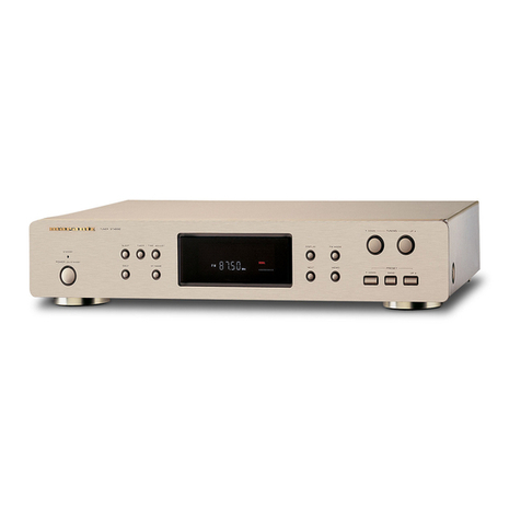
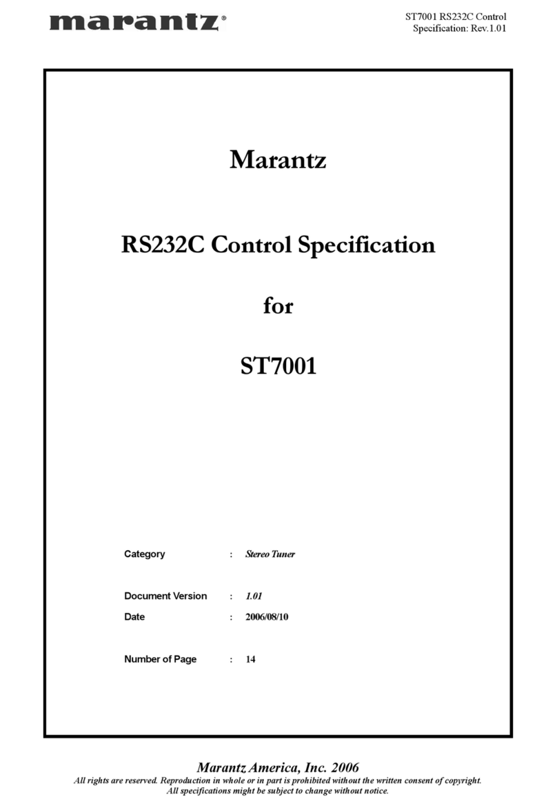
  9. Marantz ST-54 User manual

Marantz ST-54 User manual

v4l
I
frome
4
=“,
=
Life
model
ST
MARANTZ
DESIGN
AND
SERVICE
|
Using
superior
design
and
selected
high
grade
components,
MARANTZ
company
has
created
the
|
ultimate
in
stereo
sound.
,
Only
original
MARANTZ
parts
can
insure
that
your
i
MARANTZ
product
will
continue
to
perform
to
the
i
specifications
for
which
it
is
famous.
:
Parts
for
your
MARANTZ
equipment
are
generally
|
available
to
our
National
Marantz
Subsidiary
or
Agent.
|
ORDERING
PARTS:
Parts
can
be
ordered
either
by
mail
or
by
telex.
In
both
cases,
correct
part
number
has
to
be
specified.
If
you
order
by
mail,
fulfil
MARANTZ
order
forms.
The
following
information
must
be
supplied
to
eliminate
delays
in
processing
your
order:
.
Complete
address
.
Complete
part
numbers
and
quanties
required
.
Description
of
parts
TECHNICAL
ASSISTANCE
Should
you
require
any
other
technical
support,
do
not
hesitate
to
contact
the
Technical
Department
of
P.M.A.
MARANTZ
INTERNATIONAL
Quality
&
Service
Dept.
80,
Rue
des
Deux
Gares,
B-1070
Brussels
Belgium
Phone:
02/525.70.22
or
525.70.23
Telefax:
02/525.6160
Telex:
23550
OR
61511
(PHEMB)
routing:
BELDMZT
a
.
Way
of
shipment
oak
oan
—
and
void.
PARTS
ORDERING
AUSTRIA
HORNYPHON
Vertriebsgesellschaft
GmbH
Wienerbergstrasse
1
A
1101
Wien
Austria
Telex:
132.332
AUSTRALIA
MARANTZ
AUSTRALIA
PTY.,
Ltd.
19
Chard
Road
Brookvale,
NSW
2100
|
Australia
Telex:
24121
!
:
BELGIUM
;
SVD
DIVISION
MARANTZ
_Industrialaan
1
|1720
Groot-Bijgaarden
;
Belgium
|
Telex:
24466
|
CHILE
|
MARANTZ
|
DIVISION
OF
PHILIPS
S.A.
|
AV.
Santa
Maria,
0760
|
Casilla
2687
|
Santiago
Telex:
240.239
|
DENMARK
|
MARANTZ
,
DIVISION
OF
PHILIPS
SERVICE
A/S
:
Prags
Boulevard
80
Postbox
1919
|
DK-2300
Kebenhavn
S
+
Denmark
|
Telex:
31201
|
All
of
the
above
locations
are
fully
equipped
to
take
care
of
your
total
service
needs.
Because
various
countries
have
,
differing
configuration
requirements,
it
is
necessary
that
you
contact
the
service
facility
in
your
particular
country.
In
.
Model
number
for
which
part
is
required
Parts
may
be
ordered
at
the
following
addresses:
FINLAND
MARANTZ
DIVISION
OF
OY
PHILIPS
Ab
Kaivokatu
8
00100
Helsinki
Finland
Telex:
124811
FRANCE
MARANTZ
FRANCE
4
Rue
Bernard
Palissy
92600
Asniéres
France
Telex:
611651
GERMANY
MARANTZ
GERMANY
GmbH.
Max-Planck-Strasse
22
6072
Dreieich
1
Germany
Telex:
529821
THE
NETHERLANDS
Etpro
b.v.
De
Limiet
3
4131
NR
Vianen
The
Netherlands
Telex:
47679
NORWAY
MARANTZ.
DIVISION
OF
PHILIPS
A/S
Sandstuveien
40
Oslo
6
Norway
Telex:
72640
.
Signature:
any
order
form
or
telex
must
be
signed
otherwise
such
part
order
will
be
considered
as
null
GREAT
BRITAIN
MARANTZ
AUDIO
U.K.
Ltd
Unit
15/16
Saxon
Way
Industrial
Estate
Moor
Lane
Harmondsworth
UB7
OLW
Great
Britain
Telex:
935196
GREECE
SHERTON
ELECTRONICS
S.A.
P.O.Box
21025
Hippocratus
Street
188
Athens
11471
Greece
Telex:
216.795
JAPAN
MARANTZ
JAPAN,
Inc.
35-1,
7-chome,
Sagamiono
Sagamihara-shi,
Kanagawa
Japan
KUWAIT
AL
ALAMIAH
ELECTRONICS
Ussama
Building
Fahd
al
Saleem
Street
’
P.O.Box
23781
Safat-Kuwait
Telex:
22694
ITALY
MARANTZ
ITALIANA
S.P.A.
Via
Chiese,
74
20126
Milano
ttaly
SAUDI
ARABIA
AL
ALAMIAH
ELECTRONICS
P.O.Box
5954
University
Street
Riyadh
11432
Saudi
Arabia
Telex:
201530
SOUTH
AFRICA
MARANTZ
DIVISION
OF
PHILIPS
S.A.
Rainer
House
Ove
Street,
10
Doornfontein
Johannesburg
Telex:
483.456
SPAIN
PHONO
S.A.
Ignacio
Iglesias
10
Badalona
(Barcelona)
Spain
Telex:
59355
SWEDEN
MARANTZ
DIVISION
OF
PHILIPS
Foérsaljning
AB
Tegeluddsvagen
1
S-115
84
Stockhoim
Sweden
Telex:
14060
.
SWITZERLAND
DYNAVOX
ELECTRONICS
Route
de
Villars
105
1701
Fribourg
Switzerland
Telex:
942377
TURKEY
DOGRUOL
Ltd.
I.M.C.
6
Blok
N°6310
Unkapani
Istanbul
Turkey
®
Telex:
22085
MALTA
CACHIA
&
GALEA
Republic
Street,
68D
Valetta
Telex:
1682
U.S.A.
MARANTZ
COMPANY,
Inc.
National
Service
Department
P.O.Box
577
Chatsworth,
CA
91311
U.S.A.
ss
‘the
event
that
there
is
no
service
location
listed
for
your
country,
please,
contact
the
nearest
facility
for
the
necessary
In
case
of
difficulties,
do
not
hesitate
to
contact
the
Technical
Department
at
abovementioned
address.
assistance.
teenth
Sten
TABLE
OF
CONTENTS
SECTION
PAGE
1:
(PW
BOARDS
36200
8
pete)
ticins
pect
eae
tes
Gm
es
Gee
ee
a.
Qo
so
ae
en
ais
1
2.
TEST
EQUIPMENT
REQUIRED
FOR
SERVICING
..............
b
aust
ba
eae
a
2
3.
TUNER
ALIGNMENT
PROCEDURES
...........
0...
0...
ccc
ec
ee
eee
eee
een
n
nena
2
4.
TEST
POINT
AND
ALIGNMENT
POINTS
.............0
2000...
cee
cc
ee
eee
ee ee
teens
4
5.
CIRCUIT
‘DESCRIPTION:
6.
co.
-o.c8s
ethan
onde
deida
S
eee
nd
tied:
wolntwane
Sede
oe
ns
5
5.1
uPD1712CU-529
(0501)
FOR
AM/FM
TUNER...
..
..
oc
ee
ee
tte
tee
enna
5
5.2:
OUTLINE.OF
FUNCTIONS
iers.g.c55
ecade
6oe
oie
trate,
Shenae,
Rh
gee
aire
ie
veer
e
weil
Bao
b
leer
wi
aha
Oa
eNews
6
5.3
KEY
MATRIX
CONFIGURATION
...
0.0.0...
cc
ee
ee ee
eee
ee
tween
eee
eneeenae
6
5.4
DESCRIPTION
OF
KEY
MATRIX
........
2.0.
cc
cece
ee
eee
eee
ee
ee
eee
ete
ee
ene
7
5.5
STATIC
DRIVER
FOR
FREQUENCY
DISPLAY
TC9180N
(QRO1)
...
2...
0...
0
cee
eee
eee
te
ees
8
5.6
ELECTRODE
CONNECTION
(VRO1)
.......
ee
ee
ee
eee
te
eee
tee
e
nen
ee
9
6:
VOLTAGE
‘CONVERSION...
2.::8eS
a;
e068
eee
Os
Se
eee
ee
heel
eee
ei
Po
Pad
ed
9
7;
‘(BEOCK:
DIAGRAM!
vecwik
Siece
Sis
ta
en
deals
sheeeo
aha
Re
Oa
Rie
hae
ESE
10
8.
COMPONENT
LOCATIONS
......
ce
ccc
eee
een
nee
e
eee
eenaeueawe
11
8.1
Preset
Switch
Assembly
(PTOO)
Component
Locations
........
0.0.0
cee
eee
ce
eee
eee
nee
eee
11
8.2
Display
Assembly
(PROO)
Component
Locations
.........
000.
eee
eee
tee
tense
eens
11
8.3
IF
Band
Assembly
(PU00)
Component
Locations
......
0.0.0...
0c
eee
ee
ee
ee
eee
ete
teen
11
8.4
Power/Mode
Switch
Assembly
(PSO0)
Component
Locations
........0..
00
cee
eee
eee
ee
eae
ene
11
8.5
Mode
Lamp
Assembly
(PY00)
Component
Locations
...
0.0.0...
cece
eee
ete
teens
12
8.6
Power
Transf.
Assembly
(PPOO)
Component
Locations
..
0.0.0.0...
0c
ccc
eee
ee
ee
ee
ee
eee
etna
12
8.7
Tuner
Assembly
(P100)
Component
Locations..........;:.
esa
eed
a
der
Buena
wee
w a
ee
Cue
ab
6
Beetle.
12
9.
EXPLODED
VIEW
AND
PARTS
LIST
..........
00000
cece
ccc
ceee
ste
eceeeeeeeeees
14
10:-
EE
EGERICAL.
PARTS
-LIST
2
iii
cine
adc
vuimcda
ad
Ooo
nerd
Aaiate
elated
aig
lnce face
aeewhd
tend
17
11.
TECHNICAL
SPECIFICATIONS
..
2.0.0...
ccc
cc
ccc
cc
cee
eee
eee
n
eee
nennas
21
12.
SCHEMATIC
DIAGRAM
.....
0...
ccc
ee
eet
ee
nee
reece
ee
nee
nteeneeees
22
aa
a
aR
a
a
a
a
|
How
to
use
this
service
manual
e
The
“Common
parts’”
which
Marantz
Japan,
Inc.
has
established
are
eliminated
from
this
service
manual.
©
These
“Common
parts”
are
applied
to
all
models
in
the
service
manuals
arranged
and
issued
by
MJi.
©
To
indicate
clearly
the
common
parts
in
the
schematic
diagram,
a
line
is
drawn
above
or
under
the
Ref.
Desig.
No.
of
applicable
parts.
¢
"Common
parts”
can
be
supplied
from
the
Marantz
service
center
as
ever.
in
case
of
ordering,
please
establish
the
parts
number
of
12
N/C’S
following
the
procedure
mentioned
in
this
service
manual
"How
to
establish
the
parts
number
for
common
parts”.
1)
Please
correctly
write
the
parts
number
of
12
N/C’S
following
the
rule.
TERK
ESS
RS
TS
RE
RE
EK
ER
ES
ER
EE
ER SR
ERK
ER
EK
CER
ER
ER
ER
ER
ER
RE
Se
eee
eee
RC
ERR
ee
aa
ee
ey
Oa
a
a
a
a
ae
MZ
1532
MZ
1533
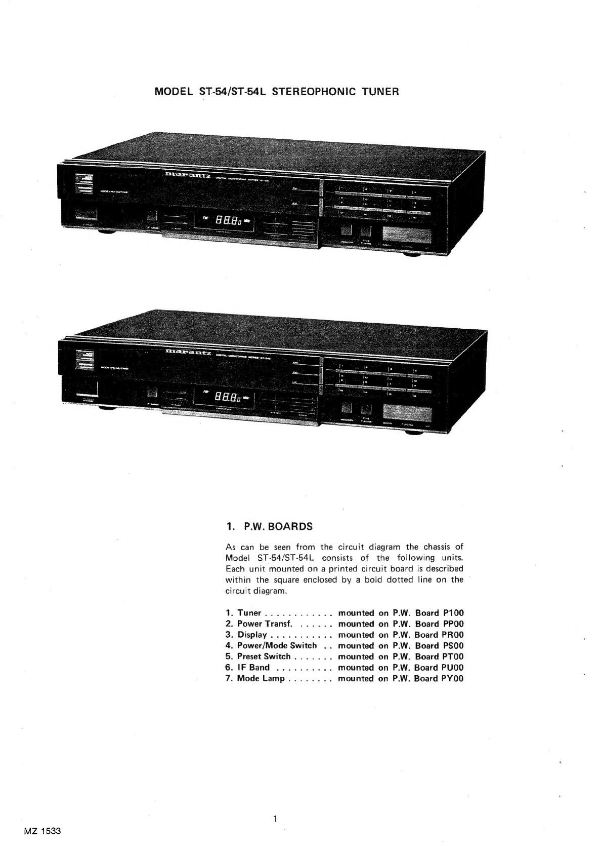
MODEL
ST-54/ST-54L
STEREOPHONIC
TUNER
1.
P.W.
BOARDS
As
can
be
seen
from
the
circuit
diagram
the
chassis
of
Model
ST-54/ST-54L
consists
of
the
following
units.
Each
unit
mounted
on
a
printed
circuit
board
is
described
within
the
square
enclosed
by
a
bold
dotted
line
on
the
©
circuit
diagram.
1.
Tuner
............
mounted
on
2.
Power
Transf.
......
mounted
on
3.
Display
...........
mounted
on
4.
Power/Mode
Switch
..
mounted
on
5.
Preset
Switch.
......
mounted
on
6.
IF
Band
..........
mounted
on
7.
Mode
Lamp........
mounted
on
1
P.W.
PW.
PW.
P.W.
P.W.
P.W.
P.W.
Board
P100
Board
PPO0O
Board
PROO
Board
PSOO
Board
PTOO
Board
PUOO
Board
PYOO
2.
TEST
EQUIPMENT
REQUIRED
FOR
SERVICING
Item
Use
AM
Signal
Generator
Signal
source
for
AM
alignment
——
Test
Loop
+
Use
with
AM
signal
generator
FM
Signal
Generator
Signal
source
for
FM
alignment
1
MPX
Signal
Generator
Distortion
Analyzer
;
Audio
Oscillator
Stereo
separation
alignment
and
trouble
shooting
Distortion
measurements
Sinewave
and
squarewave
signal
source
ee
r
AC
VTVM
Voltage
measurements
(AC)
Oscilloscope
Waveform
analysis
and
trouble
shooting
and
ASO
alignment
~~
Frequency
Counter
MPX
oscillator
adjustment
(VCO)
ame
a
Eee
Tester
Trouble
shooting
Voltage
measurements
(DC)
DC
VTVM
AC
Wattmeter
Line
Voltmeter
Variable
Autotransformer
(0
3.
TUNER
ALIGNMENT
PROCEDURES
~
140V
AC,
10A)
Monitors
primary
power
to
tuner
Monitors
potential
of
primary
power
to
tuner
Adjusts
level
of
primary
power
to
tuner
A
dummy
resistor
of
47
kohms
must
be
connected
across
the
tuner
output
terminals
before
alignment.
FM
Alignment
Procedures
(Function
switch
in
the
“FM
position,
MODE/FM
MUTING
Switch
in
the
MONAURAL/MUTING
OFF
position.)
1.
FM
RF
Alignment
(IF
BAND
switch
in
the
“WIDE”
position.)
=
Ste
Signal
Source
Signal
Indicator
Ir
Set
the
Digital
P
Connection
Frequency
Connection
Readout
Frequency
FM
signal
generator
to
FM
antenna
terminal
(300
ohm)
San
ce
aeetea
VTVM
to
Lor
R
FRONT
END
IFT
(L9)for
Leh
98.00
MHz
chnnel
output
98.00
MHz
maximum
output
and
level
so
that
some
noise
:
(3102)
:
aximumourpue
can
be
observed
on
the
minimum
distortion.
upper
and
lower
side
of
the
output
waveform.
FM
signal
generator
1
mV
output
to
FM
antenna
“O”’
center
meter
terminal
(300
ohm)
through
or
DC
current
meter
L202
core
so
that
2
matching
network
98.00
MHz
in
100
wA
range
98.00
MHz
the
meter
indicates
its
Modulation
Level
between
center
or
may
read
“O’’.
WHE
75
kHz
DEV.
(J100
1,
2}
DIN
40kHz
DEV.
output
to
FM
antenna
3
matching
network
Modulation
Level
\HE
75
kHz
DEV.
DIN
40kHz
DEV.
output
to
FM
antenna
terminal
(300
ohm)
thr
matching
network.
FM
signal
generator
1
mV
terminal
(300
ohm)
through
FM
signal
generator
1
mV
‘ough
aoe
98.00
MHz
98.00
MHz
“O"
center
meter
or
DC
current
meter
L203
(Primary)
core
so
in
100
vA
range
98.00
MHz
that
the
meter
indicates
its
between
center
or
may
read
O"’’.
(J200
1,
2)
ee
Distortion
meter
to.
Lor
R
channel
output
98.00
MHz
(J102)
L203
(Secondary)
core
for
minimum
distortion.
MZ
1534
2.
FMIF
Alignment
Procedures
(Function
switch
in
the
‘“FM’’
position,
MODE/FM
MUTING
switch
in
the
AUTO
STEREO/MUTING
ON
position.)
1F
BAND
switch
in
the
“WIDE”
position.
Signal
Source
Signal
Indicator
Set
the
Digital
Connection
Frequency
Connection
Readout
Frequency
R334
so
that
FM
signal
generator
.
7
Frequency
counter
1
mV
output
modulated
No
modulation
to
300
1,
2)
Frequency
may
precisely
by
MPX
signal
generator
read
76,000
kHz
(V.C.O)
inal
a
choinscan
Stereo
left
VTVM
to
left
(1,000
Hz)
channel
output
98.00
MHz
matching
network
Modulation
Level
(J102
L
ch)
FRONT
END
IFT
(L9)
IHF
67.5kHz+9%
Pilot
DEV.
:
for
minimum
DIN
40kHz
+8%
Pilot
DEV.
Stereo
right
VTVM
to
right
distortion
channel
output
{1,000
Hz)
(J102
R
ch)
Indicator
Connection
Splat
Siaied
Stereo
ieft
VTVM
to
left
by
MPX
signal
generator
(1,000
Hz}
channel!
output
to
FM
antenna
terminal
(J102
L
ch)
1300
ohin!
shrouey
aan
iis
matching
networ
3
Modulation
Level
Stereo
right
Abra
bs
IHF
67.5kHz+9%Pilot
DEV.|
(1,000
Hz)
phennel
eu
DIN
40kHz
+8%
Pilot
DEV.
RF
generator
to
FM
antennaterminais
through
:
matching
network
ice
ae
ae
(300
ohms,
balanced)
with
al
.
EL
a
the
RF
signal
level
set
so
98.00
MHz
ley
pe
ak
LED
that
the
signal
strength
(ort
Le
4
points.
LED
may
Sight
4
points
at
IF
band
switch
“Wide”
3.
Muting
Level
Alignment
(Function
switch
in
the
““FM’’
position,
MODE/FM
MUTING
switch
in
the
AUTO
STEREO/MUTING
ON
position.)
IF
BAND
switch
in
the
“WIDE”
position.
Signai
indicator
Set
the
Digital
Frequency
Connection
Readout
Frequency
—
4.
Multiplex
Alignment
Procedures
(Function
switch
in
the
“FM”
position,
MODE/FM
MUTING
switch
in
the
AUTO
STEREO/MUTING
ON
position.)
FM
signal
generator
VTVM
to
right
Set
the
Digital
Readout
Frequency
1
mV
output
modulated
Stereo
Seft
channel
output
si
1,000
:
CEM
antenna
vecminal
ea
(J102
R
ch)
IF
BAND
WIDE
326
(300
ohm)
through
98.00
MHz
bese
Ww
ieee
‘or
matching
network
e
ee
in
Modulation
Level
Stereo
right
VTVM
to
left
oth
channels.
tHE
67.5kHz+9%
Pilot
DEV
(1,000
Hz)
channel
output
L201
for
minimum
distortion
Signai
Source
Connection
FM
signal
generator
12.5
wV
output
to
FM
antenna
terminal
through
matching
network
(300
ohm,
balanced)
VTVM
to
Lor
R
channel
output
(J102)
Adjust
R233
until
output
is
developed.
y
DIN
40kHz
+8%
Pilot
DEV.
(J102
L
ch)
Repeat
steps
1
and
2.
RF
generator
to
FM
antenna
terminals
through
VTVM
to
right
R330
so
that
mimimum
matching
network
Pilot
only
and
left
channel
output
should
be
the
(300
ohms,
balanced)
output
(J102)
same
in
both
channels
with
1
mV
FM
stereo
signal.
MZ
1535
AM
Alignment
Procedures
(Function
switch
in
the
“AM”
position.)
1.
AMIE
Alignment
Step
Signal
Source
Signal
Indicator
Set the
Digital
Connection
Frequency
Connection
Readout
Frequency
Sweep
generator
to
Oscilloscope
to
1
AM
Antenna
Terminal.
450
kHz
marker
J300
(2,
3)
2.
AMRF
Alignment
a
Signal
Source
Signal
Connection
Frequency
Indicator
Connection
Set the
Digital
Readout
Frequency
Apply
the
signal
to
the
AM
loop
antenna
from
the
AM
signal
generator
using
the
test
loop.
600
kHz
600
kHz
VTVM
to
Lor
R
channel!
output
(J102)
1,400
kHz
1,400
kHz
Repeat
steps
1
and
2.
Step
Signal
Source
Signal
Indicator
Set
the
Digital
Connection
Frequency
Connection
Readout
Frequency
Apply
the
signal
to
the
173
kHz
173
kHz
AM
loop
antenna
from
the
VTVM
to
L
or
R
RF
generator
using
the
nena
output
test
loop.
272
kHz
272
kHz
Repeat
steps
1
and
2
as
necessary
to
obtain
maximum
sensitivity.
4.
AM
Signal
Alignment
(Function
switch
in
the
“AM”
position)
Signal
Source
Signal
Indicator
Set
the
Digital
Connection
Frequency
Connection
Readout
Frequency
_
[|
_
4.
TEST
POINT
AND
ALIGNMENT
POINTS
Apply
a
signal
to
the
AM
loop
antenna
from
the
RF
generator
via
the
test
test
loop.
(5
mV/m)
LAOS
for
maximum
and
symmetric
response.
Adjust:
LAO1
for
maximum
output.
CAO2
for
maximum
output.
Adjust:
LAO2
for
maximum
output.
CA36
for
maximum
output.
Adjust
RA23
so
that
5
signal
LEDs
light.
(DT13)
MZ
1536
5.
CIRCUIT
DESCRIPTION
5.1
»#PD1712CU-529
(Q501)
FOR
AM/FM
TUNER
©
Built-in
PLL
Frequency
Synthesizer;
one-chip
microprocessor
Pin
assignment
Pin
description
Symbol
Name
[
Explanation
of
Functions
|
Type
of
Port
Sg
to
Sa
Segment
Active
“H”
at
“key
return”
P-Ch
Output
signal
basic
terminal.
Open
drain
Se
K3
to
Ko
Key
Return
Terminal
for
input
of
key
return
Input
Signal
Input
signal
from
external
key
matrix.
MONO/ST
MONO/
Outputs
“H”
with
the
FM
(Auto
N-Ch
STEREO
Stereo)
mode.
Open
drain
+
ME
MEMORY
Outputs
“H”
when
in
the
CMOS
P-P
memory
enabled
state.
Xo,
X1
Xtal
Connector
terminal
quartz
CMOS
P-P
oscillator
(4.5
MHz)
VDD
VDD
Device
output
terminal.
_
E02,
£01
Error
Out
Phase
wave
detector
charge
CMOS
pump
output.
Three
states
CE
Chip
Enable
“L”
level
during
back
up
and
Input
“H”
level
when
devices
are
operated.
FM
Local
Inputs
frequencies
divided
into
Input
Oscillator
1/16,
1/17
by
prescaler
(Q502)
Signal
Inputs
for
FM
broadcast
output.
AM
Locat
inputs
broadcast
signal
output
Oscillator
for
MW,
LW.
Signal
Inputs
Prescaler
When
the
“pulse
swallow”
CMOS
P-P
Control
system
is
used
as
a
frequency
divider,
the
signal
for
the
fre-
quency
divider
ratios
is
output
to
the
prescaler.
GND
connector
to
ground
system.
Muting
output
terminal
to
N-Ch
reduce
shock
and
noise
when
Open
drain
the
Pil
lock
is
off.
Terminal
for
output
of
display
N-Ch
data
to
frequency
display
driver
Open
drain
(QRO1).
Outputs
“H”
when
the
LW
band
N-Ch
is
being
received.
Open
drain
Outputs
“H”
when
the
LW
band
N-Ch
is
being
received.
Open
drain
Terminal
for
output
of
display
N-Ch
data
to
frequency
display
driver
Open
drain
(QRO1).
Terminai
for
output
of
display
CMOS
P-P
data
to
frequency
display
driver
(QRO1).
M1
to
M8
PRESET
IND.
Outputs
“H”
when
any
of
the
present
settings
from
M1—M8&
are
being
received
in
the
FM
mode.
M8
to
M16
PRESET
IND.
Outputs
“H”
when
any
of
the
present
settings
from
M9—M16
are
being
received
in
the
FM
mode.
Station
Inputs
auto
tuning
stop
signal.
Detector
MZ
1537
5.2
OUTLINE
OF
FUNCTIONS
e
Receiving
Bands
1.
FM/MW/LW
bands
can
be
received
in
European
region.
. :
Range
of
Receiving
Reference
Destination
Band
Name
Frequency
Channel
Space
Frequency
IF
MW
531
~
1602kHz
9kHz
9kHz
450kHz
LW
;
153
~
281kHz
1kHz 1kHz
450kHz
FM
87.50
~
108.00MHz
50kHz 10kHz
|
10.7MHz
e
Selection
Function
¢
Preset,
Memory
Record
(1)
Auto
UP/DOWN
tunings
(saw-tooth
wave
mode)
Press
the
preset
key
with
“ME”
lit
to
record
frequency
be-
Selects
automatically
as
long
as
“H”
level
input
is
ob-
ing
received
in
the
memory.
tained
at
SD
terminal
(42).
(2)
Manual
UP/DOWN
tuning
(saw-tooth
wave
mode)
Step
tuning
selection
in
momentary
mode;
fast
manual
tuning
when
button
pressed
for
longer
than
0.5
sec.
(3)
Preset,
Memory
Recall
PM)
deve
esses
16
channels
(M1/M9
~
M8/M16)
LW/MW
......
8
channels
(M1/M8);
random
5.3
KEY
MATRIX
CONFIGURATION
K3
K2
Ki
Ko
Kind
of
Keys
Sa
M1/M9
M2/M10
M3/M11
M4/M12
Momentary
Switch
Sb
M5/M13
M6/M14
M7/M15
M8/M16
Sc
UP
DOWN
MEMO
<p-
Sa
FINE
FM
IF
BAND
=
Se
MW
(AM)
FM
LW
St
BAND
2
BAND
1
N/N+2
Initial
Setting
Diode
+
4
+
Matrix
Sg
_|
Tr.
POINT
PRESET
LW
A
a
Sd
Sc
{_]
K3
K2
Ki
Ko
Sg
Sf
Se
Sb
Sa
MZ
1538
5.4
DESCRIPTION
OF
KEY
MATRIX
¢
Momentary
Key
1.
M1/M3~M8/M16
Preset,
Memory
Record
and
Recall
Keys.
Sets
M1~M8
when
pressed
for
less
than
0.5
sec.;
Sets
M9
~M16
when
pressed
for
more
than
0.5
sec.
(Only
FM,
both
record
and
recall)
(1)
Memory
Record
After
the
MEMO
key
is
pressed
with
ME
lit,
press
any
key
from
M1/M9~
M8/M16
within
5
Sec.
to
record
the
contents
of
the
memory
for
the
channel
being
received
(Frequency;
FM
mode:
Mono/Auto
Stereo
FM
only).
3.
UP/DOWN
Auto
and
Manual
tuning
keys
(for
saw-tooth
wave
made)
(1)
Manual
Each
time
either
key
is
depressed,
the
frequency
either
increases
or
decreases
1
channel
step;
when
either
key
is
pressed
for
more
than
5
secs.,
the
manual
fast
tuning
mode
is
obtained.
(2)
Auto
Release
either
key
while
in
the
Manual
Fast
Tuning
mode
to
enable
Auto
UP/DOWN
selection.
When
there
is
“H”
level
input
at
the
S,
D
(Station
Detec-
tor),
terminal,
or
when
the
these
keys
are
pressed
a
se-
cond
time,
the
scan
function
is
stopped.
*
Initial
Setting
of
Diode
Matrix
1.
BAND
1
(D515),
BAND
2
(D508)
Set
the
reception
area.
Europe
Japan
BAND
1
ce)
1
BAND
2
1
1
1:
Diode
Connection
0:
Open
2.
LW
(D510)
Designating
the
LW
Band.
1:
Includes
LW
Band
O:
Excludes
LW
Band
MZ
1539
(2)
Recail
Press
any
key
from
M1
/M9
~
M8/M16
to
recall
the
con-
tents
of
the
memory
for
the
key
that
was
depressed
(Fre-
quency,
FM
Mode);
16
channels
FM,
8
channels
MW,
LW
(random).
2.
MEMO
Indicates
Preset,
Memory
Record
condition;
when
this
key
is
depressed
“ME”
lights
for
5
secs.,
enabling
memory.
4.
FM,
MW
(AM),
LW
When
any
of
these
keys
are
pressed,
the
last
channel
cor-
responding
to
the
band
of
the
key
that
was
pressed
is
recalled.
(Note:
When
LW
selection
is
excluded
with
the
diode
matrix,
the
LW
key
is
ignored.
5.
FM
IF
BAND
WIDE
or
NARROW
wilt
be
selested
alternately
each
time
this
key
is
pressed.
The
WIDE/NARROW
mode
can
be
entered
into
the
preset
memory
(for
FM
only),
3.
N/N
+
2
(D509,
0504)
Set
Frequency
for
SD
check
of
LW
Band.
1:
(9x
N)
153.162.171....270.279(kHz)
O:
(9x
N+2)
155.164,173....272.281(kHz)
4.
Tr
Point
Preset
With
the
diode
connected,
turn
the
CE
terminal
from
Lb
to
H
(for
Power
ON)
and
the
adjustment
frequency
will
be
recorded
in
the
memory.
Tr.
Point
Preset
Frequency.
FM:
M4=90.0
MHz,
M5
=98.0
MHz,
M6
=
106.0
MHz.
AM:
M1
=
603
kHz,
M2
=
999
kHz,
M3
=
1404
kHz,
M4
=
173
kHz,
M5
=
209
kHz,
M6
=
272
kHz,
on
5.5
STATIC
DRIVER
FOR
FREQUENCY
DISPLAY
TC9180N
(QRO1)
Pin
assignment
bs,C5s
——
ga
fa
e4
da
C4
be
a4
M,MHz
Pp
9s
fs
es
da
cs
bs
a3
MW(AM)———
G2
f2
e2
GNO
ho
Al
Az
A3
Bo
B81
B2
Bs
co
ce
C2
C3
0°
Or
02
Os
Eo
Er
E2
€3
Voo
$l
PORT
POL
Is
t2
yi
To
3
He
Ht
Ho
Gs
——~LW
Gz
--9
G1
—bi,e
so
—
git
Fs
—daz
F-23-==b2
Fs
—cC2
FO
-—doe
STB
|
serrac
cK
INPUT
Terminal
Name
Functional
Description
Al
=
Segment
A
Output
Port
-=|[afo
=
PW
O|@
~“
~
a
ele
oe
oe
wo
=
tS
N
=
Segment
B
Output
Port
2
B3
co
Ci
Segment
C
Output
Port
2
C3
Do
11
Segment
D
Output
Port
The
segment
output
ports
The
program
controls
these
ports
(from
A
to
|)
by
unit
as
four
bits.
Segment
E
Output
Port
nN
w]e
ind
to
Segment
F
Output
Port
a
Segment
G
Output
Port
nN
@
=
x
Segment
H
Output
Port
Wi
w
W|h
x
w
ale
n
Segment
|!
Output
Port
36
2
The
Total
Number
is
36
segments.
Built-in
High-Voltage
Correspond
and
N-ch
MOS
Driver
for
big
current
driving.
(Sink
current
10mA
min.
Correspond
18V
min.)
Output
logic
can
be
controlled
by
POL
input.
—|<|
Controlling
Input
of
Output
Logic
Controls
the
positive
and
negative
logic
of
the
segments.
Serial
Input
Serial
Input
Port.
cee
Ss
eriont
parte
(given
above)
ftom
Strobe
Signal
|
controller.
—F
Add
5V210%
MZ
1540
5.6
ELECTRODE
CONNECTION
(VRO1)
Pin
assignments
:
HOQ30903060
F
Electrode
connected
HQ31002060
F
Pin
number
HO30903060
Electrode
connected
VRO1
VRO1
(ST-54)
a
d
6.
VOLTAGE
CONVERSION
@
(£)
VERSION
ONLY
CAUTION
To
convert
the
unit
to
a
different
power
source
voltage,
DISCONNECT
POWER
SUPPLY
CORD
FROM
AC
change
the
position
as
illustrated
in
the
drawing
below.
OUTLET
BEFORE
CONVERTING
VOLTAGE.
Voltage
Conversion
Chart
VOLTAGE
SELECTOR
220—
240V
~
110—120V
~
Note
on
safety:
Symbol!
A\
Fire
or
electrical
shock
hazard.
Only
original
parts
should
be
used
to
replace
any
part
marked
with
symbol
A\
.
Any
other
component
substitution
(other
than
original
type),
may
increase
risk
of
fire
or
electrical
shock
hazard.
MZ
1541
7.
BLOCK
DIAGRAM
WIDE
x
NARROW
FM
IF
FM
iF
AMP
1F
AMP
DETECTOR
ANTI-BIRDE
FILTER
FM
SUB
DETECTOR
PILOT
CANCEL
ADJ.
PLL-MPX
STEREO
‘
erento
[7
STATION
SEPARATION
DETECTOR
AD.
ACTIVE
;
ter
[ow]
AM
STATION
DETECTOR
AM
LOOP
ANT.
ae
=
LED
AM
SF
AM
MUTING
AMP
DETECTOR
CIRCUIT
Oy
Leh
OUTPUT
()}
Rech
|
FROM
Rech
SIGNAL
SIGNAL
STRENGTH
LED
LED
momo
m
ORIVER
Xx
TAL
FINE
LED
4.5MHz
—..
16
1/17
co
PRE-SCALER
T
PLL
SYNTHESIZER
CONTROLLER
DISPLAY
DRIVER
CONTROL
KEY
SWITCH
UP
DOWN
MEMORY
i
PRESET
°
FM.
MW.
LW.
10
MZ
1542
8.
COMPONENT
LOCATIONS
8.1
Preset
Switch
Assembly
(PT00)
Component
Locations
la
.
8.4
Power/Mode
Switch
Assembly
(PS00)
8.3
IF
Band
Assembly
(PU00)
Component
Locations
Component
Locations
YK476H174-0
TW-8494V-0
YK476H175-0
11
MZ
1543
8.5
Mode
Lamp
Assembly
(PY00)
8.6
Power
Transf,
Assembly
(PPO0)
Component
Locations
Component
Locations
8.7
Tuner
Assembly
(P100)
Component
Locations
12
13
MZ
1544
9.
EXPLODED
VIEW
AND
PARTS
LIST
@
[P01-99]
Front
Panel
and
Packing
Materials
PYOO
5128
-3x8
(U)
OO7B
O11B
O15B
003B
023B
O11B
OO1B
A
5150
-3x
10
(W)
(BLACK)
(B)
(GOLD)
:
003T
OO1T
oo2T
wool
z001
Z002
Z003
PACKING
O06S
(E)
00358
010B
MZ
1545:
PSOO
5128
-3x
8
(U)
004B
0248
OO5B
14
5128
-3x
8
(B)
O28F
PROO
EG
a3
5128-3
x8
(B)
O27F
PTOO
0228
010B
002B
020B
0178
020B
4822
426
51207
4822
426
51195
4822
426
51196
4822
426
51197
4822
464
70396
4822
459
20334
4822
443
30649
4822
443
50765
4822
443
50766
4822
410
24712
4822
410
24715
4822
454
11338
4822
454
11339
4822
492
41572
4822
410
24633
4822
410
24635
4822
410
24704
4822
410
24707
4822
381
10774
4822
410
24713
4822
410
24716
4822410
24717
4822
410
24718
4822
454
11825
4822
381
10901
4822
462
71404
4822
410
24714
4822
492
41574
4822
410
24719
4822
492
41575
4822
255
40597
4822
255
40598
4822
255
40599
4822
466
91467
eee
PART
NO.
DESCRIPTION
Front
Panel,
Black
(ST-54)
Front
Panel,
Gold
(ST-54)
Front
Panel,
Gold
(ST-54L)
Front
Panel,
Black
(ST-54L)
Chassis,
Front,
Black
(ST-54L)
Window,
Digitron
Mask,
Digitron
Cover,
Gold
Cover,
Black
Button,
Mode;
Gold
Button,
Mode;
Black
Introducer,
Mode;
Gold
Introducer,
Mode;
Black
Spring,
Mode
Switch
Button,
Power;
Gold
Button,
Power;
Black
Button,
Gold
Button,
Black
Lens,
Memory
Fine
Button,
Tuning;
Gold
Button,
Tuning;
Black
Button
Assembly,
Preset;
Gold
Button
Assembly,
Preset;
Black
Badge,
MARANTZ
Lense,
Preset
Buffer,
Preset
Button
Button
Spring
Button,
MW/LW
(ST-54L)
Spring
(ST-54L)
Holder,
IF
Band
LED
Holder,
Signal
LED
Holder,
Preset
LED
Hook,
Digitron
toes
PART
NO.
DESCRIPTION
PACKING
001S
|
482260070477
|
Packing
Case
(ST-54L)
002S
|
482260070482
|
Cushion
(L)
003S
|
4822600
70483
|
Cushion
(R)
004S
|
4822600
70347
|
Polyethylene
Sheet
OO1T
|
4822
736
13578
|
User
Manual
003T
|
4822600
70363
|
Polyethylene
Bag
Awo01
4822
321
21123
A.C.
Power
Cord
[N,
W]
Z001
|
4822
303
30314
|
EXT
Antenna,
FM
Z002
|
4822
321
21438
|
Connective
Cord,
Output
42003
|
4822
265
10092
Jack,
AC
Adaptor
(ST-54)
[E]
15
a
004D
5157
-4
x8
(B)
@
(P02-99]
Top
Cover
and
Rear
Panel
PART
NO.
4822
426
50869
4822
426
50871
4822
532
11276
4822
426
50919
4822
462
71361
4822
426
20122
4822
426
20123
4822
426
20124
4822
426
20125
4822
256
90548
4822
532
51314
4822
454
11873
4822
464
70449
4822
464
70451
4822
404
60244
4822
255
40532
5128
-3 x8
(B)
5128
+3
x
8
(B)
004D
5157
-4x8
(B)
Lid,
Top
Cover;
Gold
Lid,
Top
Cover;
Black
B.T.
Screw
B4x
8
Lid,
Bottom
Cover
Leg
Rear
Panel
(ST-54)
[W]
Rear
Panel
(ST-54)
[N]
Rear
Panel
(ST-54)
[E]
Rear
Panel
(ST-54L)
Holder,
Loop
Antenna
Bushing,
AC
Cord
(ST-54)
[E]
Indicator,
Made
in
Japan
[N,
W]
Chassis
(L)
Chassis
(R)
Stay,
Center
Heatsink
16
5128
-3x8(B)
5128-3x8
(B)
5128
-3
x8
(B)
5128
-3
x
8
(B)
Jo21
008
OO3F
PART
NO.
.
L051
5128
-3x8
(B)
S
OO9E
QXoive
0978
PPOO
E
Wool
ep
5128-3
x8
(B)
§128-3x8
(B)
5128
-3x
8
(B)
Loo1
5128-4
x 6
(B)
OO2F
5128-38
(B)
DESCRIPTION
4822
600
70348
4822
600
70299
4822
267
20334
4822
272
10235
4822
265
20222
4822
148
80345
4822
148
80336
4822
157
52069
4822
321
10429
Label,
Caution
Label,
Caution
Jack,
AC
Outlet
(ST-54)
[E]
Voltage
Selector
(ST-54)
[E]
Plug,
AC
Inlet
[N,
W]
Power
Transformer
[N,
W]
Power
Transformer
(ST-54)
[E]
Antenna
Coil,
Loop
A.C.
Power
Cord
(ST-54)
[E]}
MZ
1546
ASSIGNMENT
OF
COMMON
PARTS
CODES.
RESISTOR
R***:
(1)
GDO5
---
140,
Carbon
film
fixed
resistor,
+5%,
1/4W
R***:
(2)
GDO5---
160,
Carbon
film
fixed
resistor,
+5%,
1/6W
———
—
@
—
Resistance
value
Examples
@
Resistance
value
0.19...001
100...100
0.50,,..005
180...180
1009....101
6.80...068
3900...391
10..,.010
(Note)
used
actually.
C***:
CERAMIC
CAP.
Ceramic
condenser
1kQ...102
100k...
2.7kO....272
680k...
TOkQ...103
IMkoQ....
22k0...223
4.7MkQ...
——"(1)
DD1
----370,
load
Disc
type
.
@@®
Temp.
coeff.
P350
~
N1000,
50V
a
Capacity
value
Tolerance
Examples
@
Tolerance
(Capacity
deviation)
+0.25pF...0
+0.5pF...1
+5%...5
*
Tolerance
of
COMMON
PARTS
handled
here
are
as
follows:
O.5pF~
5SpF...+0.25pF
6pF~
10pF...+0.5pF
12pF
~
560pF...+5%
@
_
Capacity
value
O.5pF...005
3pF...030
100pF...101
1pF...010
1OpF...100
220pF...221
1.5pF...015
47pF...470
S60pF...561
c***;
CERAMIC
CAP.
—m™="
(1)
DK16---300,
eS
Disc
type
oe
Temp.
chara.
2B4,
50V
bat
Capacity
value
Example
@
Capacity
value
1O0pF...101
1OOOpF
...102
AT70pF...471
2200pF...222
10000pF
.
..103
C*FF;
ELECTROLY
CAP.
{
#
),
FILM
CAP.
(
=
)
(1)
EA------
10,
@®@
L..—
Dielectric
strength
Capacity
value
Examples
@
Capacity
value
O.1pF...104
4.7uF...475
10uF...106
dwF...105
22yuF...226
0.33uF...334
@
Working
voltage
Electrolytic
condenser
One-way
lead
type,
Tolerance
+20%
100uF...107
330uF...337
1100uF...108
2200uF...228
6.3V...006
25V...025
10V...010
35V...035
16V...016
50V...050
(2)
DF15
---
350,
—
®
_
Capacity
value
Examples
@
Capacity
value
:
0.001
uF
(1000pF).
...
102
0.0018uF
00.00...
182
O.01pR
oo.
cee
eee
103
O.015puF
oe
153
MZ
1547
0.1
uF
0.56uF
Tuk
Plastic
film
condenser
One-way
type,
Mylar
+5%
50V
...
104
..
564
105
104
684
105
475
Piease
distinguish
1/4W
from
1/6W
by
the
shape
of
parts
High
dielectric
constant
ceramic
condenser
17
PART
NO.
10.
ELECTRICAL
PARTS
LIST
DESCRIPTION
4822
148
80345
4822
148
80336
4822
122
32486
4822
122
32486
4822
111
91394
4822
111
91394
4822
130
33305
4822
130
33305
4822
209
83777
4822
130
90303
4822
130
90152
4822
323
10193
4822
323
10158
4822
276
11682
4822
276
20331
4822
323
10121
4822
323
10106
4822
130
32179
4822
130
32918
4822
130
33506
4822
209
71272
4822
270
11195
4822
270
11195
4822
270
11195
4822
134
40667
4822
134
40667
4822
323
10121
4822
323
10121
4822
323
10141
PPOO-POWER
TRANSFORMER
CIRCUIT
BOARD
Power
Transformer
[N,
W]
Power
Transformer
(ST-54)
[E]
PROO-DISPLAY
CIRCUIT
BOARD
Ceramic
Cap.
0.01uF
+80%
—20%
Ceramic
Cap.
0.01uF
+80%
—20%
Resistor
Composite
10K2x12
+5%
1/10W
Resistor
Composite
10KQx12
45%
1/10W
Diode
188133,
etc.
Diode
188133,
etc.
(ST-54L)
Ic
TC9180N
Display
Unit,
FIP7B8AS
(ST-54)
Display
Unit,
FIP7A8AS
(ST-54L)
Jumper
Lead,
7P
Jumper
Lead,
8P
PSO0-POWER/MODE
SWITCH
CIRCUIT
BOARD
Push
Switch,
Power
Push
Switch,
Mode
Jumper
Lead,
8P
Jumper
Lead,
3P
PTOO-PRESET
SWITCH
CIRCUIT
BOARD
L.E.D.
SLP-981C-50
L.E.D.
GL-9PR26
SEL1121R
Ic
AN6876
Push
Switch
Push
Switch,
LW
(ST-54L)
Push
Switch,
AM
Lamp,
Memory;
50mA
8V
Lamp,
Fine;
50mA
8V
Jumper
Lead,
8P
Jumper
Lead,
8P
Jumper
Lead,
3P
Be
PART
NO.
DESCRIPTION
Soe
PART
NO.
DESCRIPTION
PUO0O-IF
BAND
4822
122
32486
|
Ceramic
0.01uF
+80%
—20%
CIRCUIT
BOARD
4822
124
90352
Elect
10pF
16V
4822
13032918
|
L.E.D.
GL-9PR26
4822
124
90361
Elect
22uF
25V
4822
130
32918
L.E.D.
GL-9PR26
4822
122
40306
|
Ceramic
0.047uF
+80%
—20%
4822
122
40306
|
Ceramic
0.047pF
+80%
—20%
4822
276
11195
|
Push
Switch,
IF
Band
4822
122
40306
|
Ceramic
0.047uF
+80%
—20%
4822
122
40306
|
Ceramic
0.0474F
+80%
—20%
4822
323
10121
Jumper
Lead,
8P
4822
122
32486
Ceramic
O.01uwF
+80%
—20%
4822
124
90354
Elect
100uF
16V
(ST-54)
4822
124
90355
Elect
100uF
16V
(ST-54L)
PY0O-MODE
LAMP
CIRCUIT
BOARD
4822
124
90365
Elect
220KF
25V
4822
134
40556
Lamp,
Mono;
50mA
8Vv
4822
124
90361
Elect
22uF
25V
4822
134
40556
Lamp,
Auto
Stereo;
50mA
8V
4822
124
22273
Elect
0.47pF
50V
4822
124
22273
Elect
0.47
pF
50V
4822
121
42327
Film
470pF
P100-TUNER
4822
121
42327
Film
470pF
CIRCUIT
BOARD
4822
121
41626
Film
470pF
4822
121
42327
Film
470pF
4822
121
42327
Film
470pF
P100-CAPACITORS
4822
124
90357
Elect
2.2uF
50V
4822
122
32486
|
Ceramic
0.01nF
+80%
—20%
4822
124
90357
Elect
2.2uF
50V
4822
12560104
|
Trimming
16pF
4822
124
90355
Elect
100uF
50V
4822
122
32486
|
Ceramic
0.01uF
+80%
—20%
(ST-54L)
4822
124
41265
Elect
47000nF
5.5V
4822
12142466
|
Film
390pF
+5%
4822
122
32486
|
Ceramic
0.01pF
+80%
—20%
4822
12240306
|
Ceramic
0.047pF
+80%
—20%
4822
122
32486
|
Ceramic
O.01uF
+80%
—20%
4822
122
32486
|
Ceramic
0.01nF
+80%
—20%
4822
122
32486
|
Ceramic
O.01nF
+80%
—20%
(ST-54L)
4822
124
90365
Elect
220uF
25V
4822
122
32486
|
Ceramic
O.01uF
+80%
—20%
(ST-54L)
4822
122
32486
|
Ceramic
O0.01uF
+80%
—20%
4822
122
10367
|
Ceramic
150pF
+5%
(ST-54L)
4822
122
40306
|
Ceramic
0.047uF
+80%
—20%
4822
124
90356
Elect
1000uF
35V
4822
122
32486
|
Ceramic
0.01nF
+80%
—20%
4822
124
90355
Elect
100uF
50V
4822
122
40306
|
Ceramic
0.047uF
+80%
—20%
4822
124
90355
Elect
100uF
50V
4822
122
32486
|
Ceramic
0.01nF
+80%
—20%
4822
122
32486
|
Ceramic
0.01nF
+80%
—20%
P100-RESISTORS
4822
122
32486
|
Ceramic
0.01pF
+80%
—20%
_
4822
100
10922
22KQ,
Trimming
4822
122
32486
|
Ceramic
0.01nF
+80%
—20%
4822
111
30815
1002
+5%
YW
4822
122
32486
|
Ceramic
0.01pF
+80%
—20%
4822
12240306
|
Ceramic
0.047uF
+80%
—20%
4822
100
10762
1002,
Trimming
4822
122
32486
|
Ceramic
0.01nF
+80%
—20%
4822
111
30815
1002
+5%
YW
4822
122
32917
Ceramic
33pF
+5%
4822
100
10784
47KQ,
Trimming
4822
12560104
|
Trimming
16pF
(ST-54L)
4822
116
52846
1502,
+5%
‘%W
(ST-54)(E,
W]
4822
111
30815
1002
+5%
Y%W
(ST-54)[N]J
4822
111
30815
1002
15%
YW
4822
122
32486
|
Ceramic
0.01uF
+80%
—20%
4822
116
60295
472
+5%
‘%W,
Fusible
4822
116
53691
4.6KQ
+1%
T/6W
4822
122
32486
|
Ceramic
0.01nF
+80%
—20%
4822
116
53691
4.6KQ
+5%
1/6W
4822
100
10922
22K2,
Trimming
[N,
W]
4822
12240306
|
Ceramic
0.047uF
+80%
—20%
4822
100
20188
100KQ,
Trimming
(ST-54)
[E]
4822
12240306
|
Ceramic
0.047uF
+80%
—20%
4822
100
10782
220KQ,
Trimming
4822
122
40306
|
Ceramic
0.0474F
+80%
—20%
4822
100
10783
4.7K
Q,
Trimming
4822
12240306
|
Ceramic
0.047uF
+80%
—20%
4822
100
10783
4.7KQ,
Trimming
4822
122
40306
|
Ceramic
0.0474F
+80%
~—20%
4822
116
60314
102
+5%
’W,
Fusible
4822
122
40306
|
Ceramic
0.047uF
+80%
—20%
4822
116
60314
102
+5%
’W,
Fusible
4822
122
40306
|
Ceramic
0.0474F
+80%
—20%
4822
111
91406
8202
15%
~W
4822
122
32486
|
Ceramic
0.01uF
+80%
—20%
4822
116
52846
1502
+5%
“WwW
4822
122
32486
|
Ceramic
0.01nF
+80%
—20%
4822
122
32486
|
Ceramic
O0.01pF
+80%
—20%
P100-SEMICONDUCTORS
4822
122
32486
|
Ceramic
O.01uF
+80%
—20%
4822
130
31542
|
Varicap
$VC321SP
4822
122
32486
|
Ceramic
O0.01nF
+80%
—20%
4822
130
33305
|
Diode
188133,
etc.
(ST-54L)
4822
122
32486
|
Ceramic
0.01nF
+80%
—20%
4822
130
31542
|
Varicap
SVC321SP
(ST-54L)
4822
122
32486
|
Ceramic
0.01nF
+80%
—20%
4822
130
33305
|
Diode
188133,
etc.
(ST-54L)
4822
130
32918
L.E.D.
GL-9PR26
18
MZ
1548
REF.
DESIG.
PART
NO.
DAO6
DAO7
DAO8
DAO
D507
D508
DS09
D510
D511
D512
D810
D811
D812
D813
|
4822
130
33305
QA02
QA03
QA04
QA05
QA06
QA07
QA08
QA09
QA10
MZ
1549
4822
130
33305
4822
130
33305
4822
130
31542
4822
130
31542
4822
130
33305
4822
130
33305
4822
130
33305
4822
130
33305
4822
130
33305
4822
130
33305
4822
130
33305
4822
130
33305
4822
130
32508
4822
130
33305
4822
130
33305
4822
130
32508
4822
130
32508
4822
130
33433
4822
130
33305
4822
209
82544
4822
130
42125
4822
130
42081
4822
130
42121
4822
130
42081
4822
130
42121
4822
130
42483
4822
130
42715
4822
130
42483
4822
130
42715
4822
130
42715
4822
209
82543
4822
209
80499
4822
180
42082
4822
180
42082
4822
180
42082
4822
130
42715
4822
130
42715
4822
130
42082
4822
130
42082
4822
130
42082
4822
130
42082
4822
130
42483
4822
130
42715
4822
130
42483
4822
130
42483
4822
130
42483
4822
130
42483
4822
130
42715
4822
130
42483
4822
130
42121
DESCRIPTION
Diode
Diode
Diode
Varicap
Varicap
Diode
Diode
Diode
Diode
Diode
Diode
Diode
Diode
Diode
Diode
Diode
Diode
Diode
Zener
Diode
1c
Transistor
F.E.T.
F.E.T.
F.E.T.
F.E.T.
Transistor
Transistor
Transistor
Transistor
Transistor
Ic
Ic
Transistor
Transistor
Transistor
Transistor
Transistor
Transistor
Transistor
Transistor
Transistor
Transistor
Transistor
Transistor
Transistor
Transistor
Transistor
Transistor
Transistor
F.E.T.
188133,
etc.
(ST-54)[N,W]
188133,
etc.
,
188133,
etc.
(ST-54L)
188133,
etc.
(ST-54L)
S$VC321SP
SVC321SP
(ST-54L)
18S133,
ete.
188133,
etc.
188133,
etc.
(ST-54L)
188133,
etc.
(ST-54L)
188133,
etc.
(ST-54)([E]
188133,
etc.
188133,
etc.
DSF10C,
etc.
188133,
etc.
18S$133,
etc.
DSF10C,
etc.
DSF10C,
etc.
RD24E
188133,
etc.
LA1245
2SD1302(S,
T)(ST-54L)
2SK55D
2SK30A(Y)
(ST-54L)
2SK55D
(ST-54L)
2SK30A(Y)
(ST-54L)
2SC536SP(F,
G),
etc.
2SA608SP(F,
G),
etc.
2SC536SP(F,
G)(ST-54L)
2SAG608SP(F,G)(ST-54L)
2SA608SP(F,
G)(ST-54L)
LA1231N
uPC1163H
28C1047(C)
2SC1047(C)
28C1047(C)
2SA608SP(F,
G),
etc.
2SA608SP(F,
G),
etc.
28C1047(C)
28C1047(C)
28C1047(C)
28C1047(C)
2SC536SP(F,
G),
etc.
2SA608SP(F,
G),
etc.
2SC536SP(F,
G),
etc.
2SC536SP(F,
G),
etc.
2SC536SP(F,
G),
etc.
2SC536SP(F,
G),
etc.
2SA608SP(F,
G),
etc.
2SC536SPI(F,
G),
etc.
2SK30A(Y1)
19
PART
NO.
DESCRIPTION
4822
209
80501
4822
130
42121
4822
130
42483
4822
130
42483
4822
130
42715
4822
130
42715
4822
130
42483
4822
130
42483
4822
130
42483
4822
130
42483
4822
130
42483
4822
130
42715
4822
209
70075
4822
209
83678
4822
130
42715
4822
130
42715
4822
130
42715
4822
130
42483
4822
130
42483
4822
130
42483
4822
130
42483
4822
130
42121
4822
130
42483
4822
130
42483
4822
209
82829
4822
130
43377
4822
130
42483
4822
130
43377
4822
130
42129
4822
130
42483
4822
130
42483
4822
130
42483
4822
130
42483
4822
210
10271
4822
210
10297
4822
242
71397
4822
242
70335
4822
242
70911
4822
242
70911
4822
242
70911
4822
242
70911
4822
265
10158
4822
267
10133
4822
267
30498
4822
265
10158
4822
265
20205
4822
265
10158
4822
265
10118
ic
KB4437
F.ET:
2SK30A(Y
1)
Transistor
2SC536SP(F,
G),
etc.
Transistor
2SC536SP(F,
G),
etc.
Transistor
2SAGO8SP(F,
G),
etc.
Transistor
2SA608SP(F,
G),
etc.
Transistor
2SC536SP(F,
G),
etc.
Transistor
2SC536SP(F,
G),
etc.
Transistor
2SC536SP(F,
G),
etc.
Transistor
2SC536SP(F,
G),
etc.
Transistor
2SC536SP(F,
G),
etc.
Transistor
2SAG608SP(F,
G),
etc.
IC
pPD1712CU-529
IC
uPB553AC
Transistor
2SA608SP(F,
G),
etc.
Transistor
2SAG6O8SP(F,
G),
etc.
(ST-54)
[E]
Transistor
(ST-54L)
Transistor
Transistor
Transistor
2SA608SP(F,
G),
etc.
2SC536SP(F,
G),
etc.
2SC536SP(F,
G),
ete.
2SC536SP(F,
G),
etc.
2SC536SP(F,
G),
etc.
2SK30A(Y
I)
2SC536SP(F,
G),
etc.
2SC536SP(F,
G),
etc.
Transistor
F.E.T.
Transistor
Transistor
IC
NJM78M15A
Transistor
2SD863(E)
Transistor
2SC536SP(F,
G),
etc.
Transistor
2SD863(E)
Transistor
2SD985(L,
K)
Transistor
2SC536SP(F,
G),
etc.
Transistor
2SC536SP(F,
G),
etc.
Transistor
2SC536SP(F,
G),
etc.
Transistor
2SC536SP(F,
G),
etc.
P100-MISCELLANEOUS
V.H.F.
Tuner,
FE407-A12
ST-54/ST-54L,
ST-54(E),
ST-54L
V.H.F.
Tuner,
FE407-G28
(ST-54)
[N,
W]
Ceramic
Filter,
SFP450H
Ceramic
Filter,
SFE10.7MS3G
[N,
W]
Ceramic
Filter,
SFE10.7MA8-A
(ST-54)
[E]
Ceramic
Filter,
SFE10.7MA8-A
Ceramic
Filter,
SFE10.7MA8-A
Ceramic
Filter,
SFE10.7MA8-A
Plug,
2P
Terminal,
Din
Antenna
Terminal,
Output
Plug,
2P
Plug,
3P
Plug,
2P
Plug,
7P
(ST-54)
{E]

This manual suits for next models

1

Other Marantz Tuner manuals

Marantz ST6003 User manual

Marantz

Marantz ST6003 User manual

Marantz AV8801 User manual

Marantz

Marantz AV8801 User manual

Marantz ST440 User manual

Marantz

Marantz ST440 User manual

Marantz 110 User manual

Marantz

Marantz 110 User manual

Marantz AV8802 User manual

Marantz

Marantz AV8802 User manual

Marantz ST520 User manual

Marantz

Marantz ST520 User manual

Marantz AV8805 User manual

Marantz

Marantz AV8805 User manual

Marantz AV7005 User manual

Marantz

Marantz AV7005 User manual

Marantz 115 User manual

Marantz

Marantz 115 User manual

Marantz AV7005 Quick start guide

Marantz

Marantz AV7005 Quick start guide

Marantz AV7702 User manual

Marantz

Marantz AV7702 User manual

Marantz ST-17 User manual

Marantz

Marantz ST-17 User manual

Marantz AV8003 User manual

Marantz

Marantz AV8003 User manual

Marantz AV8801 Quick start guide

Marantz

Marantz AV8801 Quick start guide

Marantz ST4000 User manual

Marantz

Marantz ST4000 User manual

Marantz ST-55 User manual

Marantz

Marantz ST-55 User manual

Marantz ST6000 User manual

Marantz

Marantz ST6000 User manual

Marantz 2020 User manual

Marantz

Marantz 2020 User manual

Marantz AV7702mkII User manual

Marantz

Marantz AV7702mkII User manual

Marantz AV7702 User manual

Marantz

Marantz AV7702 User manual

Marantz ST6000 User manual

Marantz

Marantz ST6000 User manual

Marantz PMD580 User manual

Marantz

Marantz PMD580 User manual

Marantz AV7702mkII User manual

Marantz

Marantz AV7702mkII User manual

Marantz AV7703 User manual

Marantz

Marantz AV7703 User manual

Popular Tuner manuals by other brands

Panasonic WJND200 - NETWORK DISK RECORDER operating instructions

Panasonic

Panasonic WJND200 - NETWORK DISK RECORDER operating instructions

Yamaha TD-10M owner's manual

Yamaha

Yamaha TD-10M owner's manual

Teac T-R680RS owner's manual

Teac

Teac T-R680RS owner's manual

ART+SOUND R99 operating manual

ART+SOUND

ART+SOUND R99 operating manual

BOSSCO TU-88 user manual

BOSSCO

BOSSCO TU-88 user manual

Icom AT-140 instruction manual

Icom

Icom AT-140 instruction manual

BOSSCO TU-80 owner's manual

BOSSCO

BOSSCO TU-80 owner's manual

BOSSCO TU-12EX user manual

BOSSCO

BOSSCO TU-12EX user manual

Icom IC-AT500 Insrtuction manual

Icom

Icom IC-AT500 Insrtuction manual

Onkyo T-4700 instruction manual

Onkyo

Onkyo T-4700 instruction manual

Elan DT22-240 installation manual

Elan

Elan DT22-240 installation manual

NAD C 426 Service manual

NAD

NAD C 426 Service manual

Korg DTR-1000 Service manual

Korg

Korg DTR-1000 Service manual

SpeakerCraft STT 2.0 owner's manual

SpeakerCraft

SpeakerCraft STT 2.0 owner's manual

Magnum MD 90T SE instruction manual

Magnum

Magnum MD 90T SE instruction manual

ELECRAFT KXAT2 installation instructions

ELECRAFT

ELECRAFT KXAT2 installation instructions

Ibanez PU3 user manual

Ibanez

Ibanez PU3 user manual

Fender RT-1000 owner's manual

Fender

Fender RT-1000 owner's manual

manuals.online logo
manuals.online logoBrands
  • About & Mission
  • Contact us
  • Privacy Policy
  • Terms and Conditions

Copyright 2025 Manuals.Online. All Rights Reserved.