TABLE
OF
CONTENTS
SECTION
PAGE
1.
INTRODUCTION................
0000:
hed
Sst
casescgus
snare
erlaypal
bat
al
a
Buatanie:
bah
ak
ooo
ata
eratidoe
veda
dies
ote
1
22
PW.
BOARDS.
itcisecsce,
cece
te
ecw
Sv
4
Oe
Sia
eee
ee
oa
lageveto.e
alate
Abtiare
hots
ute
avaslondess
thas
Mavoratecacs
1
3.
TEST
EQUIPMENT
REQUIRED
SERVICING...........
00.
cee
eee
cee
eee
eee
eterna
2
4.
ALIGNMENT
PROCEDURES............
0c
cece
eee
ete
eee
eens
nefiiebnalalane
a
siete
a
leose
one
2
4.1
FM
Alignment
Procedures
(Selector
switch
in
the
“FM”
position)
...........
0.0002
e
eee
eee
eee
2.3
4.2
Muting
Circuit
Alignment..............0000ee
eee
eee
MMe
eens
eiae
haan
Mea
3
4.3
Multiplex
Alignment
Procedures
(Selector
switch
in
the
“FM”
position)
.............0
cece
eeeee
3
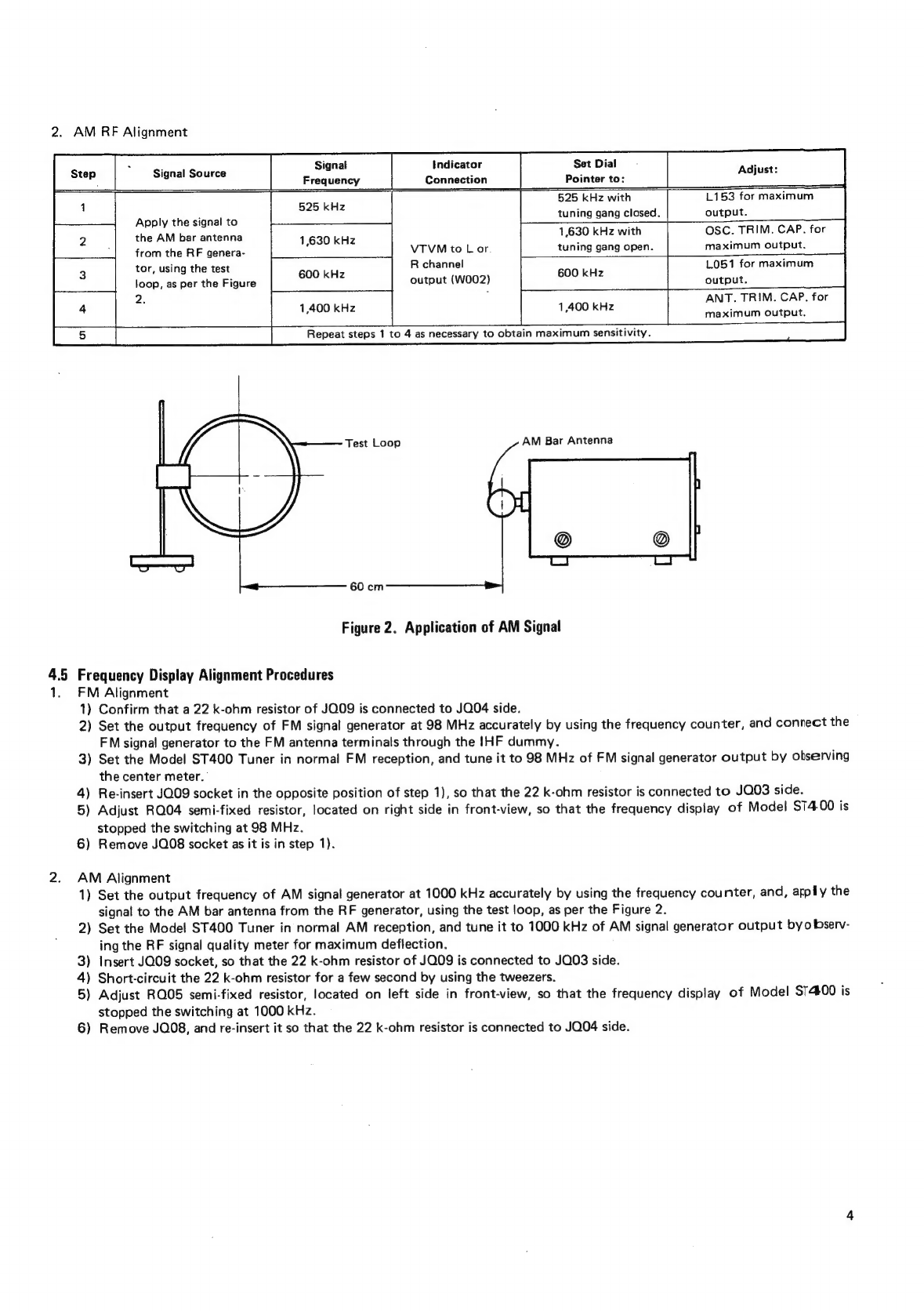
4.4
AM
Alignment
Procedures
(Selector
switch
in
the
“AM”
position)..............--
Ape
ia
Sia
iain
3
4.5
Frequency
Display
Alignment
Procedures
......
2...
ccc
ccc
eee
eee
eee
eee
eens
4
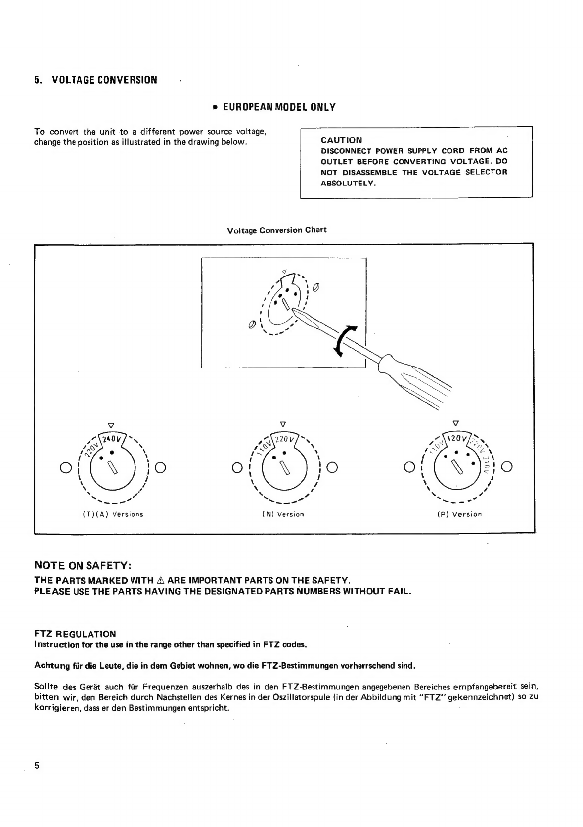
5.
VOLTAGE
CONVERSION
FOR
EUROPEAN
MODEL...........
ai
QA
le
tet
ace
Meira
ce
SaasSasest
Raia,
arkac
wrdee
5
6
SCHEMATIC
DIAGRAMS
0.0%,
cuciariss
cate
sas
oad
oa
Cees
Wane
eee
head
ha
acadedsaka
seas
6
7.
DIAGRAM
AND
COMPONENT
LOCATIONS
.............
0...
cee
cece
eee
eee
eee
eens
8
7.1.
Tuner
Assembly
(P100)
Schematic
Diagram
and
Component
Locations..............0
202
ee
neces
8
7.2
Power
Supply
Assembly
(P800)
Schematic
Diagram
and
Component
Locations..........
Mite
be
pees
9
7.3
Stereo
Survo
Led
Assembly
(PY00)
Schematic
Diagram
and
Component
Locations............-.+5+
9
7.4
Pointer
Lamp
Assembly
(PZ01)
Schematic
Diagram
and
Component
Locations.............+--+-45:
9
7.5
Switch
and
Meter
Assembly
(PS01)
Schematic
Diagram
and
Component
Locations.............-.-:
10
7.6
FM/AM
Buffer
Assembly
(PCOO)
Schematic
Diagram
and
Component
Locations.................--
10
7.7
DE-Emphasis
Assembly
(PL00)
Schematic
Diagram
and
Component
Locations.............0.-+06-
10
7.8
Frequency
Counter
Assembly
(PQ00),
Sub
Assembly
(PQ01)
Schematic
Diagram
and
Component
Locations
..........
2.0
c
cee
eee
eee
etre
eee
eee
ences
11.
B:
BLOCK
DIAGRAM:
6
ices
or
oes
ee
warn
dee
eh
We
wee
ae
Ser
ae
ewe
eadan
eta
ees
alee
ad
Seas
12
9.
EXPLODED
VIEWAND
PARTS
LIST...
1.1...
cc
eee
ee
eee
eee
ee
en
ees
13
10:
“ELEGTRIGAL
PARTS
LIST
séccc0cwe
ANA
Ass
ieee
Fe
Peale
ete
t
eae
sce
atg
te
de
tee
20
11.
TECHNICAL
SPECIFICATIONS...
5...
cee
ccc
cnc
tee
e
ence
ence
ease
eee
en
eens
25