Meanwell DBU-3200 Series User manual

DBU-3200
Instruction Manual

DBU-3200 Instruction Manual
Index
................................................................................
.................................................................................
.........................................
.......................................................................................
.......................................................................................
.......................................................................................
...............................................................
.....................................................
....................................................
.........................................................................................
........................................
...............................................................................
................................................................................
................................................................
...........................................................
...................................................................................
.........................................................................
.............................................
........................................................
......................................................
.............................................................
1
1
1
2
2
3
3
4
5
28
28
29
29
29
28
5
28
6
28
2
2
Jul. 2022 Version 3
0.Product Description
1.Notes on Operation
2.Mechanical Design and Installation Procedure
3.Derating Curve
4.Pin Assignment
5.LED Indication
6.Explanation of Operation Logic
8.PMBus and CANBus Communication Interface
9.Function Description
10.Wiring for Battery
11.Suggested Battery Capacity
12.Series and Parallel Connection
13.Troubleshotting
3.1 Charging Current vs Temperature
3.2 Charging Current vs Input Voltage
9.1 Input Voltage Range
8.1 PMbus Addressing and CAN ID setting
9.2 Power Factor Correction(PFC)
8.2 PMBus Communication Interface
9.3 Temperature Compensation
7.Charge Curve
1
0.Product Description
1.Notes on Operation
DBU-3200 is MEAN WELL's new generation intelligent battery charger with high power density.
Different battery brands and types (lead acid batteries, such as flooded, Gel, AGM, and so on, or
lithium-ion batteries, such as lithium iron, lithium manganese, and so on) may require different
charging curves and protection mechanisms for batteries, DBU-3200 is able to be accommodated
through the communication interface; parameters, such as charge voltage, charge current and taper
current, can be adjusted and the protection mechanisms for batteries can also be cancelled.
◎ The charger must be installed in a dry and well ventilated area. It should not be exposed to rain
or snow.
◎ The cables between charger and battery should be kept as short as possible to prevent excessive
voltage drop. Too much voltage drop will lead to longer charging period.
◎ Please make sure charging voltage and current meet battery specification.
◎ While charging batteries in series, do not mix old and new batteries in the same connection.
◎ When connecting or disconnecting wires, please ensure the charger is OFF.
◎ Under normal operating conditions, a 5 years warranty is offered for DBU-3200. If failure results
from improper operation, the warranty will not apply to the defective units.
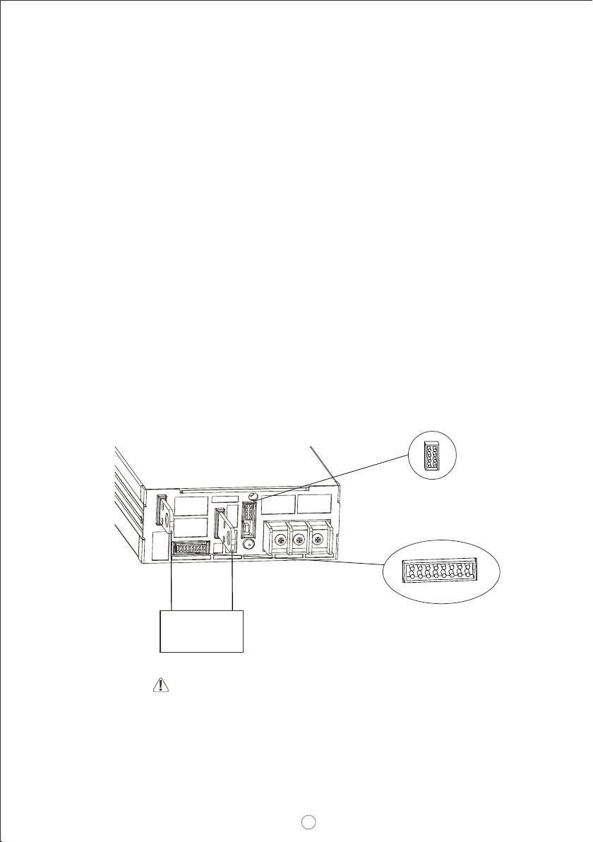
2.Mechanical Design and Installation Procedure
Warning: Before connecting a battery, please make sure
the polarity is correct to avoid damaging the charger
Figure2.1 Front panel
+
-
Batteries
CN500
CN1
8
115
2
16
2
7
1

15
16
RTH+
RTH-
Temperature sensor(NTC, 5KOhm) comes along with the charger can be connected to the unit to allow temperature
compensation of the charging voltage.
Installation Procedure:
Please make sure the charger is OFF before connecting the battery to the output terminal. Choose a
cable with suitable wire gauge according to the charging current to connect between the charger and
the battery. Battery polarity must be connected correctly:Terminal(+) to Battery(+); Terminal(-) to
Battery(-), and take notice that the positive and negative ends are not shorted.
3.Derating Curve
4.Pin Assignment
3.1 Charging current vs Temperature
3.2 Charging current vs Input Voltage
AMBIENT TEMPERATURE (℃)
LOAD (%)
LOAD (%)
INPUT VOLTAGE (VAC) 60Hz
CN1
230VAC
Input only
-30 -25 0-10 15 30 50 60 70
20
40
60
50
80
100
(HORIZONTAL) 90 100 115 180 264
80
90
100
70
60
50
40
30
1
2
15
16
2
Pin No. Function Description
4
2
7,8,9
10
5
6
3
1
12
11
Remote
ON-OFF
GND-AUX
DC-OK
T-ALARM
+5V-AUX
+12V-AUX
PV
PC
A0,A1,A2
D0
Auxiliary voltage output GND.
The signal return is isolated from the output terminals (+V & -V).
Auxiliary voltage output, 4.5~5.5V, referenced to GND-AUX (pin2).
Auxiliary voltage output, 10.6~13.2V, referenced to GND-AUX (pin2).
The maximum load current is 0.3A. This output has the built-in "Oring diodes" and is not controlled by “Remote ON-OFF
The maximum load current is 0.8A. This output has the built-in "Oring diodes" and is not controlled by “Remote ON-OFF”.
Connection for output voltage programming. (Note.1)
High (3.5 ~ 5.5V) : When the internal temperature exceeds the limit of temperature alarm, or when Fan fails.
Low (-0.5 ~ 0.5V) : When the internal temperature is normal, and when Fan works normally.
The maximum sourcing current is 10mA and only for output(Note.2)
Connection for output current programming. (Note.1)
Low (-0.5 ~ 0.5V) : When Vout ≧16V/32V ±1V. The maximum sourcing current is 10mA and only for output. (Note.2)
DC OK is associated with battery low protection.
High (3.5 ~ 5.5V) : When the Vout ≦16V/32V ±1V.
PMBus interface address lines. (Note.1)
DIP-switch interface lines for charging curve selection. (Note.1)
The unit can turn the output ON/OFF by electrical signal or dry contact between Remote ON/OFF and +5V-AUX. (Note.2)
Short (4.5 ~ 5.5V) : Power ON ; Open (-0.5 ~ 0.5V) : Power OFF ; The maximum input voltage is 5.5V.
Note1: Non-isolated signal, referenced to the [-V(signal)].
Note2: Isolated signal, referenced to GND-AUX.
13
14
+V (Signal)
-V (Signal)
Positive output voltage signal.
Negative output voltage signal.
It cannot be connected directly to the load.
It is for certain function reference; it cannot be connected directly to the load.

3
CN500 21
87
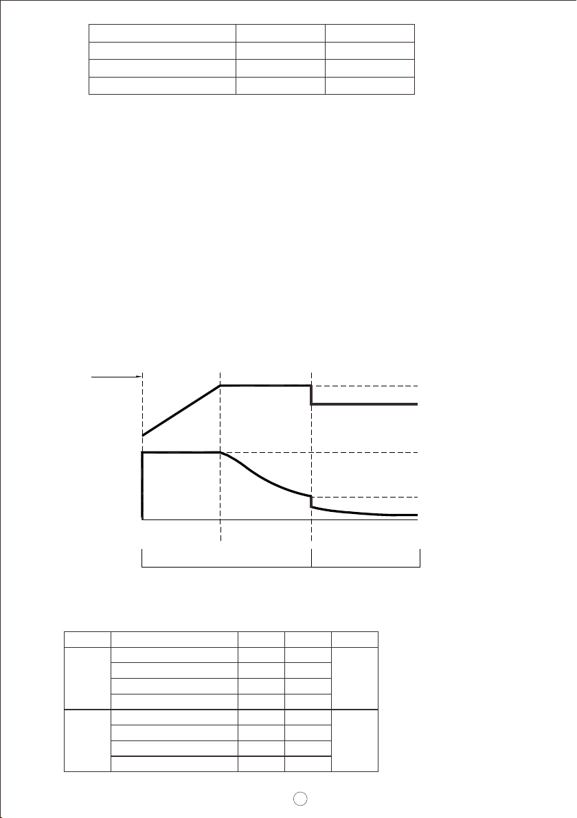
6.Explanation of Operation Logic : (3 stage charge)
5.LED Indicators
SW1
Pin No.
1,2
Function
Terminal
resistance
Description
SW1 is the selector of terminal resistor that is designed for DA/DB signals and parallel control function.
At the beginning stage of operation, the charger provides the largest current to charge the batteries,
the LED indicator will lighten in orange. After a period of time (probably a couple of hours, based on
the capacity of the batteries), charging current will decrease gradually. When the output current
reduces to 10% of its maximum value, the charger will go into “float” mode, the LED indicator will
turn to green. The relationship between charging current and charging voltage for each operation
stage is shown in the curves below:
Charge Current
Constant Current
(CURVE_CC)
stage 1 stage 2 stage 3
Constant Voltage
(CURVE_CV) (CURVE_FV)
Float
Start
Charge Voltage
100% CC
10% CC
boost
float
V
V
Orange Green
Color of LED
Pin No.
1,2
7
8
5,6
3,4
Function
DA
NC
NC
SDA
SCL
CANH
CANL
DB
-V (Signal)
Description
Differential digital signal for parallel control.
Differential digital signal for parallel control.
For standard model: None.
For standard model: None.
For PMBus model: Serial Data used in the PMBus interface. (Note)
For PMBus model: Serial Clock used in the PMBus interface. (Note)
For CANBus model: Data line used in CANBus interface. (Note)
For CANBus model: Data line used in CANBus interface. (Note)
Negative output voltage signal.
It is for local sense; and certain function reference; it cannot be connected directly to the load.
LED
Green
Orange
Red
Float (stage 3)
Charging (stage 1 or stage 2)
Description
Abnormal status (OTP, OLP, Fan Fail, Charging timeout)
Note: Isolated signal, referenced to GND-AUX.
◎ Embedded 3 stage charging curve
4
7.Charge Cureve
The factory setting is “default”, which can be programmed via PMBus.
◎ Default 3 stage charging curve
Charge Current
Start
Charge Voltage
Color of LED
Constant Current
(CURVE_CC)
stage 1 stage 2 stage 3
Constant Voltage
(CURVE_CV) (CURVE_FV)
Float
100% CC
10% CC
boost
float
V
V
Orange Green
Explanation for 3 stage charge curve
(0) Initial stage (battery analysis):Check battery voltage level to see whether there is a battery
connected.
(1) Stage 1 (constant current):A constant current is provided so that the battery can be quickly
charged to 2.4V per cell.
(2) Stage 2 (constant voltage):A constant voltage of 2.4V per cell is provided until the charging
current gradually reduces to 10%.
(3) Stage 3 (float):The output voltage switches to the float voltage, making it 2.3V per cell to keep the
battery fully charged.
Note: By factory default, PIN10 and PIN14 on CN1 are connected.
MODEL
24V
48V
Vboost
28.8
57.6
28
56
28.4
56.8
29
58
Vfloat
27.6
55.2
27.2
54.4
26.8
53.6
27
54
Description
Default, programmable
Default, programmable
#1 Pre-defined, gel batter
#1 Pre-defined, gel batter
#2 Pre-defined, flooded battery
#2 Pre-defined, flooded battery
#3 Pre-defined, AGM battery
#3 Pre-defined, AGM battery
CC(default)
110A
55A
STATUS
BOOST CHARGE VOLTAGE
FLOAT CHARGE VOLTAGE
28.8V
27.6V
DBU-3200-24
57.6V
55.2V
DBU-3200-48
Figure Charge Curve 6.1
CONSTANT CURRENT 110A 55A

5
8.Communication Protocol
8.1 PMbus Addressing and CAN ID setting
◎Each DBU-3200 unit should have their unique and own device address or ID to communicate over the bus.
*PMbus 7-bit addressing definition :
*CAN message ID definition :
1
MSB
0 0 0 A2 A1 A0
LSB
Users can use three different methods to control outputs of DBU-3200. The control priority between
the methods is as follows: Communication (PMBus or CAN bus) > PV/PC > SVR. These three control
methods can be used interchangeably. When using communication control, it is essential to
communicate with the device within 4 seconds. Otherwise, the program will reset the control priority
and set the communication parameters back to the factory default values(NOTE 1). However, the
following condition will bypass this control logic: setting DBU-3200 to charger mode. In charger
mode, PV/PC and SVR controls will become inactive and charging-related settings can only be
changed via communication.
NOTE: 1.When D0 is set at “1” and communication function is used, some of the parameters will
return to the factory default values if any of the conditions happens, AC recycling and
communication timeout. Take DBU-3200-24 as an example, command OPERATION
becomes ON, Vo and Io change to 24V and 110A.
2.In charger mode, Remote ON/OFF or OPERATION ON/OFF can be used to activate new
curve procedures and import parameters and settings for a new curve profile. Additionally,
it can also release protections caused by CURVE_CC_TIMEOUT, CURVE_CV_TIMEOUT,
or CURVE_TP_TIMEOUT due to timeouts.
Message ID
0xC00XX
0xC01XX
0xC01FF
Description
DBU-3200 to Controller Message ID
Controller to DBU-3200 Message ID
Controller broadcasts to DBU-3200
XX means the CAN ID of DBU-3200
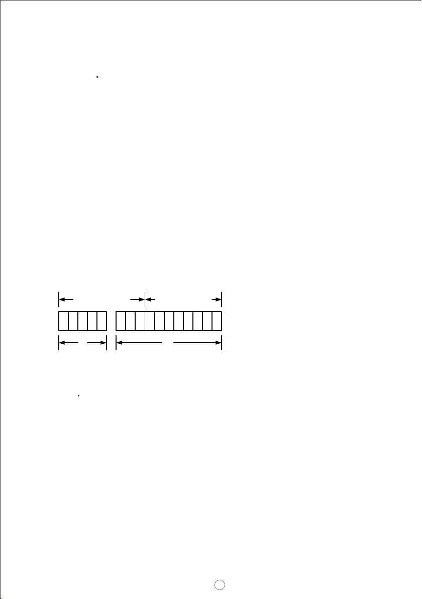
A0-A2 allows users to designate an address or ID for the DBU-3200 unit; these three bits are
defined through PIN7 (A0), PIN8 (A1) and PIN9 (A2) on CN1. There are up to 8 different
addresses are available to be assigned. When connecting one of these pins, for example, PIN8
with PIN14 (-V(Signal)), the corresponding bit, A1, is set to logic “0”; when it is kept opened, for
example, PIN7, the corresponding bit, A0, is set to logic “1”. Please refer to Table 8-1(left) for
detailed setup.
◎Charge mode can be activated by settings over D0 (PIN10) on CN1. When D0 is logic “0”,
connecting PIN10 to PIN14(-V(Signal)), DBU-3200 follows a built-in charging curve to
charge the batteries; when D0 is logic “1”, PIN10 kept opened, operation of the unit is
completely defined by the control over PMBus, PV/PC or SVR. Please refer to Table 8-
1(right).

Module
No. A0
0
1
2
3
4
5
6
7
A1 A2
0
0
0
0
1
1
1
1
0
0
0
0
1
1
1
1
0
0
0
0
1
1
1
1
Device address/ID
Table 8-1
D0 Function describe
0 Charging curve
1 PMBus or PV/PC or SVR control
Charging Curve
When it is opted for charging curve, D0 set to 0, charging curve function is enabled with additional
PMBus or CAN bus commands. There are 4 built-in charging curves, “default” curve, one pre-
defined curve for “gel battery”, one pre-defined curve for “flooded battery” and one pre-defined
curve for “AGM battery”. Each curve can be selected by Command CURVE_CONFIG (PM: B4h;
CAN: 0x00B4). In addition, users are able to customize their own charge curves, which will be
stored to “default” after modification. Constant voltage level can be set by Command CURVE_CV
(PM:B1h; CAN: 0x00B1); Float voltage level can be set by Command CURVE_FV (PM:B2h; CAN:
0x00B2) ;Charge current level of stage1 can be set by Command CURVE_CC(PM:B0h; CAN:
0x00B0);Taper current level from stage2 to stage3 can be set by Command CURVE_TC(PM:B3h;
CAN: 0x00B3)). Please refer to the command list of PMBus or CAN bus for detailed information on
commands and parameters.
NOTE:
1. The updated charging parameters is saved into EEPROM. The updated charging curve takes
effect after DBU-3200 is restarted, remoted on/off or operation on/off.
2. When charging curve is enabled, the following commands will be invalid while other commands
are still effective: Command VOUT_TRIM(22h)/ (regarding Output VOUT_SET(0x0020)
voltage programming function) and Command IOUT_OC_FAULT_LIMIT(46h)/
IOUT_SET(0x0030) (regarding Output current programming function).
8.2 PMBus Communication Interface
◎DBU-3200 is compliant with PMBus Rev.1.1, the maximum communication speed is 100KHz and
the maximum number of assignable addresses is up to 8 units on a bus.
◎PMBus communication interface is able to provide the current operating status and information as
follows:
1. Output voltage, current and internal temperature.
2.Alarm and status.
3.Manufacturer's and model data.
4. Read/write of charge curve settings.
6

7
47h
79h
7Ah
7Bh
7Ch
7Dh
1
2
1
1
1
1
Define protection and response when an
output overcurrent fault occurred
Summary status reporting
Output voltage status reporting
Output current status reporting
AC inpit voltage statusreporting
Temperature status reporting
IOUT_OC_FAULT_RESPONSE
STATUS_WORD
STATUS_VOUT
STATUS_IOUT
STATUS_INPUT
STATUS_TEMPERATURE
R Byte
R Word
R Byte
R Byte
R Byte
R Byte
22h 2 Output voltage trimmed value
(format: Linear 16, N= -9)
VOUT_TRIM R/W Word
46h 2Output overcurrent setting value
(format: Linear 11, N= -2)
IOUT_OC_FAULT_LIMIT R/W Word
7Eh 1 Communication, logic,
Memory status reporting
STATUS_CML R Byte
Command
Code
01h
02h
19h
20h
21h
# of data
Bytes
1
1
1
1
2
Description
Remote ON/OFF control
ON/OFF function configuration
Capabilities of a PMBus device
Define data format for output voltage
(format: Linear 16, N= -9)
Output voltage setting value
(format: Linear 16, N= -9)
Command
Name
OPERATION
ON_OFF_CONFIG
CAPABILITY
VOUT_MODE
VOUT_COMMAND
Transaction
Type
R/W Byte
Read Byte
Read Byte
R Byte
R Word
Table 8-2
◎PMBus commands: The command list of the DBU-3200 is shown in Table 8-2. It is compliant
with the standard protocol of PMBus Rev. 1.1. For more detailed information, please refer to
PMBus official website (http://pmbus.org/specs.html)
90h
91h
98h
2
2
1
Fan speed 1 reading value
(format: Linear 11, N= 5)
Fan speed 2 reading value
(format: Linear 11, N= 5)
The compliant revision of the PMBus
(default: 11h for Rev. 1.1)
READ_FAN_SPEED_1
READ_FAN_SPEED_2
PMBUS_REVISION
R Word
R Word
R Byte
99h
9Ah
9Bh
9Ch
9Dh
9Eh
12
12
6
3
6
12
Manufacturer's name
Manufacturer's model name
Firmware revision
Manufacturer's factory location
Manufacture date. (format: YYMMDD)
Product serial number
MFR_ID
MFR_MODEL
MFR_REVISION
MFR_LOCATION
MFR_DATE
MFR_SERIAL
Block Read
Block Read
Block Read
Block R/W
Block R/W
Block R/W
81h
80h
88h
8Bh
8Ch
1
1
2
2
2
Fan1 and 2 status reporting
Manufacture specific status reporting
AC input voltage reading value
(format: Linear 11, N=-1)
Output voltage reading value
(format: Linear 16, N= -9)
Output current reading value
(format: Linear 11, N= -2)
STATUS_FANS_1_2
STATUS_MFR_SPECIFIC
READ_VIN
READ_VOUT
READ_IOUT
R Byte
R Byte
R Word
R Word
R Word

◎ Definition of Command B4h CURVE_CONFIG:
Note:
Bit7 Bit6 Bit5 Bit4 Bit3 Bit2 Bit1 Bit0
High byte - - - - - FVTOE CVTOE CCTOE
Low byte - STGS - - TCS CUVS
Low byte
Bit 1-0 CUVS :Charge Curve selecting
00=Customized Charge Curve (default)
01=Gel Battery
10=Flooded Battery
11=AGM Battery
Bit 3-2 TCS:Temperature Compensation setting
Bit 6 STGS:2/3 stage charge setting
High byte
00= disable
0= 3 (default, Curve_VBST and CURVE_V FLOAT) stage charge
Bit 0 CCTOE:Constant Current Stage timeout indication enable
Bit 1 CVTOE:Constant Voltage Stage timeout indication enable
Bit 2 FTTOE:Float Stage timeout indication enable
01= -3 mV/℃/cell (default)
1= 2 (only CURVE_VBST) stage charge
0= (default)disabled
0= (default)disabled
0= (default)disabled
1= enabled
1= enabled
1= enabled
10= -4 mV/℃/cell
11= -5 mV/℃/cell
Command
Code
# of data
Bytes Description
Command
Name
Transaction
Type
B8h 2Charger's status reportingCHG_STATUS READ Word
B4h
B5h
B6h
B7h
B3h
2
2
2
2
Configuration setting of charging curve
CC stage timeout setting value of charging curve
(format: Linear, N= 0)
CV stage timeout setting value of charging curve
(format: Linear, N= 0)
Floating timeout setting value of charging curve
(format: Linear, N= 0)
CURVE_CONFIG
CURVE_CC_TIMEOUT
CURVE_CV_TIMEOUT
CURVE_FLOAT_TIMEOUT
R/W Word
R/W Word
R/W Word
R/W Word
B0h
B1h
B2h
Valid when charging according to charge curve (D0=0)
2
Taper current setting value of charging curve
(format: Linear, N= -2)
CURVE_TC R/W Word
2
2
2
Constant current setting value of charging curve
(format: Linear, N= -2)
Constant voltage setting value of charging curve
(format: Linear, N= -9)
Constant voltage setting value of charging curve
(format: Linear, N= -9)
CURVE_CC
CURVE_CV
CURVE_FV
R/W Word
R/W Word
R/W Word
8

Bit 2 CVM:Constant Voltage Mode Status
0=the charger NOT in constant voltage mode
1=the charger in constant voltage mode
Bit 3 FVM:Float Mode Status
0=the charger NOT in float mode
1=the charger in float mode
High byte
Bit 0 EEPER: EEPROM Charge Parameter Error
Bit 2 NTCER: Temperature Compensation Status
Bit 3 BTNC: Battery Detection
Bit 5 CCTOF:Time-out Flag of Constant Current Mode
Bit 6 CVTOF:Time-out Flag of Constant Voltage Mode
Bit 7 FTTOF:Time-out Flag of Float Mode
0=data of charge parameter correct
0=NO short-circuit in the circuitry of temperature compensation
0=battery detected
0=time-outNO in constant current mode
0=time-outNO in constant voltage mode
0= NO time-out in float mode
1=data of charge parameter error
1=the circuitry of temperature compensation has short-circuited
1=NO battery detected
1=constant current mode timed out
1=constant voltage mode timed out
1=float mode timed out
Bit7 Bit6 Bit5 Bit4 Bit3 Bit2
High byte FVTOF CVTOF CCTOF - NTCERBTNC
CVMFVM
Low byte - - - -
Low byte
Bit 0 FULLM:Fully Charged
0=NOT fully charged
1=fully charged
Bit 1 CCM:Constant Current Mode Status
0=the charger NOT in constant current mode
1=the charger in constant current mode
◎ Definition of Command B8h CHG_STATUS:
Bit1 Bit0
-
CCM
EEPER
FULLM
9

Note:
EEPER:When EEPROM Charge Parameter Error occurs, the charger stops charging the battery and
the LED indicator turns red. The charger needs to re-power on to re-start charging the
battery.
NTCER:When Temperature Compensation Short occurs, the charger output will shut down and the
LED indicator will turn red. The charger will automatically restart after the Temperature
Compensation Short condition is removed.
BTNC:When there is no battery detected, the charger stops charging the battery and the LED
indicator turns red. The charger needs to re-power on to re-start charging the battery.
CCTOF:When timeout arises in the Constant Current stage, the charger stops charging the battery
and the LED indicator turns red. The charger needs to re-power on to re-start charging the
battery.
CVTOF:When timeout arises in the Constant Voltage stage, the charger stops charging the battery
and the LED indicator turns red. The charger needs to re-power on to re-start charging the
battery.
FVTOF:When timeout arises in the Float stage, the charger stops charging the battery and the LED
indicator turns green. This charging flow is finished; the charger needs to re-power on to
start charging a different battery.
10

PMBus command
OPERATION
CURVE_CV
(Note. 3)
CURVE_FV
(Note. 3)
IOUT_OC_FAULT_LIMIT
CURVE_CC
CURVE_TC
CURVE_CC_TIMEOUT
CURVE_CV_TIMEOUT
CURVE_FLOAT_TIMEOUT
VOUT_COMMAND
(Note. 2)
VOUT_TRIM
(Note. 2)
Adjustable range
00h(OFF) / 80h(ON)
9 ~ 15V
9 ~ VBST
20 ~ 100A
5 ~ 30A
18 ~ 30V
18 ~ VBST
11 ~ 55A
2.75 ~ 16.5A
60 ~ 64800 Minute
36 ~ 60V
36 ~ VBST
5.5 ~ 27.5A
1.5 ~ 8.3A
-3 ~ 3V
-6 ~ 6V
-12 ~ 12V
Tolerance Default
N/A
N/A
N/A
N/A
80h(ON)
±0.18V
±0.18V
±2.5A
±2.5A
±0.36V
±0.36V
±1.34A
±1.34A
±5 Minute
±0.48V
±0.48V
±0.67A
±0.67A
14.4V
13.8V
100A
10A
28.8V
27.6V
55A
5.5A
600 Minute
57.6V
55.2V
27.5A
2.8A
±0.18V
±0.36V
±0.48V
0V
0V
0V
Model
ALL
12V 12V 12V
12V
12V
12V
12V
12V
24V 24V 24V
24V
24V
24V
24V
24V
ALL
48V 48V 48V
48V
48V
48V
48V
48V
◎ Control parameter
Table 8-4
READ_FAN_SPEED_1
READ_FAN_SPEED_2
READ_VOUT
READ_IOUT
(Note. 1)
0 ~ 26500RPM
0 ~ 26500RPM
0 ~ 150A
0 ~ 30V
0 ~ 80A
0 ~ 60V
0 ~ 40A
±2000RPM
±2000RPM
±2.5A
±0.36V
±1.34A
±0.48V
±0.67A
ALL
ALL
12V
24V
24V
48V
48V
PMBus Data Range and Tolerance
◎ Display parameters
PMBus command
READ_VIN
Range
80 ~ 264V
0 ~ 15V
Tolerance
±10V
±0.18V
Model
ALL
12V
Table 8-3
11

Minimum readable currentModel
24V 2.7A±1A
48V 1.3A±1A
1.READ_IOUT will display ZERO amp when output current is less than values in the table below:
Note:
Adjustable voltage rangeModel
24V 18 ~ 30V
48V 36 ~ 60V
2.
When using PMBus to adjust output voltage, VOUT_COMMAND only can be used to display the
rated voltage of the unit and cannot be . It is VOUT_TRIM that swritten ets up the amount of
trimmed voltage. Taking DBU-3200-24 as an example, to get a 18V output, please set value of
VOUT_TRIM to -6V Adjustable voltage range for each model is shown as below:.
3.The value of CURVE_FV should be set less or equal to CURVE_CV,If CURVE_FV is greater
than CURVE_CV, it will be saved as CURVE_FV = CURVE_CV in EEPROM.
Notes on PMBus
1.Insert a at least 50msec delay between commands
2. Examples for Format Conversion :
(1) LINEAR16 format:VOUT_COMMAND、VOUT_TRIM、READ_VOUT、CURVE_CV、CURVE_FV.
N
Actual voltage = communication reading V × 2 . There are two definitions in the VOUT_MODE
command that refer to N requirements.
VOUT_MODE
Data Byte For
Linear Mode
0 0 01 1 12 2 23 3 34 4 45 5 56 6 67 7 7
Mode
=000b
VOUT_COMMAND Data Bvtes
For Linear Mode
MantissaExponent
VN
Data Byte High Data Byte Low
12
Linear Format Data Bytes
The Mode bits are set to 000b.
The Voltage, in volts, is calculated from the equation:
N
2
Voltage V=
Where:
Voltage is the parameter of interest in volts;
V is a 16 bit unsigned binary integer; and
N is a 5 bit two's complement binary integer.
N
EX: Vo_real (actual output voltage) = V x 2 , V is from READ_VOUT. N If VOUT_MODE = 0x17,
-9
meaning N is -9. READ_VOUT is 0x3000 12288, then Vo_real =12288 × 2 =24.0V.
(2)LINEAR11 format:IOUT_OC_FAULT_LIMIT、READ_VIN、READ_IIN、READ_IOUT、
READ_TEMPERATURE_1、READ_FAN_SPEED_1、READ_FAN_SPEED_2、CURVE_CC
、CURVE_TC、CURVE_CC_TIMEOUT 、CURVE_CV_TIMEOUT 、
CURVE_FV_TIMEOUT。
N
Actual value X = communication read value Y x 2 . Among them, the definition of the description
column for each aircraft type is referred to
N
EX: Io_real (actual output current) = Y× 2 , Y is from READ_IOUT. N If READ_IOUT is 0xF188h, meaning N is -2 and
-2
Y is 0x0188. Y is 0x0188 → 392, then Io_real = 392 × 2 = 98.0A.
76543 21076543210
N Y
Data Byte High Data Byte Low
MSB
MSB
Linear Data Format Data Bytes Y, N and the "real world" value is:
The relation between
X = Y 2 N
Where, as described above:
X is the "real world" value;
Y is an 11 bit, two's complement integer; and
N is a 5 bit, two's complement integer.
Devices that use the Linear format must accept and be able to process any value of N.
13

Communication Example - Practical Operation of Charger Mode
The following steps will describe how to set the DBU-3200-48 to charger mode and adjust its curve for a
2-stage charging process, with a constant current (CC) of 30A and a constant voltage (CV) of 56V.
1.Set the address of the charger to “0” and set it to charge mode.
2.Connect the SDA, SCL and GND pins of the master to the corresponding SDA (PIN7) and SCL
(PIN8) of CN500 and GND-AUX (PIN2) of CN1 on the charger.
◎Set speed: 100KHz
DBU-3200
SDA(CN500)
7
8
2
SDA
SCL(CN500)SCL
GND-AUX(CN1)GND
Controllor
3.Communication function can be accessed immediately after is connected to AC. Frist set DBU-3200
the charger to 2-stage charging mode.
4.Set the constant current (CC) point to 30A.
Command code: 0xB4(CURVE_CONFIG)
Data: 44(Lo) + 00(Hi). Please refer to definition of CURVE_CONFIG for detailed information.
Command code: 0xB0(CHURVE_ICHG)
Data: 30A → 0x78(Lo) + 0xF0(Hi)
NOTE: CURVE_ICHG is LINEAR11 format
Address(7 bit)
Address(7 bit)
0x40
0x40
Operation
Operation
Write
Write
Command Code
Command Code
0xB4
0xB0
Data
Data
0x44, 0x00
0x78, 0xF0
DBU-3200
A0(CN1)
A1(CN1)
A2(CN1)
D0(CN1)
-V-signal(CN1)
7
8
9
10
14
14

6.Before connecting to the batteries, it is recommended to review all of the settings and parameters
using the appropriate commands. In the event that they do not meet your requirements, you may
rewrite them as needed. EX: Read CHURVE_VBST to check whether CV level or Vboost was set to a
proper level.
7.Finally, short circuit Remote ON-OFF (PIN4) and +5-AUX (PIN3) pins of the CN1 connector on the
charger to remote on it to charge the batteries.
Read CURVE_VBST
The unit returns data below
-9
Data: 0x00(Lo) + 0x70(Hi) → 0x7000 → 28672 × 2 = 56V。
5. Set the constant voltage (CV) point to 56V.
Command code: 0xB1(CHURVE_VBST)
Data: 56V → 0x00(Lo) + 0x70(Hi)
NOTE: CHURVE_VBST is LINEAR16 forma
Address(7 bit)
Address(7 bit)
Address(7 bit)
0x40
0x40
0x40
Operation
Operation
Write
Read
Command Code
Command Code
0xB1
0xB1
Data
Data
0x00, 0x70
0x00, 0x70
Remote ON-OFF
CN1 +5V-AUX
DBU-3200
3
4
15

This protocol follows CAN ISO-11898 with Baud rate of 250Kbps.
◎Data Frame
◎Communication Timing
This protocol uses Extended CAN 29-bit identifier frame format or CAN 2.0B.
Min. request period (Controller to DBU-3200): 50mSec。
Max. response time (DBU-3200 to Controller): 12.5mSec。
Min. packet margin time (Controller to DBU-3200): 12.5mSec。
PSU CAN-RX
(form Controller)
PSU CAN-TX
Request period
(Controller to PSU/CHG)
Response time
(PSU/CHG to Controller)
RX data
TX data
RX data
Packet Margin time
(Controller to PSU/CHG)
8.3 CANBus Communication Interface
◎Physical layer specification
◎Data Field Format
Controller to DBU-3200
Write :
COMD. low byte
COMD. low byte
COMD. high byte
COMD. high byte
Data low byte Data high byte
Data filed bytes
Data filed bytes
Read:
0
0
1
1
2 3
16

8.3.1 CANBus Command list
Command
Code
0x0000
0x0020
0x0030
0x0050
0x0060
0x0061
0x0062
0x0070
0x0071
0x0080
0x0081
0x0082
0x0083
0x0040
# of data
Bytes
1
2
2
2
2
2
2
2
2
6
6
6
6
2
Description
ON/OFF control
ON: 01h
OFF: 00h
Output voltage set
(format: value, F=0.1)
Output current set
(format: value, F=0.1)
Input voltage read value
(format: value, F=1)
Output voltage read value
(format: value, F=0.1)
Output current read value
(format: value, F=0.1)
Internal ambient temperature
(format: value, F=0.1)
Fan speed 1 reading value
(Format: value, F=1, unit: RPM)
Fan speed 2 reading value
(Format: value, F=1, unit: RPM)
Manufacture's name
Manufacture's name
Manufacture model name
Manufacture model name
Abnormal status
Command
Name
OPERATION
VOUT_SET
IOUT_SET
READ_VIN
READ_VOUT
READ_IOUT
READ_
TEMPERATURE_1
READ_FAN_SPEED_1
READ_FAN_SPEED_2
MFR_ID_B0B5
MFR_ID_B6B11
MFR_MODEL_B0B5
MFR_MODEL_B6B11
FAULT_STATUS
Transaction
Type
R/W
R/W
R/W
R
R
R
R
R
R
R
R
R
R
R
0x0085
0x0086
3
6
Manufacture place
Manufacture date
MFR_LOCATION_B0B2
MFR_DATE_B0B5
R
R
0x0084 6Firmware version
MFR_REVISION_B0B5 R
COMD. low byte COMD. high byte Data low 1 ..... Data high 6
Data filed bytes
Response:
DBU- 0032 to Controller
NOTE: DBU-3200 will not send data back when writing parameters, such as VOUT_SET
0 1 2 7
17

0x00B5
0x00B6
0x00B7
0x00B8
2
2
2
2
CC charge timeout setting of charging curve
(format: value, F=1)
(format: value, F=1)
(format: value, F=1)
CV charge timeout setting of charging curve
FV charge timeout setting of charging curve
Charging status reporting
CURVE_CC_TIMEOUT
CURVE_CV_TIMEOUT
CURVE_FV_TIMEOUT
CHG_STATUS
R/W
R/W
R/W
R
Table 8-8
Command
Code
# of data
Bytes Description
Command
Name
Transaction
Type
0x00B0
0x00B1
0x00B2
0x00B3
0x00B4
2
2
2
2
2
Constant current setting of charge curve
(format: value, F=0.1)
Constant voltage setting of charge curve
(format: value, F=0.1)
Floating voltage setting of charge curve
(format: value, F=0.1)
Taper current setting of charge curve
(format: value, F=0.1)
Configuration setting of charge curve
CURVE_CC
CURVE_CV
CURVE_FV
CURVE_TC
CURVE_CONFIG
R/W
R/W
R/W
R/W
R/W
Valid when charging according to charge curve(D0=ON)
Bit 0 FAN_FAIL:Fan locked flag
0 =Working normally
1=Fan locked
Bit 1 OTP:Over temperature protection
0 =Internal temperature normal
1=Internal temperature abnormal
Bit 2 OVP:DC over voltage protection
0=DC voltage normal
1=DC over voltage protected
Bit 3 OLP:DC over current protection
0 =DC current normal
1=DC over current protected
Bit7 Bit6 Bit5 Bit4 Bit3 Bit2
Low byte OVPOLPSHORTAC_FAILOP_OFFHI_TEMP
◎Definition of Command FAULT_STATUS(0x0040):
8.3.2 Definition and contents of CANBus Command list
Bit1
OTP
FAN_FAIL
Bit0
0x0088 6Manufacture serial number
MFR_SERIAL_B6B11 R
0x0087 6Manufacture serial number
MFR_SERIAL_B0B5 R
18
Other manuals for DBU-3200 Series
1
Table of contents
Other Meanwell Batteries Charger manuals

Meanwell
Meanwell NPB-450 NFC Series User manual

Meanwell
Meanwell RPB-1600 Series User manual

Meanwell
Meanwell PB-1000 User manual

Meanwell
Meanwell PB-230 User manual

Meanwell
Meanwell PB-1000-12 User manual

Meanwell
Meanwell NPB Series User manual

Meanwell
Meanwell ENC Series User manual

Meanwell
Meanwell GC160 User manual

Meanwell
Meanwell PA-120 User manual

Meanwell
Meanwell DBU-3200 Series User manual


