Microchip Technology TC7660S Series User manual
Other Microchip Technology Control Unit manuals
Microchip Technology
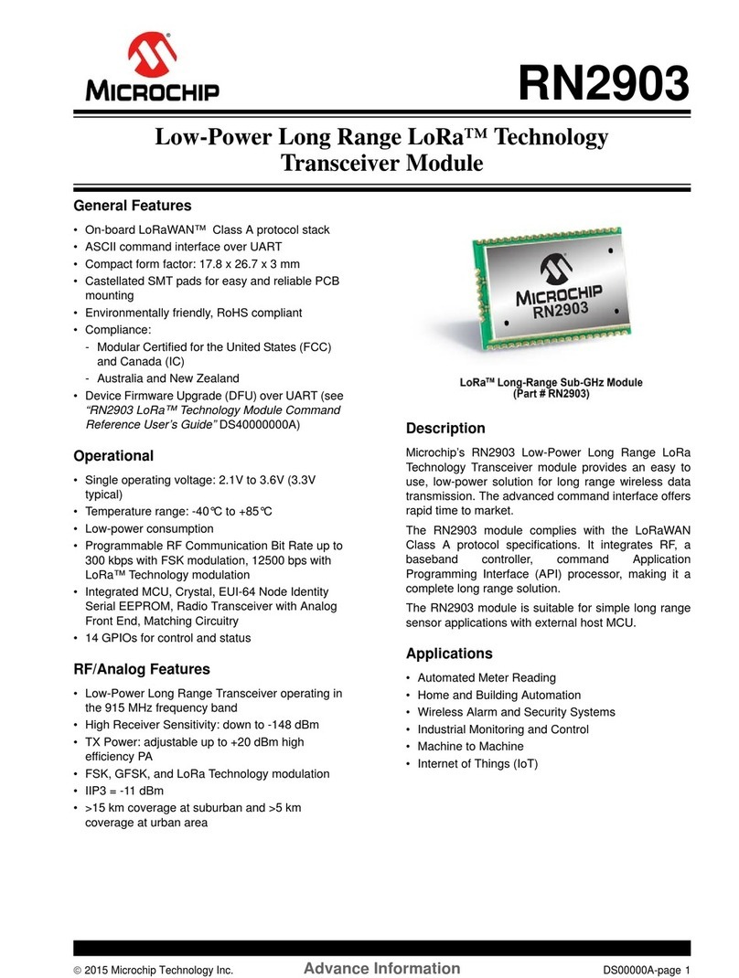
Microchip Technology RN2903 User manual
Microchip Technology
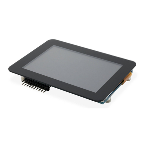
Microchip Technology maXTouch Curiosity Pro User manual
Microchip Technology
Microchip Technology LoRa User manual
Microchip Technology
Microchip Technology dsPICDEM MC1H User manual
Microchip Technology
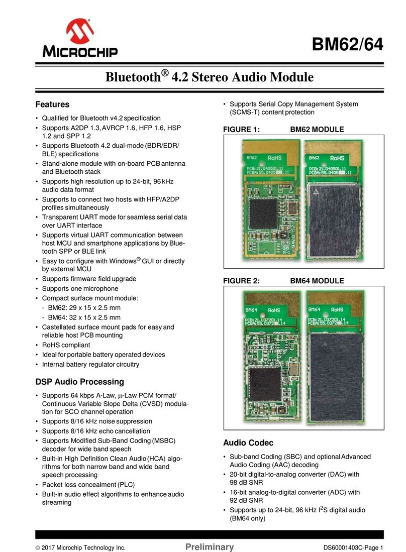
Microchip Technology BM62 User manual
Microchip Technology
Microchip Technology MCP19035 User manual
Microchip Technology
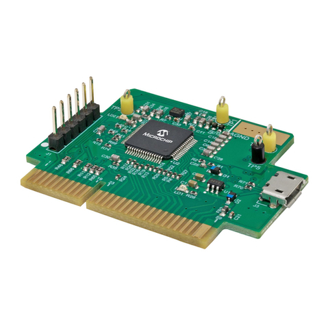
Microchip Technology RN4870 User manual
Microchip Technology
Microchip Technology dsPIC33EP128GS806 User manual
Microchip Technology
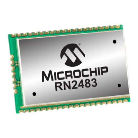
Microchip Technology RN2483 LoRa User manual
Microchip Technology
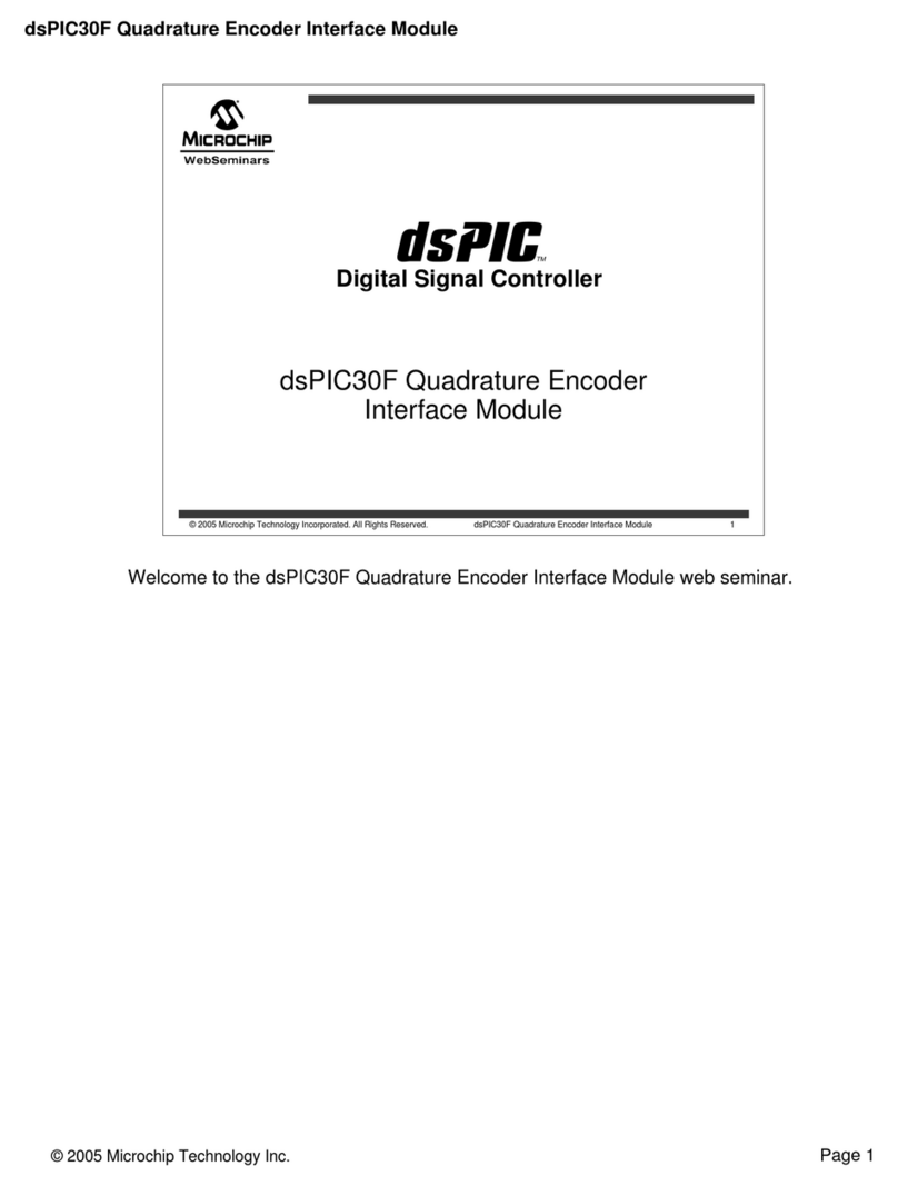
Microchip Technology dsPIC30F User manual
Microchip Technology
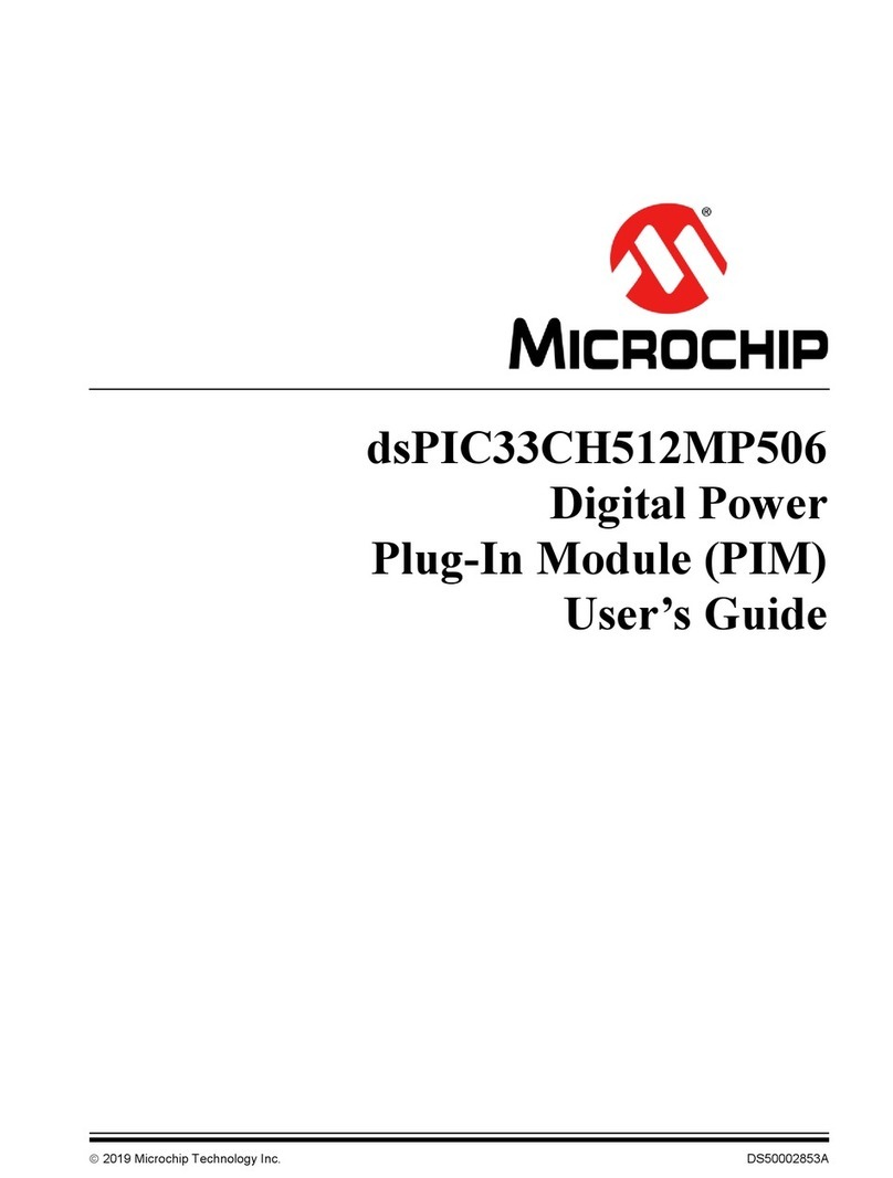
Microchip Technology dsPIC33CH512MP506 User manual
Microchip Technology
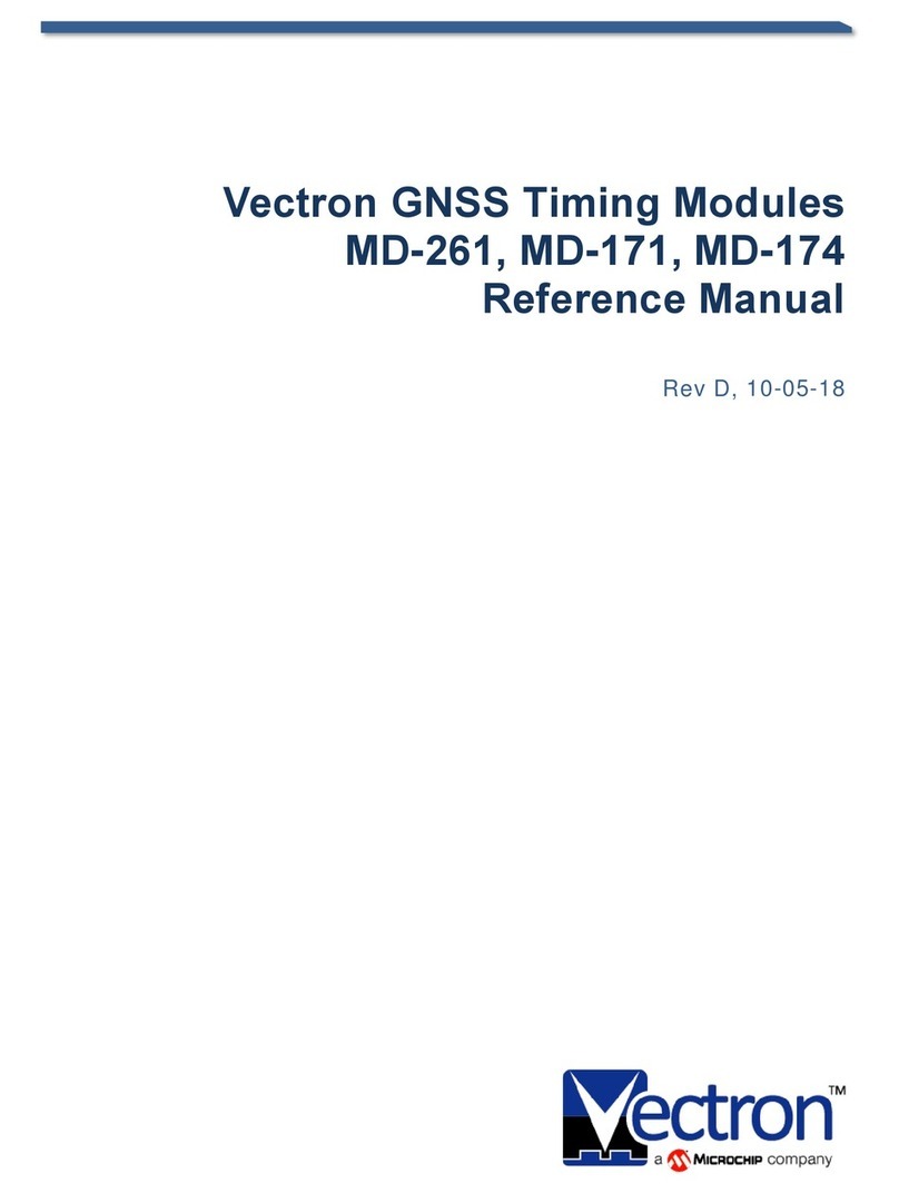
Microchip Technology Vectron MD-261 User manual
Microchip Technology
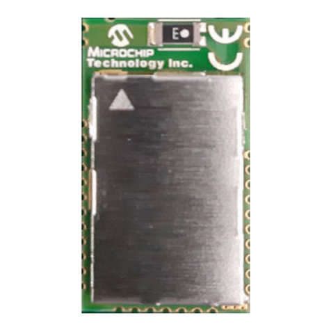
Microchip Technology BM78SPP05MC2-0001AA User manual
Microchip Technology
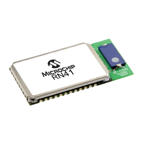
Microchip Technology RN41 User manual
Microchip Technology
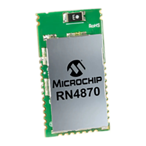
Microchip Technology RN4870/71 User manual

Microchip Technology
Microchip Technology MRF24XA PICtail User manual
Microchip Technology
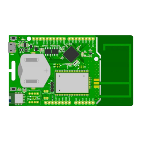
Microchip Technology ExpLoRer User manual
Microchip Technology
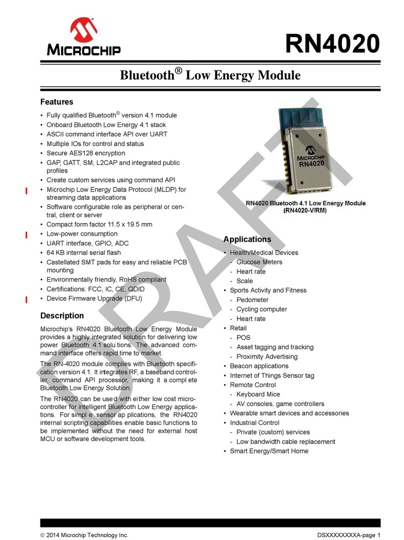
Microchip Technology RN4020 User manual
Microchip Technology
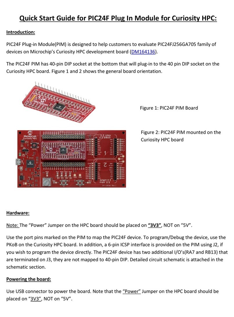
Microchip Technology PIC24F User manual
Microchip Technology
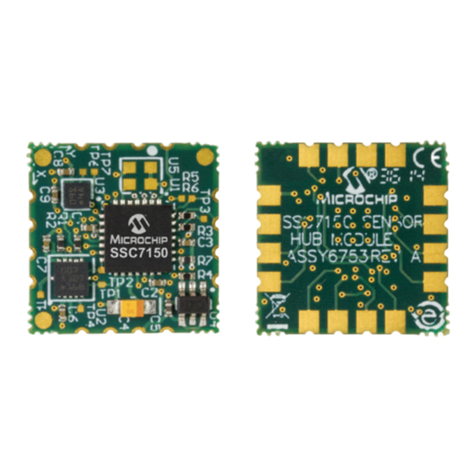
Microchip Technology MM7150 User manual
Popular Control Unit manuals by other brands
Festo
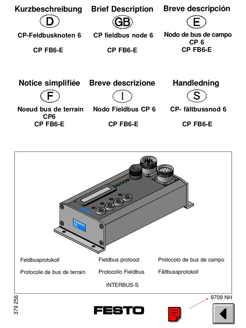
Festo Compact Performance CP-FB6-E Brief description
Elo TouchSystems
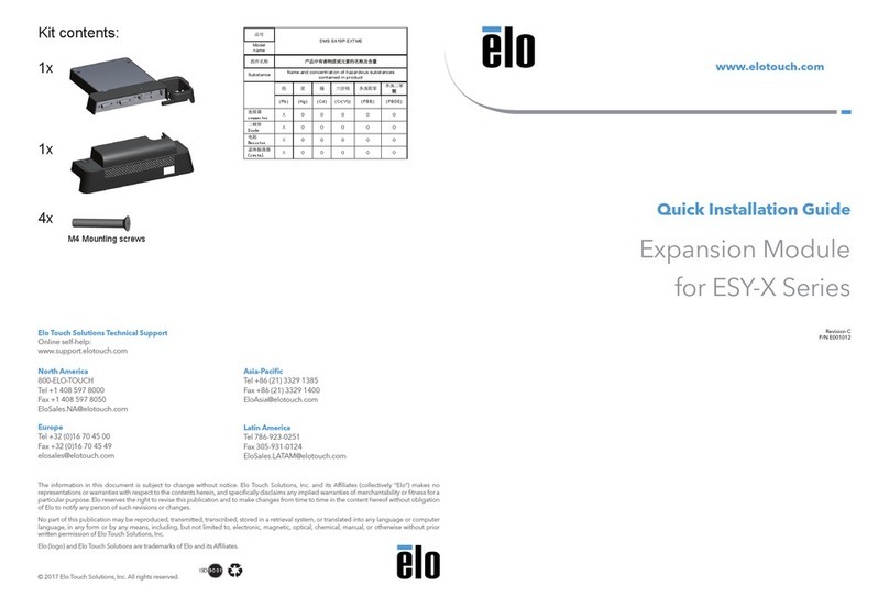
Elo TouchSystems DMS-SA19P-EXTME Quick installation guide
JS Automation
JS Automation MPC3034A user manual
JAUDT
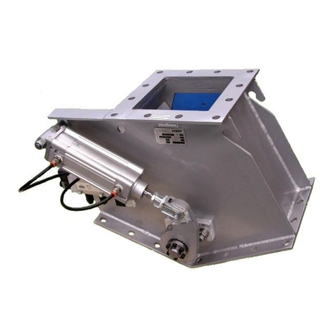
JAUDT SW GII 6406 Series Translation of the original operating instructions
Spektrum
Spektrum Air Module System manual
BOC Edwards
BOC Edwards Q Series instruction manual

KHADAS
KHADAS BT Magic quick start
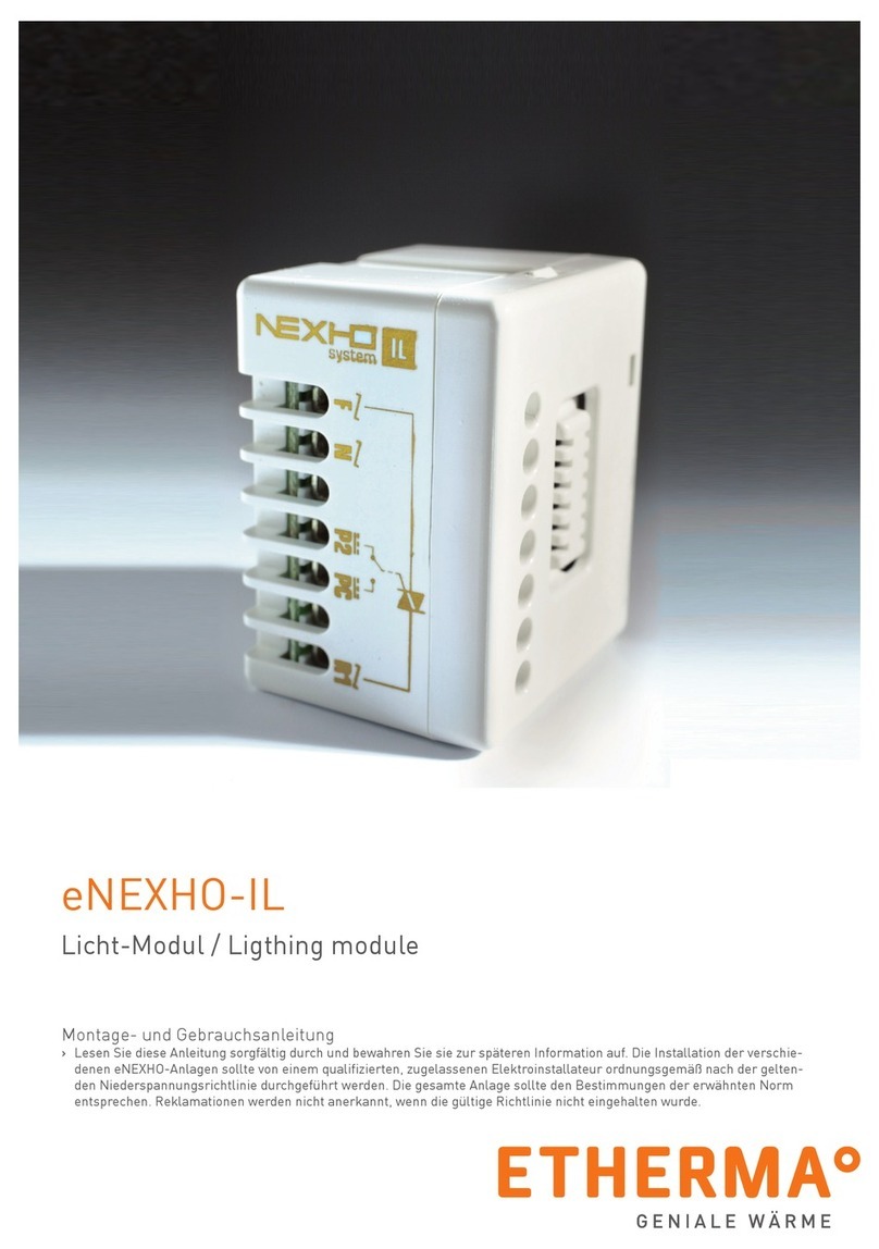
Etherma
Etherma eNEXHO-IL Assembly and operating instructions
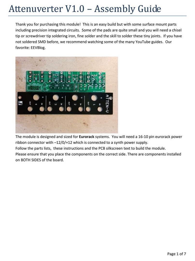
PMFoundations
PMFoundations Attenuverter Assembly guide

GEA
GEA VARIVENT Operating instruction
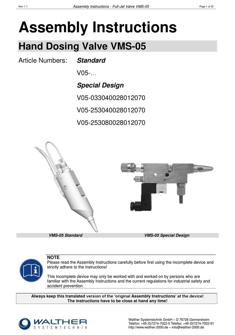
Walther Systemtechnik
Walther Systemtechnik VMS-05 Assembly instructions
Altronix
Altronix LINQ8PD Installation and programming manual

