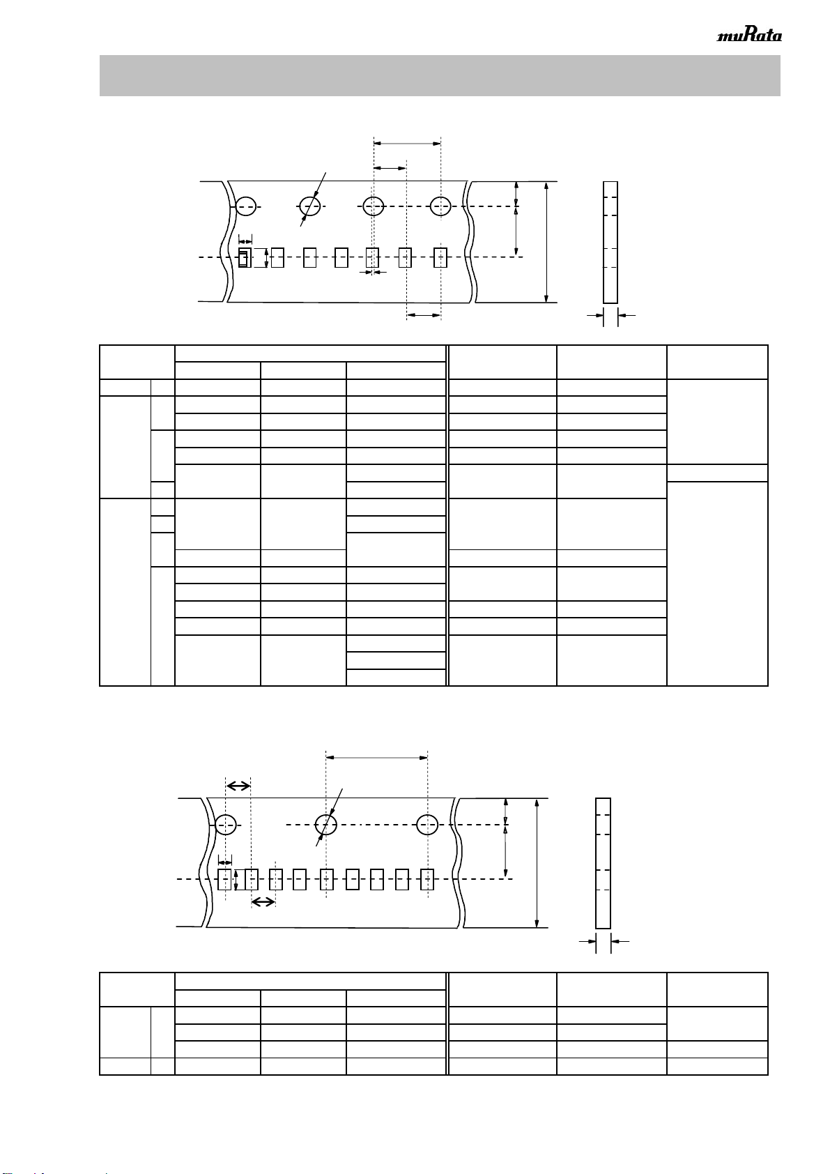
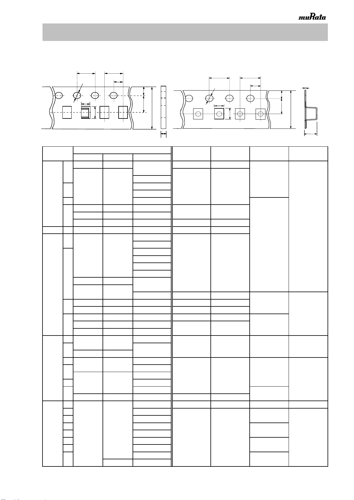
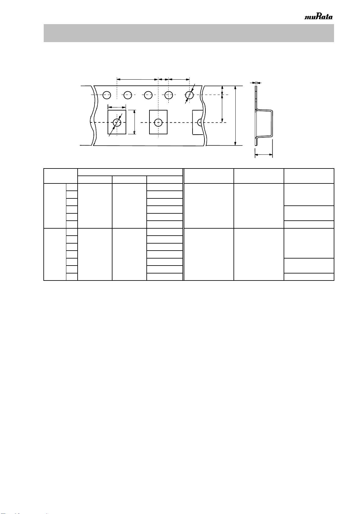
Murata GRM0335C1E681FA01 Series User manual
Other Murata Industrial Electrical manuals

Murata
Murata GRM21BC8YA106KE11 Series User manual

Murata
Murata GRM155R60J823KA01 Series User manual

Murata
Murata GCM188R71H123KA37 Series User manual

Murata
Murata GRT32DC81E106ME01 Series User manual

Murata
Murata GJM0225C1E2R2CB01 Series User manual

Murata
Murata GRM022R61A471MA01 Series User manual

Murata
Murata GQM1555C2D9R1WB01 Series User manual

Murata
Murata GRM319R71H102KA01 Series User manual

Murata
Murata GRM1555C1ER40BA01 Series User manual

Murata
Murata GRM0335C1H5R3BA01 Series User manual

Murata
Murata GRM0225C1E1R8WA03 Series User manual

Murata
Murata GRM0335C1H8R2CA01 Series User manual

Murata
Murata GQM1885C1H120FB01 Series User manual

Murata
Murata GRM0335C1H8R8BA01 Series User manual

Murata
Murata GRM0335C1H510JA01 Series User manual

Murata
Murata GRM1555C2A6R9CA01 Series User manual

Murata
Murata GRM033R71C472KE14 Series User manual

Murata
Murata GRM188R71E682KA01 Series User manual

Murata
Murata GRM033R61A153KE84 Series User manual

Murata
Murata GRM0335C1E3R5CA01 Series User manual


Popular Industrial Electrical manuals by other brands

Rexroth Indramat
Rexroth Indramat DURADRIVE SYSTEM200 Project planning manual

Abtech
Abtech HVJB Series Installation, operation & maintenance instructions

SAF-HOLLAND
SAF-HOLLAND CBX 5415.5 Installation and operation manual

Eaton
Eaton Ulusoy HMH24-04 user manual

Newlong
Newlong NP-7H NSTRUCTION MANUAL/PARTS LIST

Stahl
Stahl 8575/12 operating instructions

SI
SI Pegasus installation instructions

Cooper Power Systems
Cooper Power Systems VXE15 Installation and operation instructions

S&C
S&C Vista SD manual

Siemens
Siemens 3VA9988-0BM10 operating instructions

Siemens
Siemens SITRANS LVS100 operating instructions

Rockwell Automation
Rockwell Automation Allen-Bradley MP-Series installation instructions