Murata GCM1885C1H390FA16D 0603 User manual

GCM1885C1H390FA16_ (0603, C0G, 39pF, 50Vdc)
_: packaging code Reference Sheet
1.Scope
2.MURATA Part NO. System
(Ex.)
3. Type & Dimensions
(Unit:mm)
4.Rated value
5.Package
Product specifications in this catalog are as of Jan.26,2013,and are subject to change or obsolescence without notice.
Please consult the approval sheet before ordering.
Please read rating and !Cautions first.
CHIP MONOLITHIC CERAMIC CAPACITOR FOR AUTOMOTIVE
g
0.2 to 0.5
39 pF
Temp. Range
(Ref.Temp.)
(8) Packaging
mark
(4)
DC Rated
Voltage
Packaging Unit
±1 %
-55 to 125 °C
0±30 ppm/°C
25 to 125 °C
(25 °C)
(3) Temperature Characteristics
(Public STD Code):C0G(EIA)
Specifications and Test
Methods
(Operationg
Temp. Range)
Temp. coeff
or Cap. Change
(5) Nominal
Capacitance
(6)
Capacitance
Tolerance
50 Vdc
0.5 min.
(2) T
0.8±0.1
This product specification is applied to Chip Monolithic Ceramic Capacitor used for Automotive Electronic equipment.
(1)-1 L
1.6±0.1
(1)-2 W
0.8±0.1
e
D
f180mm Reel
PAPER W8P4
4000 pcs./Reel
J
f330mm Reel
PAPER W8P4
10000 pcs./Reel
(1)L/W
Dimensions
(2)T
Dimensions
(3)Temperature
Characteristics
(4)DC Rated
Voltage
(5)Nominal
Capacitance
(6)Capacitance
Tolerance
(8)Packaging
Code
(7)Murata’s
Control Code
T
L
W
e
e
g
GCM 18 85C 1H 390 F A16 D
GCM1885C1H390FA16-01 1

Temperature
Compensating Type High Dielectric Type
Pre-and Post-Stress
Electrical Test
2High Temperature The measured and observed characteristics should satisfy the
Set the capacitor for 1000±12 hours at 150±3℃. Set for
Exposure (Storage) specifications in the following table. 24±2 hours at room temperature, then measure.
Appearance No marking defects
Capacitance Within ±2.5% or ±0.25pF R7/L8/R9: Within ±10.0%
Change (Whichever is larger)
Q/D.F.
30pFmin. : Q≧1000 R7/L8 W.V.: 25Vmin.: 0.03 max.
30pFmax.: Q ≧400+20C W.V.: 16V/10V : 0.05 max.
C: Nominal Capacitance(pF) R9 : 0.075max.
I.R.
More than 10,000MΩor 500Ω・F
(Whichever is smaller)
R9 : More than 150Ω ・F
3 Temperature Cycling The measured and observed characteristics should satisfy the Fix the capacitor to the supporting jig in the same manner and under
specifications in the following table. the same conditions as (19). Perform cycle test according to the four
Appearance No marking defects heat treatments listed in the following table. Set for 24±2 hours at
Capacitance Within ±2.5% or ±0.25pF R7/L8/R9: Within ±10.0% room temperature, then measure
Change (Whichever is larger)
Q/D.F.
30pFmin. : Q≧1000 R7/L8 W.V.: 25Vmin.: 0.03 max.
30pFmax.: Q ≧400+20C W.V.: 16V/10V : 0.05 max.
C: Nominal Capacitance(pF) R9 : 0.05max.
I.R.
More than 10,000MΩor 500Ω・F
(Whichever is smaller)
・Initial measurement for high dielectric constant type
Perform a heat treatment at 150+0/-10 ℃for one hour and then set
for 24±2 hours at room temperature.
Perform the initial measurement.
4 Destructive No defects or abnormalities Per EIA-469.
Phisical Analysis
5 Moisture Resistance The measured and observed characteristics should satisfy the
Apply the 24-hour heat (25 to 65℃) and humidity(80 to 98%)
specifications in the following table.
treatment shown below, 10 consecutive times.
Appearance No marking defects
Set for 24±2 hours at room temperature, then measure.
Capacitance Within ±3.0% or ±0.30pF R7/L8/R9: Within ±12.5%
Change (Whichever is larger)
Q/D.F.
30pFmin. : Q≧350 R7/L8 : W.V.: 25Vmin.: 0.03 max.
10pF and over, 30pF and below: W.V.: 16V/10V : 0.05 max.
Q≧275+5C/2 R9 : 0.075max.
10pFmax.: Q ≧200+10C
C: Nominal Capacitance(pF)
I.R.
More than 10,000MΩor 500Ω・F
(Whichever is smaller)
R9 : More than 150Ω・F
6Biased Humidity The measured and observed characteristics should satisfy the
Apply the rated voltage and 1.3+0.2/-0vdc (add 6.8kΩ resister)
specifications in the following table.
at 85±3℃and 80 to 85% humidity for 1000±12 hours.
Appearance No marking defects
Remove and set for 24±2 hours at room temprature, then measure.
Capacitance Within ±3.0% or ±0.30pF R7/L8/R9: Within ±12.5%
The charge/discharge current is less than 50mA.
Change (Whichever is larger)
Q/D.F.
30pF and over: Q≧200 R7/L8 W.V.: 25Vmin.: 0.035 max.
30pF and below: Q≧100+10C/3 W.V.: 16V/10V : 0.05 max.
C: Nominal Capacitance(pF) R9 : 0.075max.
I.R.
More than 1,000MΩor 50Ω・F
(Whichever is smaller)
■AEC-Q200 Murata Standard Specification and Test Methods
No
AEC-Q200 Test Item
AEC-Q200 Test Method
Specification.
1
-
Step
Time(min)
Cycles
1000(for ΔC/R7)
300(for 5G/L8/R9)
1
15±3
-55℃+0/-3
-55℃+0/-3
2
1
Room
Room
3
15±3
125℃+3/-0
150℃+3/-0
4
1
Room
Room
One cycle 24hours
Hours
Initial measuremt
+10
- 2 ℃
Humidity
90~98%
Humidity
80~98%
Humidity
80~98%
Humidity
90~98%
Humidity
90~98%
0 1 2 3 4 5 6 7 8 9 10 11 12 13 14 15 16 17 18 19 20 21 22 23 24
Temperature
70
65
60
55
50
45
40
35
30
25
20
15
10
5
0
-5
-10
(℃)
JEMCGS-0363S 2

Temperature
Compensating Type
High Dielectric Type
7 Operational Life The measured and observed characteristics should satisfy the
Apply 200% of the rated voltage for 1000±12 hours at 125±3℃(for
specifications in the following table.
ΔC/R7), 150±3℃(for 5G/L8/R9).
Appearance No marking defects
Set for 24±2 hours at room temperature, then measure.
Capacitance Within ±3.0% or ±0.30pF R7/L8/R9: Within ±12.5% The charge/discharge current is less than 50mA.
Change (Whichever is larger)
Q/D.F.
30pFmin. : Q≧350 R7/L8 : W.V.: 25Vmin.: 0.035 max. ・Initial measurement for high dielectric constant type.
10pF and over, 30pF and below: (GCM155R71H 562-223: 0.05max) Apply 200% of the rated DC voltage for one hour at the maximun
Q≧275+5C/2 W.V.: 16V/10V : 0.05 max. operating temperature ±3℃. Remove and set for 24±2 hours at
10pFmax.: Q ≧200+10C R9 : 0.075max. room temperature. Perform initial measurement.
C: Nominal Capacitance(pF)
I.R.
More than 1,000MΩor 50Ω・F
(Whichever is smaller)
8 External Visual No defects or abnormalities Visual inspection
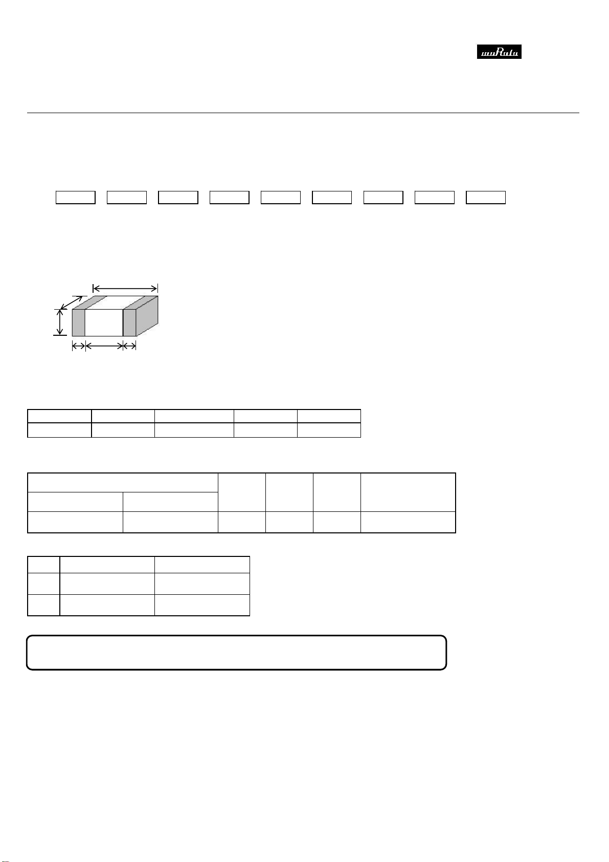
9 Phisical Dimension Within the specified dimensions Using calipers
10 Resistance to Appearance No marking defects
Per MIL-STD-202 Method 215
Solvents Capacitance Within the specified tolerance Solvent 1 : 1 part (by volume) of isopropyl alcohol
Change 3 parts (by volume) of mineral spirits
Q/D.F.
30pFmin. : Q≧1000 R7/L8 : W.V.: 25Vmin.: 0.025 max. Solvent 2 : Terpene defluxer
30pFmax.: Q ≧400+20C W.V.: 16V/10V : 0.035 max. Solvent 3 : 42 parts (by volume) of water
C: Nominal Capacitance(pF) R9 : 0.05max.
1part (by volume) of propylene glycol monomethylether
1 part (by volume) of monoethanolomine
I.R.
More than 10,000MΩor 500Ω・F
(Whichever is smaller)
11 Mechanical Appearance No marking defects
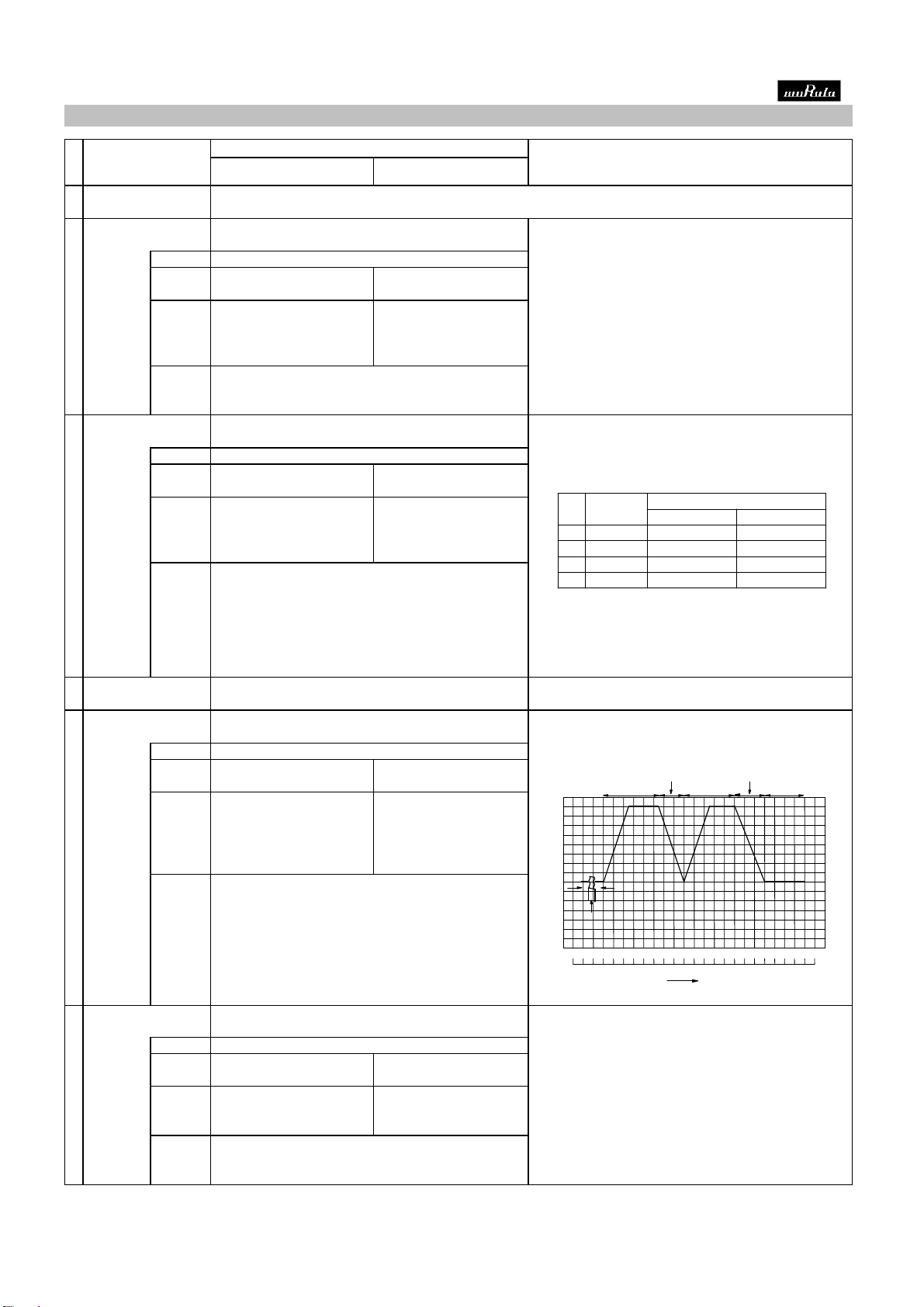
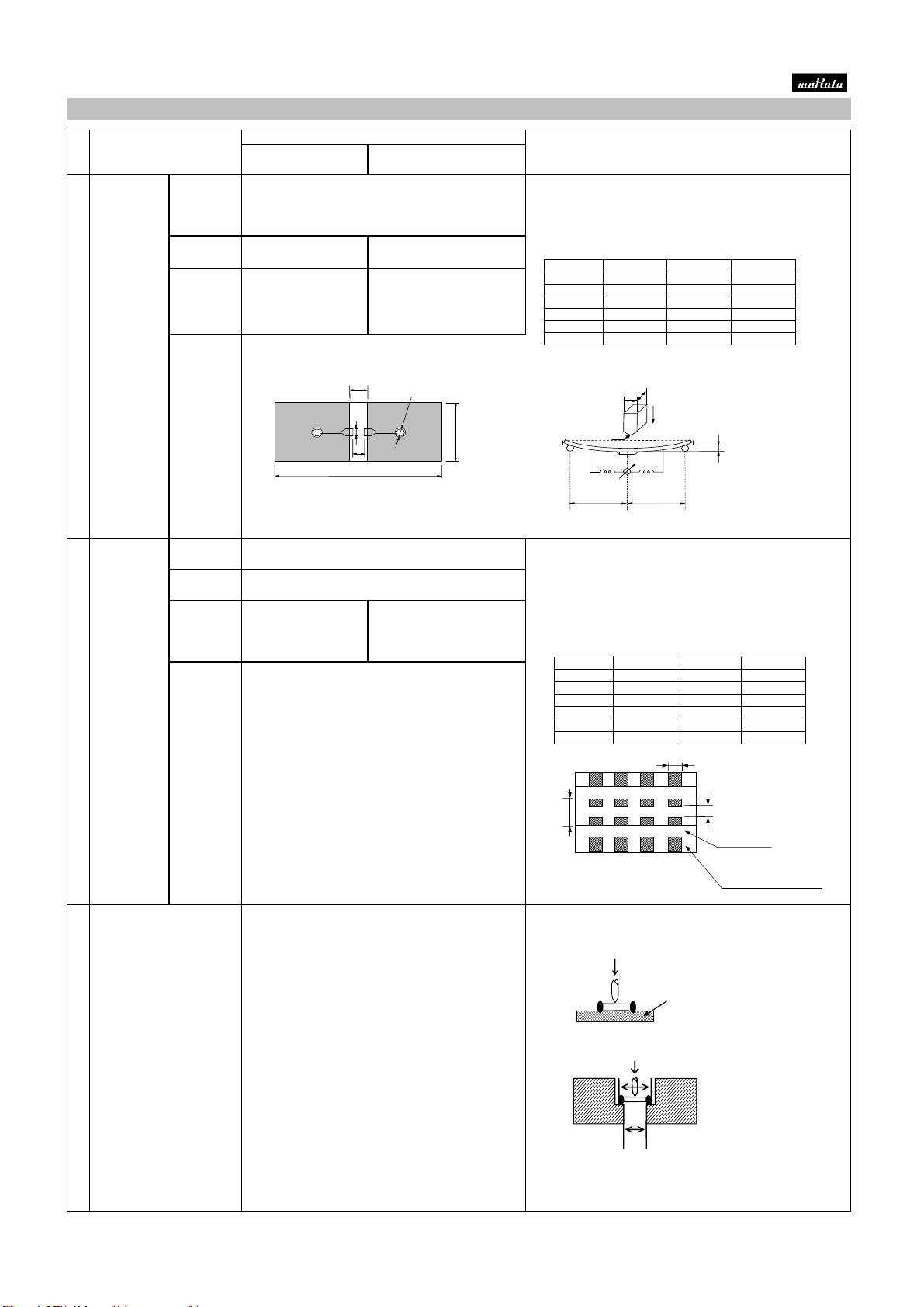
Three shocks in each direction should be applied along 3 mutually
Shock Capacitance Within the specified tolerance
perpendicular axes of the test specimen (18 shocks).
Change
The specified test pulse should be Half-sine and should have a
Q/D.F.
30pFmin. : Q≧1000 R7/L8 : W.V.: 25Vmin.: 0.025 max. duration :0.5ms, peak value:1500g and velocity change: 4.7m/s.
30pFmax.: Q ≧400+20C W.V.: 16V/10V : 0.035 max.
C: Nominal Capacitance(pF) R9 : 0.05max.
I.R.
More than 10,000MΩor 500Ω・F
(Whichever is smaller)
12 Vibration Appearance No defects or abnormalities
Solder the capacitor to the test jig (glass epoxy board) in the same
Capacitance Within the specified tolerance
manner and under the same conditions as (19). The capacitor
Change
should be subjected to a simple harmonic motion having a total
Q/D.F.
30pFmin. : Q≧1000 R7/L8 : W.V.: 25Vmin.: 0.025 max. amplitude of 1.5mm, the frequency being varied uniformly between
30pFmax.: Q ≧400+20C W.V.: 16V/10V : 0.035 max. the approximate limits of 10 and 2000Hz. The frequency range, from
C: Nominal Capacitance(pF) R9 : 0.05max. 10 to 2000Hz and return to 10Hz, should be traversed in
approximately 20 minutes. This motion should be applied for 12
I.R.
More than 10,000MΩor 500Ω・Fitems in each 3 mutually perpendicular directions (total of 36 times).
(Whichever is smaller)
13 Resistance to The measured and observed characteristics should satisfy the
Immerse the capacitor in a eutectic solder solution at 260±5℃for
Soldering Heat specifications in the following table.
10±1 seconds. Set at room temperature for 24±2 hours, then
Appearance No marking defects
measure.
Capacitance Within the specified tolerance
Change
・Initial measurement for high dielectric constant type
Q/D.F.
30pFmin. : Q≧1000 R7/L8 : W.V.: 25Vmin.: 0.025 max. Perform a heat treatment at 150+0/-10 ℃for one hour and then set
30pFmax.: Q ≧400+20C W.V.: 16V/10V : 0.035 max. for 24±2 hours at room temperature.
C: Nominal Capacitance(pF) R9 : 0.05max. Perform the initial measurement.
I.R. More than 10,000MΩor 500Ω・F
(Whichever is smaller)
■AEC-Q200 Murata Standard Specification and Test Methods
No
AEC-Q200 Test Item
AEC-Q200 Test Method
Specification.
JEMCGS-0363S 3

Temperature
Compensating Type High Dielectric Type
14 Thermal Shock The measured and observed characteristics should satisfy the
Fix the capacitor to the supporting jig in the same manner and under
specifications in the following table.
the same conditions as (19). Perform the 300 cycles according to
Appearance No marking defects
the two heat treatments listed in the following table(Maximum
Capacitance Within ±2.5% or ±0.25pF R7/L8/R9: Within ±10.0%
transfer time is 20 seconds). Set for 24±2 hours at room
Change (Whichever is larger)
temperature, then measure
Q/D.F.
30pFmin. : Q≧1000 R7/L8 : W.V.: 25Vmin.: 0.025 max.*
30pFmax.: Q ≧400+20C *0.05max:GCM188R71E/1H563 to 104
C: Nominal Capacitance(pF) W.V.: 16V/10V : 0.035 max.
R9 : 0.05max
I.R.
More than 10,000MΩ or 500Ω・F
(Whichever is smaller)
・Initial measurement for high dielectric constant type
Perform a heat treatment at 150+0/-10 ℃ for one hour and then set
for 24±2 hours at room temperature.
Perform the initial measurement.
15 ESD Appearance No marking defects
Per AEC-Q200-002
Capacitance Within the specified tolerance
Change
Q/D.F.
30pFmin. : Q≧1000 R7/L8 : W.V.: 25Vmin.: 0.025 max.
30pFmax.: Q ≧400+20C W.V.: 16V/10V :0.035 max.
C: Nominal Capacitance(pF) R9 : 0.05max.
I.R.
More than 10,000MΩ or 500Ω・F
(Whichever is smaller)
16 Solderability
(a) Preheat at 155℃for 4 hours. After preheating, immerse the
capacitor in a solution of ethanol(JIS-K-8101) and rosin (JIS-K-
5902) (25% rosin in weight propotion). Immerse in
eutectic solder solution for 5+0/-0.5 seconds at 235±5℃.
(b) should be placed into steam aging for 8 hours±15 minutes.
After preheating, immerse the capacitor in a solution of
ethanol(JIS-K-8101) and rosin (JIS-K-5902) (25% rosin in weight
propotion). Immerse in eutectic solder solution for 5+0/-0.5
seconds at 235±5℃.
(c) should be placed into steam aging for 8 hours±15 minutes.
After preheating, immerse the capacitor in a solution of
ethanol(JIS-K-8101) and rosin (JIS-K-5902) (25% rosin in weight
propotion). Immerse in eutectic solder solution for 120±5
seconds at 260±5℃.
17 Electrical Appearance No defects or abnormalities Visual inspection.
Chatacteri- Capacitance Within the specified tolerance
The capacitance/Q/D.F. should be measured at 25℃at the
zation Change
frequency and voltage shown in the table.
Q/D.F.
30pFmin. : Q≧1000 R7/L8 : W.V.: 25Vmin.: 0.025 max.
30pFmax.: Q ≧400+20C W.V.: 16V/10V : 0.035 max.
C: Nominal Capacitance(pF) R9 : 0.05max.
I.R. 25℃More than 100,000MΩ or 1000Ω・FMore than 10,000MΩ or 500Ω・FThe insulation resistance should be measured with a DC voltage not
(Whichever is smaller) (Whichever is smaller)
exceeding the rated voltage at 25℃and 125℃(for ΔC/R7)/ 150℃
(for 5G/L8/R9)within2 minutes of charging.
I.R. 125℃More than 10,000MΩ or 100Ω・FMore than 1,000MΩ or 10Ω・F
(Whichever is smaller) (Whichever is smaller)
I.R. 150℃More than 10,000MΩ or 100Ω・FMore than 1,000MΩ or 1Ω・F
(Whichever is smaller) (Whichever is smaller)
Dielectric No failure No failure should be observed when 250% of the rated voltage is
Strength applied between the terminations for 1 to 5 seconds, provided the
charge/ discharge current is less than 50mA.
95% of the terminations is to be soldered evenly and continuously.
■AEC-Q200 Murata Standard Specification and Test Methods
No
AEC-Q200 Test Item
AEC-Q200 Test Method
Specification.
Step
1
2
Temp.(℃)
-55+0/-3
125+3/-0(forΔC/R7)
150+3/-0(for 5G/L8/R9)
Time
(min.)
15±3
15±3
Char.
Item
ΔC,5G
(1000 pF and below)
ΔC,5G
(more than 1000pF)
R7,R9,L8(C≦10μF)
Frequency
1±0.1MHz
1±0.1kHz
Voltage
0.5 to 5Vrms
1±0.2Vrms
JEMCGS-0363S 4

Temperature
Compensating Type
High Dielectric Type
18 Board Flex Appearance No marking defects
Solder the capacitor on the test jig (glass epoxy board) shown in
Fig1 using a eutectic solder. Then apply a force in the direction
shown in Fig 2 for 5±1sec. The soldering should be done by the
reflow method and should be conducted with care so that the
Capacitance Within ±5.0% or ±0.5pF R7/L8/R9: Within ±10.0%
soldering is uniform and free of defects such as heat shock.
Change (Whichever is larger)
Q/D.F.
30pFmin. : Q≧1000 R7/L8 : W.V.: 25Vmin.: 0.025 max.
30pFmax.: Q ≧400+20C W.V.: 16V/10V : 0.035max.
C: Nominal Capacitance(pF) R9 : 0.05max.
I.R.
More than 10,000MΩor 500Ω・F
(Whichever is smaller)
19 Terminal Appearance No marking defects Solder the capacitor to the test jig (glass epoxy board) shown in
Strength Fig.3 using a eutectic solder. Then apply *18N force in parallel with
Capacitance Within specified tolerance the test jig for 60sec.
Change The soldering should be done either with an iron or using the reflow
Q/D.F.
30pFmin. : Q≧1000 R7/L8 : W.V.: 25Vmin.: 0.025 max. method and should be conducted with care so that the soldering is
30pFmax.: Q ≧400+20C W.V.: 16V/10V : 0.035max. uniform and gree of defects such as heat shock
C: Nominal Capacitance(pF) R9 : 0.05max.
I.R.
More than 10,000MΩor 500Ω・F
(Whichever is smaller)
(in mm)
20 Beam Load Test Destruction value should be exceed following one. Place the capacitor in the beam load fixture as Fig 4.
< Chip L dimension : 2.5mm max. > Apply a force.
< Chip Length : 2.5mm max. >
< Chip L dimension : 3.2mm max. >
< Chip Length : 3.2mm min. >
Speed supplied the Stress Load : *0.5mm / sec.
*GCM03: 0.1mm/sec.
Chip thickness < 1.25mm rank : 15N
Chip thickness ≧1.25mm rank : 54.5N
Chip thickness > 0.5mm rank : 20N
Chip thickness ≦0.5mm rank : 8N
■AEC-Q200 Murata Standard Specification and Test Methods
No
AEC-Q200 Test Item
AEC-Q200 Test Method
Specification.
t : 1.6mm
Fig.3
Fig.4
*2N(GCM03/15)
(GCM03/15:0.8mm
Type
a
b
c
GCM03
0.3
0.9
0.3
GCM15
0.5
1.5
0.6
GCM18
0.6
2.2
0.9
GCM21
0.8
3.0
1.3
GCM31
2.0
4.4
1.7
GCM32
2.0
4.4
2.6
(in mm)
*2
4.0±0.1
8.0±0.3
3.5±0.05
0.05以下
*1
φ1.5
+0.1
-0
A
t
*1,2:2.0±0.05
1.75±0.1
B
100
40
a
c
b
f4.5
c
Fig.1
Type
a
b
c
GCM03
0.3
0.9
0.3
GCM15
0.4
1.5
0.5
GCM18
1.0
3.0
1.2
GCM21
1.2
4.0
1.65
GCM31
2.2
5.0
2.0
GCM32
2.2
5.0
2.9
*2
4.0±0.1
8.0±0.3
3.5±0.05
0.05以下
*1
φ1.5
+0.1
-0
A
t
*1,2:2.0±0.05
1.75±0.1
B
a
a
c
b
ランド
f4.5
c
Solder resist
Baked electrode or
Copper foil
b
t: 1.6mm
(GCM03/15: 0.8mm)
Iron Board
45
45
Flexure:≦2
(High Dielectric Type)
Capacitance meter
Pressurizing
speed:1.0mm/s
Pressurize
支持台
コンデンサ
45
45
Fig.2
Flexure:≦3
(Temperature
Compensating Type)
R4
20
114
L
0.6L
JEMCGS-0363S 5

Temperature
Compensating Type High Dielectric Type
21 Capacitance Capacitance Within the specified tolerance. R7 : Within ±15% The capacitance change should be measured after 5 min. at
Temperature Change (Table A) (-55℃to +125℃)each specified temperature stage.
Characteristics L8 : Within ±15% (1)Temperature Compensating Type
(-55℃to +125℃) The temperature coefficient is determind using the capacitance
Within +15/-40% measured in step 3 as a reference. When cycling the temperature
(+125℃to +150℃)sequentially from step1 through 5 (ΔC: +25℃to +125℃,
R9 : Within ±15% 5G:+25℃to +150℃other temp. coeffs.:+25℃to +85℃) the
(-55℃to +150℃)capacitance should be within the specified tolerance for the
temperature coefficient and capacitance change as Table A-1. The
capacitance drift is caluculated by dividing the differences
betweeen the maximum and minimum measured values in the step
Temperature Within the specified tolerance. 1,3 and 5 by the cap value in step 3.
Coefficent (Table A)
Capacitance
Within ±0.2% or ±0.05 pF
Drift (Whichever is larger.) (2) High Dielectric Constant Type
The ranges of capacitance change compared with the above 25℃
value over the temperature ranges shown in the table should be
within the specified ranges.
Initial measurement for high dielectric constant type.
Perform a heat treatment at 150+0/-10℃for one hour
and then set for 24±2 hours at room temperature.
Perform the initial measurement.
■AEC-Q200 Murata Standard Specification and Test Methods
No
AEC-Q200 Test Item
AEC-Q200 Test Method
Specification.
Step
Temperature.(C)
1
25±2
2
-55±3(for ΔC to R7)
3
25±2
4
125±3(for ΔC/R7), 150±3(for 5G/R9/L8),85±3(for other TC)
5
25±2
Table A
Char.
Nominal Values
(ppm/C)
Capacitance Change from 25C (%)
-55
-30
-10
Max.
Min.
Max.
Min.
Max.
Min.
5C/5G
0±30
0.58
-0.24
0.40
-0.17
0.25
-0.11
Note1: Nominalvaluesdenotethetemperaturecoefficientwithinarangeof25Cto125C(forC)/150C(for5G)/85C(forotherTC).
JEMCGS-0363S 6

1.Tape Carrier Packaging(Packaging Code:D/E/W/F/L/J/K)
1.1 Minimum Quantity(pcs./reel)
φ180mm reel φ330mm reel
Plastic Tape Paper Tape Plastic Tape
Code:D/E Code:W Code:L Code:J/ F Code:K
GC□03 15000(W8P2) 30000(W8P1) 50000(W8P2)
GC□15 10000(W8P2) 20000(W8P1) 50000(W8P2)
GC□18 4000 10000
64000 10000
94000 10000
B3000 10000
64000 10000
94000 10000
M3000 10000
C2000 6000
94000 10000
M3000 10000
N2000 8000
R/D/E 1000 4000
M1000 5000
N/R 1000 4000
E500 2000
M1000 5000
N/R 1000 4000
1.2 Dimensions of Tape
(1)GC□03/15(W8P2 CODE:D/E/J/F) (in:mm)
Code GC□03 GC□15
A *3 0.37 0.65
B *3 0.67 1.15 *3 Nominal value
t0.5 max. 0.8 max.
(2)GC□03/15(W8P1 CODE:W) (in:mm)
Code GC□03 GC□15
A * 0.37 0.65
B * 0.67 1.15 * Nominal value
t0.5 max. 0.8 max.
Package
GC□ Type
GC□55
Paper Tape
Type
GC□21
GC□31
GC□32
GC□43
*1,2:2.0±0.05
*2
4.0±0.1
8.0±0.3
3.5±0.05
0.05以下
*1
φ1.5
+0.1
-0
A
t
*1,2:2.0±0.05
1.75±0.1
B
4.0±0.1
*1
φ1.5
+0.1
-0
1.75±0.1
8.0±0.3
3.5±0.05
A
B
t
*2
0.05 max.
1.0±0.05
4.0±0.1
φ1.5
+0.1
-0
1.75±0.1
8.0±0.3
3.5±0.05
A
B
t
1.0±0.05
JEMCGP-01894A 7

(3)GC□18/21/31/32 T:0.85 rank max. (in:mm)
Code GC□18 GC□21 GC□31 GC□32
A 1.05±0.1 1.55±0.15 2.0±0.2 2.8±0.2
B 1.85±0.1 2.3±0.15 3.6±0.2 3.6±0.2
(4)GC□21/31/32 T:1.15 rank min. (in:mm)
Code GC□21 GC□31 GC□32
A 1.45±0.2 1.9±0.2 2.8±0.2
B 2.25±0.2 3.5±0.2 3.5±0.2
(5)GC□43/55 (in:mm)
Code GC□43 GC□55
A *2 3.6 5.2 *2 Nominal value
B *2 4.9 6.1
Package
GC□ Type
4.0±0.1
4.0±0.1
2.0±0.1
φ1.5
+0.1
-0
1.75±0.1
8.0±0.3
3.5±0.05
1.1 max.
A
B
8.0±0.3
4.0±0.1
3.5±0.05
1.75±0.1
A
B
*
2.0±0.1
φ1.5
+0.1
-0
*
1.7 max.(T≦1.25mm)
2.5 max. (T:1.35/1.6mm)
3.0 max. (T:1.8/2.0mm)
3.7 max. (T≧2.5mm)
4.0±0.1
0.25±0.1(T≦2.0mm)
0.3±0.1(T:2.5mm)
φ1.5
+0.1
-0
4.0±0.1
8.0±0.1
φ1.5
+0.2
-0
12.0±0.3
5.5±0.1
1.75±0.1
A
*
*1
2.5 max.(T≦1.8mm)
B
*1
*:2.0±0.1
0.3±0.1
JEMCGP-01894A 8

Package
GC□ Type
図
1
チップ詰め状態
(
単位:
mm)
φ21±0.8
w1
W
Top Tape : Thickness 0.06
Feeding Hole :As specified in 1.2.
Hole for Chip : As specified in 1.2.
Base Tape : As specified in 1.2.
Bottom Tape :Thickness 0.05
(Only a bottom tape existence )
W
w1
GC□32 max.
16.5 max.
10±1.5
GC□43/55
20.5 max.
14±1.5
φ180+0/-3.0
φ330±2.0
φ50 min.
φ13±0.5
2.0±0.5
Chip
(in:mm)
Fig.1 Package Chips
Fig.2 Dimensions of Reel
Fig.3 Taping Diagram
JEMCGP-01894A 9

1.3 Tapes for capacitors are wound clockwise shown in Fig.3.
(The sprocket holes are to the right as the tape is pulled toward the user.)
1.4 Part of the leader and part of the vacant section are attached as follows.
(in:mm)
1.5 Accumulate pitch : 10 of sprocket holes pitch = 40±0.3mm
1.6 Chip in the tape is enclosed by top tape and bottom tape as shown in Fig.1.
1.7 The top tape and base tape are not attached at the end of the tape for a minimum of 5 pitches.
1.8 There are no jointing for top tape and bottom tape.
1.9 There are no fuzz in the cavity.
1.10 Break down force of top tape : 5N min.
Break down force of bottom tape : 5N min.(Only a bottom tape existence )
1.11 Reel is made by resin and appeaser and dimension is shown in Fig 2. There are possibly
to change the material and dimension due to some impairment.
1.12 Peeling off force : 0.1N to 0.6N*in the direction as shown below.
* GC□03:0.05N~0.5N
1.13 Label that show the customer parts number, our parts number, our company name, inspection
number and quantity, will be put in outside of reel.
Package
GC□ Type
図
1
チップ詰め状態
(
単位:
mm)
Tail vacant Section
Chip-mounting Unit
Leader vacant Section
Leader Unit
(Top Tape only)
Direction
of Feed
160 min.
190 min.
210 min.
図
1
チップ詰め状態
(
単位:
mm)
165~180°
Top tape
JEMCGP-01894A 10

Caution
■ Limitation of use
Please contact our sales representatives or product engineers before using our products for the applications
listed below which require of our products for other applications than specified in this product.
①Aircraft equipment ②Aerospace equipment ③Undersea equipment ④Power plant control equipment
⑤Medical equipment ⑥Transportation equipment(vehicles,trains,ships,etc.) ⑦Traffic signal equipment
⑧Disaster prevention / crime prevention equipment ⑨Data-processing equipment
⑩Application of similar complexity and/or requirements to the applications listed in the above
■Fail-safe
Be sure to provide an appropriate fail-safe function on your product to prevent a second damage that may
be caused by the abnormal function or the failure of our product.
■Storage and Operation condition
1. The performance of chip monolithic ceramic capacitors may be affected by the storage conditions.
1-1. Store capacitors in the following conditions: Temperature of +5℃to +40℃and a Relative Humidity
of 20% to 70%.
(1) Sunlight, dust, rapid temperature changes, corrosive gas atmosphere or high temperature and humidity
conditions during storage may affect the solderability and the packaging performance.
Please use product within six months of receipt.
(2) Please confirm solderability before using after six months.
Store the capacitors without opening the original bag.
Even if the storage period is short, do not exceed the specified atmospheric conditions.
1-2. Corrosive gas can react with the termination (external) electrodes or lead wires of capacitors, and result
in poor solderability. Do not store the capacitors in an atmosphere consisting of corrosive gas (e.g.,
hydrogen sulfide, sulfur dioxide, chlorine, ammonia gas etc.).
1-3. Due to moisture condensation caused by rapid humidity changes, or the photochemical change caused
by direct sunlight on the terminal electrodes and/or the resin/epoxy coatings, the solderability and
electrical performance may deteriorate. Do not store capacitors under direct sunlight or in high huimidity
conditions
!
JEMCGC-2702N 11

■Rating
1.Temperature Dependent Characteristics
1. The electrical characteristics of the capacitor can change with temperature.
1-1. For capacitors having larger temperature dependency, the capacitance may change with temperature
changes. The following actions are recommended in order to insure suitable capacitance values.
(1) Select a suitable capacitance for the operating temperature range.
(2) The capacitance may change within the rated temperature.
When you use a high dielectric constant type capacitors in a circuit that needs a tight (narrow) capacitance
tolerance.
Example: a time constant circuit., please carefully consider the characteristics of these capacitors,
such as their aging, voltage, and temperature characteristics.
And check capacitors using your actual appliances at the intended environment and operating conditions.
□Typical temperature characteristics Char.R6 (X5R) □Typical temperature characteristics Char.R7 (X7R)
□Typical temperature characteristics Char.F5 (Y5V)
2.Measurement of Capacitance
1. Measure capacitance with the voltage and the frequency specified in the product specifications.
1-1. The output voltage of the measuring equipment may decrease when capacitance is high occasionally.
Please confirm whether a prescribed measured voltage is impressed to the capacitor.
1-2. The capacitance values of high dielectric constant type capacitors change depending on the AC voltage
applied. Please consider the AC voltage characteristics when selecting a capacitor to be used in a AC circuit.
Caution
-20
-15
-10
-5
0
5
10
15
20
-75 -50 -25 025 50 75 100
Capacitance Change (%)
Temperature (℃)
-100
-80
-60
-40
-20
0
20
40
-50 -25 025 50 75 100
Capacitance Change (%)
Temperature (℃)
!
JEMCGC-2702N 12

3.Applied Voltage
1. Do not apply a voltage to the capacitor that exceeds the rated voltage as called-out in the specifications.
1-1. Applied voltage between the terminals of a capacitor shall be less than or equal to the rated voltage.
(1) When AC voltage is superimposed on DC voltage, the zero-to-peak voltage shall not exceed the rated
DC voltage. When AC voltage or pulse voltage is applied, the peak-to-peak voltage shall not exceed
the rated DC voltage.
(2) Abnormal voltages (surge voltage, static electricity, pulse voltage, etc.) shall not exceed the rated DC
voltage.
Typical voltage applied to the DC capacitor
DC voltage DC voltage+AC AC voltage Pulse voltage
(E:Maximum possible applied voltage.)
1-2. Influence of overvoltage
Overvoltage that is applied to the capacitor may result in an electrical short circuit caused by the
breakdown of the internal dielectric layers .
The time duration until breakdown depends on the applied voltage and the ambient temperature.
4. Applied Voltage and Self-heating Temperature
1. When the capacitor is used in a high-frequency voltage, pulse voltage, application, be sure to take into account
self-heating may be caused by resistant factors of the capacitor.
1-1. The load should be contained to the level such that when measuring at atomospheric temperature of 25℃,
the product's self-heating remains below 20℃and surface temperature of the capacitor in the actual circuit
remains wiyhin the maximum operating temperature.
Caution
E E E E
0 0
0
0
!
JEMCGC-2702N 13

5. DC Voltage and AC Voltage Characteristic
1. The capacitance value of a high dielectric constant type capacitor changes depending on the DC voltage applied.
Please consider the DC voltage characteristics when a capacitor is selected for use in a DC circuit.
1-1. The capacitance of ceramic capacitors may change sharply depending on the applied voltage. (See figure)
Please confirm the following in order to secure the capacitance.
(1) Whether the capacitance change caused by the
applied voltage is within the range allowed or not.
□DC voltage characteristics
(2) In the DC voltage characteristics, the rate of capacitance
change becomes larger as voltage increases.
Even if the applied voltage is below the rated voltage.
When a high dielectric constant type capacitor is in a
circuit that needs a tight (narrow) capacitance tolerance.
Example: a time constant circuit., please carefully
consider the characteristics of these capacitors, such as
their aging, voltage, and temperature characteristics.
And check capacitors using your actual appliances at the
intended environment and operating conditions.
2. The capacitance values of high dielectric constant type capacitors change depending on the AC voltage applied.
Please consider the AC voltage characteristics when selecting a capacitor to be used in a AC circuit.
□AC voltage characteristics
6. Capacitance Aging
1. The high dielectric constant type capacitors have the characteristic in which the capacitance value decreases
with the passage of time.
When you use a high dielectric constant type capacitors in a circuit that needs a tight (narrow) capacitance
tolerance. Example: a time constant circuit., please carefully consider the characteristics of these capacitors,
such as their aging, voltage, and temperature characteristics.
And check capacitors using your actual appliances at the intended environment and operating conditions.
Caution
-60
-50
-40
-30
-20
-10
0
10
20
30
0.0 0.5 1.0 1.5 2.0 2.5
Capacitance Change (%)
AC Voltage (Vr.ms.)
-100
-80
-60
-40
-20
0
20
02468
Capacitance Change(%)
DC Voltage (VDC)
!
JEMCGC-2702N 14

7.Vibration and Shock
1. The capacitors mechanical actress (vibration and shock) shall be specified for the use environment.
Please confirm the kind of vibration and/or shock, its condition, and any generation of resonance.
Please mount the capacitor so as not to generate resonance, and do not allow any impact on the
terminals.
2. Mechanical shock due to falling may cause damage or a crack in the dielectric material of the capacitor.
Do not use a fallen capacitor because the quality and reliability may be deteriorated.
3. When printed circuit boards are piled up or handled, the corners of another printed circuit board
should not be allowed to hit the capacitor in order to avoid a crack or other damage to the capacitor.
■Soldering and Mounting
1.Mounting Position
1. Confirm the best mounting position and direction that minimizes the stress imposed on the capacitor
during flexing or bending the printed circuit board.
1-1.Choose a mounting position that minimizes the stress imposed on the chip during flexing or bending
of the board.
[Component Direction]
Locate chip horizontal to the
direction in which stress acts
[Chip Mounting Close to Board Separation Point]
Chip arrangement
Worst A-C-(B~D) Best
Caution
Floor
Crack
Mounting printed circuit board
Crack
!
A
B
C
D
Perforation
Slit
JEMCGC-2702N 15

2.Information before mounting
1. Do Not re-use capacitors that were removed from the equipment.
2. Confirm capacitance characteristics under actual applied voltage.
3. Confirm the mechanical stress under actual process and equipment use.
4. Confirm the rated capacitance, rated voltage and other electrical characteristics before assembly.
5. Prior to use, confirm the Solderability for the capacitors that were in long-term storage.
6. Prior to measuring capacitance, carry out a heat treatment for capacitors that were in long-term storage.
7.The use of Sn-Zn based solder will deteriorate the reliability of the MLCC.
Please contact our sales representative or product engineers on the use of Sn-Zn based solder in
advance.
3.Maintenance of the Mounting (pick and place) Machine
1. Make sure that the following excessive forces are not applied to the capacitors.
1-1. In mounting the capacitors on the printed circuit board, any bending force against them shall be kept
to a minimum to prevent them from any bending damage or cracking. Please take into account the
following precautions and recommendations for use in your process.
(1) Adjust the lowest position of the pickup nozzle so as not to bend the printed circuit board.
(2) Adjust the nozzle pressure within a static load of 1N to 3N during mounting.
[Incorrect]
[Correct]
2.Dirt particles and dust accumulated between the suction nozzle and the cylinder inner wall prevent
the nozzle from moving smoothly. This imposes greater force upon the chip during mounting,
causing cracked chips. Also the locating claw, when worn out, imposes uneven forces on the chip
when positioning, causing cracked chips. The suction nozzle and the locating claw must be maintained,
checked and replaced periodically.
Caution
Suction Nozzle
Board Deflection
Support Pin
Board Guide
!
JEMCGC-2702N 16

4-1.Reflow Soldering
1. When sudden heat is applied to the components, the [Standard Conditions for Reflow Soldering]
mechanical strength of the components will decrease
because a sudden temperature change causes Infrared Reflow
deformation inside the components. In order to prevent
mechanical damage to the components, preheating is
required for both the components and the PCB board.
Preheating conditions are shown in table 1. It is required to
keep the temperature differential between the solder and
the components surface (ΔT) as small as possible.
2. Solderability of Tin plating termination chips might be
deteriorated when a low temperature soldering profile where
the peak solder temperature is below the melting point of
Tin is used. Please confirm the Solderability of Tin plated
termination chips before use. Vapor Reflow
3. When components are immersed in solvent after mounting,
be sure to maintain the temperature difference (ΔT)
between the component and the solvent within the range
shown in the table 1.
Table 1
GC□03/15/18/21/31
[Allowable Soldering Temperature and Time]
GC□32
Recommended Conditions
Infrared Reflow Vapor Reflow
Peak Temperature
230~250℃230~240℃240~260℃
Atmosphere Air Air Air or N2
Pb-Sn Solder: Sn-37Pb Lead Free Solder: Sn-3.0Ag-0.5Cu In case of repeated soldering, the accumulated
soldering time must be within the range shown above.
4. Optimum Solder Amount for Reflow Soldering
4-1. Overly thick application of solder paste results in
a excessive solder fillet height.
This makes the chip more susceptible to mechanical
and thermal stress on the board and may cause
the chips to crack.
* GC□03: 1/3 of Chip Thickness min.
4-2. Too little solder paste results in a lack of adhesive in section
strength on the outer electrode, which may result in
chips breaking loose from the PCB.
4-3. Make sure the solder has been applied smoothly to the end surface to a height of 0.2mm* min.
Make sure not to impose any abnormal mechanical shocks to the PCB.
Inverting the PCB
Caution
Part Number
Temperature Differential
ΔT≦190℃
ΔT≦130℃
Pb-Sn Solder
Lead Free Solder
0.2mm* min.
!
Soldering
Soldering
60-120 seconds
60-120 seconds
30-60 seconds
20 seconds
Soldering Temperature(℃)
280
270
260
250
240
230
220
Time
Time
Temperature(℃)
Peak Temperature
200℃
170℃
150℃
130℃
Gradual
Cooling
Temperature(℃)
Peak Temperature
170℃
150℃
130℃
Gradual
Cooling
0
30
60
90
120
Soldering Time(sec.)
Preheating
Preheating
JEMCGC-2702N 17

4-2.Flow Soldering
1. When sudden heat is applied to the components, the [Standard Conditions for Flow Soldering]
mechanical strength of the components will decrease
because a sudden temperature change causes
deformation inside the components. In order to prevent
mechanical damage in the components, preheating should
be required for both of the components and the PCB board.
Preheating conditions are shown in table 2. It is required to
keep temperature differential between the solder and
the components surface (ΔT) as small as possible.
2. Excessively long soldering time or high soldering
temperature can result in leaching of the outer electrodes,
causing poor adhesion or a reduction in capacitance value
due to loss of contact between electrodes and end termination.
[Allowable Soldering Temperature and Time]
3. When components are immersed in solvent after mounting,
be sure to maintain the temperature difference (ΔT)
between the component and solvent within the range
shown in the table 2.
4. Do not apply flow soldering to chips not listed in Table 2.
Table 2
In case of repeated soldering, the accumulated
soldering time must be within the range shown above.
Recommended Conditions Pb-Sn Solder Lead Free Solder
90~110℃100~120℃
240~250℃250~260℃
Air
N2
Pb-Sn Solder: Sn-37Pb Lead Free Solder: Sn-3.0Ag-0.5Cu
5. Optimum Solder Amount for Flow Soldering
5-1. The top of the solder fillet should be lower than the
thickness of components. If the solder amount is
excessive, the risk of cracking is higher during
board bending or any other stressful condition. in section
Caution
Preheating Peak Temperature
Soldering Peak Temperature
Atmosphere
Part Number
GC□18/21/31
Temperature Differential
ΔT≦150℃
Up to Chip Thickness
Adhesive
!
Temperature(℃)
Soldering Peak
Temperature
Preheating Peak
Soldering
Gradual
Cooling
Preheating
△T
30-90 seconds
5 seconds max.
Time
280
270
260
240
230
220
250
Soldering Temperature(℃)
0
30
60
90
120
Soldering Time(sec.)
JEMCGC-2702N 18

4-3.Correction with a Soldering Iron
1. When sudden heat is applied to the components when using a soldering iron, the mechanical strength of
the components will decrease because the extreme temperature change can cause deformations inside the
components. In order to prevent mechanical damage to the components, preheating is required for both
the components and the PCB board. Preheating conditions, (The "Temperature of the Soldering Iron tip",
"Preheating Temperature", "Temperature Differential" between the iron tip and the components and the
PCB), should be within the conditions of table 3. It is required to keep the temperature differential
between the soldering Iron and the component surfaces (ΔT) as small as possible.
2. After soldering, do not allow the component/PCB to rapidly cool down.
3. The operating time for the re-working should be as short as possible. When re-working time is too long,
it may cause solder leaching, and that will cause a reduction in the adhesive strength of the terminations.
Table 3
*Applicable for both Pb-Sn and Lead Free Solder.
Pb-Sn Solder: Sn-37Pb
Lead Free Solder: Sn-3.0Ag-0.5Cu
4. Optimum Solder amount when re-working with a Soldering lron
4-1. In case of sizes smaller than 0603, (GC□03/15/18),
the top of the solder fillet should be lower than 2/3's
of the thickness of the component or 0.5mm whichever
is smaller. In case of 0805 and larger sizes, (GC□21/
31/32), the top of the solder fillet should be lower
than 2/3's of the thickness of the component. If the in section
solder amount is excessive, the risk of cracking is higher
during board bending or under any other stressful condition.
4-2. A Soldering iron with a tip of ø3mm or smaller should be used. It is also necessary to keep the soldering
iron from touching the components during the re-work.
4-3. Solder wire with ø0.5mm or smaller is required for soldering.
4-4.Leaded Component Insertion
1. If the PCB is flexed when leaded components (such as transformers and ICs) are being mounted,
chips may crack and solder joints may break.
Before mounting leaded components, support the PCB using backup pins or special jigs to prevent warping.
Caution
150℃min.
ΔT≦190℃
Air
Part Number
Temperature
of Soldering
Iron tip
ΔT≦130℃
Air
Preheating
Temperature
GC□03/15/18/21/31
Temperature
Differential
(ΔT)
Atmosphere
GC□32
280℃max.
150℃min.
350℃max.
Solder Amount
!
JEMCGC-2702N 19

5.Washing
Excessive ultrasonic oscillation during cleaning can cause the PCBs to resonate, resulting in cracked
chips or broken solder joints. Take note not to vibrate PCBs.
6.Electrical Test on Printed Circuit Board
1. Confirm position of the support pin or specific jig, when inspecting the electrical performance of
a capacitor after mounting on the printed circuit board.
1-1. Avoid bending printed circuit board by the pressure of a test pin, etc.
The thrusting force of the test probe can flex the PCB, resulting in cracked chips or open solder joints.
Provide support pins on the back side of the PCB to prevent warping or flexing.
1-2. Avoid vibration of the board by shock when a test pin contacts a printed circuit board.
□Not recommended □Recommended
Caution
←Support pin
←Test-pin
←Peeling
←Test-pin
!
JEMCGC-2702N 20
This manual suits for next models
3
Table of contents
Other Murata Industrial Equipment manuals

Murata
Murata GRM0225C1E6R9CDAE User manual

Murata
Murata GRM0335C1H3R9BA01 User manual

Murata
Murata PRG15 User manual

Murata
Murata GRM0225C1E8R2BDAE User manual

Murata
Murata XBSC Series User manual

Murata
Murata GRM0225C1E8R4BDAE User manual

Murata
Murata LLA219C70G475ME01 Series User manual

Murata
Murata SCC1000 Series User manual
Popular Industrial Equipment manuals by other brands

Kitagawa
Kitagawa TT182BM-22 instruction manual

Meritor
Meritor MORH2P035 Series quick start guide

Texas
Texas EZ Torque Operation manual

Festo
Festo DHTG operating instructions

Ametek
Ametek Gemco 1995A Series Installation & programming manual

John Crane
John Crane 32 Installation, operation & maintenance instructions