Murata LLA219C70G475ME01 Series User manual

CHIP MONOLITHIC CERAMIC CAPACITOR
LLA219C70G475ME01_ (0805, X7S, 4.7uF, 4Vdc)
_: packaging code Reference Sheet
1.Scope
2.MURATA Part NO. System
(Ex.)
3. Type & Dimensions
(Unit:mm)
4.Rated value
5.Package
Product specifications in this catalog are as of Feb.22,2012,and are subject to change or obsolescence without notice.
Please consult the approval sheet before ordering.
Please read rating and !Cautions first.
(8) Packaging
This product specification is applied to Low ESL Chip Monolithic Ceramic Capacitor used for General Electronic equipment.
±20 %
-55 to 125 °C
-22 to 22 %
-55 to 125 °C
(25 °C)
(3) Temperature Characteristics
(Public STD Code):F(EIA)
p
Specifications and Test
Methods
(Operationg
Temp. Range)
Temp. coeff
or Cap. Change
(5) Nominal
Capacitance
(6)
Capacitance
Tolerance
4 Vdc
4.7 uF
Temp. Range
(Ref.Temp.)
mark
0.85±0.1
(4)
DC Rated
Voltage
0.5±0.05
(1)-2 W
1.25±0.1
(2) T
Packaging Unit
(1)-1 L
2.0±0.1
B
Bulk Bag
1000 pcs./Bag
L
f180mm Reel
EMBOSSED
3000 pcs./Reel
K
f330mm Reel
EMBOSSED
10000 pcs./Reel
(1)L/W
Dimensions
(2)T
Dimensions
(3)Temperature
Characteristics
(4)DC Rated
Voltage
(5)Nominal
Capacitance
(6)Capacitance
Tolerance
(8)Packaging
Code
(7)Murata’s
Control Code
L
P
T
W
LLA 21 9C7 0G 475 M E01 L
LLA219C70G475ME01-01 1

No Item Test Method
1 Operating
R7 / C7:-55℃to +125℃
Temperature Range
2 Rated Voltage See the previous pages. The rated voltage is defined as the maximum voltage which may be
applied continuously to the capacitor.
When AC voltage is superimposed on DC voltage, VP-P or VO-P,
whichever is larger, should be maintained within the rated
voltage range.
3 Appearance No defects or abnormalities. Visual inspection.
4 Dimension Within the specified dimensions. Using calipers.
5 Dielectric Strength No defects or abnormalities. No failure shall be observed when 250% of the rated voltage is
applied between the terminations for 1 to 5 seconds, provided the
charge/discharge current is less than 50mA.
6 Insulation
50Ω・F min. The insulation resistance shall be measured with a DC voltage
Resistance
not exceeding the rated voltage at 25℃and 75%RH max. and
within 1 minutes of charging.
7 Capacitance Within the specified tolerance.
The capacitance/D.F. shall be measured at 25℃at the
frequency and voltage shown in the table.
8 Dissipation Factor 0.120max.
(D.F.)
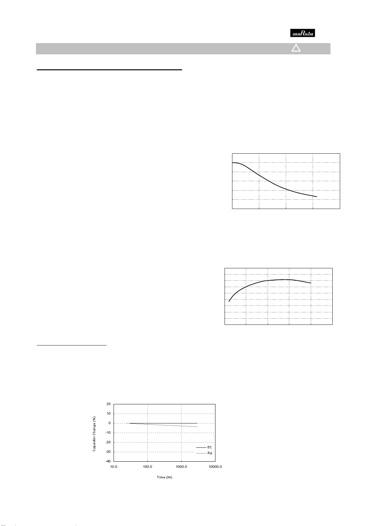
9 Capacitance The capacitance change shall be measured after 5 min. at
Temperature each specified temperature stage.
Characteristics
The ranges of capacitance change compared with the 25℃value
over the temperature ranges shown in the table shall be within
the specified ranges.
10 Adhesive Strength of No removal of the terminations or other defect Solder the capacitor to the test jig (glass epoxy board) using a
Termination should occur. eutectic solder. Then apply 5N force in parallel with the test
jig for 10±1 sec. The soldering shall be done either with an
iron or using the reflow method and shall be conducted with
care so that the soldering is uniform and free of defects such as
heat shock.
11 Vibration Appearance No defects or abnormalities.
Solder the capacitor to the test jig (glass epoxy board) in the same
Resistance manner and under the same conditions as (10). The capacitor shall
Capacitance Within the specified tolerance. be subjected to a simple harmonic motion having a total amplitude
of 1.5mm, the frequency being varied uniformly between the approximate
D.F. 0.120max.
limits of 10 and 55Hz. The frequency range, from 10 to 55Hz and return
to 10Hz, shall be traversed in approximately 1 minute.
This motion shall be applied for a period of 2 hours in each 3 mutually
perpendicular directions (total of 6 hours).
12 Solderability
75% of the terminations is to be soldered evenly
Immerse the capacitor in a solution of ethanol (JIS-K-8101) and
of Termination and continuously. rosin (JIS-K-5902) (25% rosin in weight proportion). Preheat at
80 to 120℃for 10 to 30 seconds. After preheating, immerse in
eutectic solder solution for 2±0.5 seconds at 230±5℃,or
Sn-3.0Ag-0.5Cu solder solution for 2±0.5 seconds at 245±5℃.
■SPECIFICATIONS AND TEST METHODS
Specification
Capacitance
Frequency
Voltage
C≦10μF(10V min.)
1±0.1kHz
1.0±0.2Vrms
C≦10μF(6.3V max.)
1±0.1kHz
0.5±0.1Vrms
C>10μF
120±24Hz
0.5±0.1Vrms
Step
Temperature(C)
1
25±2
2
-55±3
3
25±2
4
125±3
5
25±2
Char.
Temp.Range
(℃)
Reference
Temp.
Cap.Change
R7
-55 to +125
25℃
Within ±15%
C7
-55 to +125
25℃
Within ±22%
JEMCAS-00669A 2

No Item Test Method
13
Temperature Appearance No marking defects. Fix the capacitor to the supporting jig in the same manner and under
Sudden the same conditions as (10). Perform the five cycles according to the
Change Capacitance Within ±12.5% four heat treatments listed in the following table. Let sit for 24±2
Change hours at room temperature, then measure.
D.F. 0.120max.
I.R.
50Ω・F min.
Dielectric No failure
Strength ・Initial measurement
Perform a heat treatment at 150+0/-10°C for one houg and then let sit
for 24±2 hours at room temperature.
Perform the initial measurement.
14
High Appearance No marking defects. Apply the rated voltage at 40±2℃and 90 to 95% humidity for 500±12 hours.
Temperature The charge/discharge current is less than 50mA.
High Capacitance Within ±12.5%
Humidity Change ・Initial measurement
(Steady State)
Perform a heat treatment at 150+0/-10°C for one houg and then let sit
D.F. 0.2 max. for 24±2 hours at room temperature.
Perform the initial measurement.
I.R.
12.5Ω・F min.
・Measurement after test
Perform a heat treatment at 150+0/-10℃for one houg and
then let sit for 24±2 hours at room temperature, then measure.
15 Durability Appearance No marking defects. Apply 150% of the rated voltage for 1000±12 hours at the
maximum operating temperature ±3℃. Let sit for 24±2 hours at
Capacitance Within ±12.5% room temperature,then measure.
Change The charge/discharge current is less than 50mA.
・Initial measurement
D.F. 0.2 max.
Perform a heat treatment at 150+0/-10℃for one houg and then let sit
for 24±2 hours at room temperature.
Perform the initial measurement.
I.R.
25Ω・F min. ・Measurement after test
Perform a heat treatment at 150+0/-10℃for one houg and
then let sit for 24±2 hours at room temperature, then measure.
■SPECIFICATIONS AND TEST METHODS
Specification
Step
1
2
3
4
Temp.(℃)
Min.
Operating
Temp.+0/-3
Room
Temp.
Max.
Operating
Temp.+3/-0
Room
Temp.
Time(min.)
30±3
2 to 3
30±3
2 to 3
JEMCAS-00669A 3

There are two type of packaging for chip monolithic ceramic capacitor.
Please specify the packaging code.
1.Bulk Packaging(Packaging Code=B):In a bag.
Minimum Quantity : 1000(pcs./bag)
2.Tape Carrier Packaging(Packaging Code:L/K)
2.1 Minimum Quantity(pcs./reel)
2.2 Dimensions of Tape (in mm)
Package
LLA Type
4.0±0.1
4.0±0.1
2.0±0.1
0.2±0.1
1.7max.
A
B
1.75±0.1
3.5±0.05
8.0±0.3
φ1.5+0.1
-0
Code
LLA18
LLA21
LLA31
A
1.05±0.1
1.45±0.2
1.9±0.2
B
1.85±0.1
2.25±0.2
3.5±0.2
Type
f180mm reel
f330mm reel
Plastic Tape
Plastic Tape
Code : L
Code : K
LLA18
5
4000
10000
LLA21
5
4000
10000
9
3000
10000
LLA31
5
4000
10000
9/M
3000
10000
JEMCAP-00644A 4

Package
LLA Type
Chip
2.0±0.5
φ21±0.8
φ180+0/-3.0
φ330±2.0
φ50 min.
φ13±0.5
10±1.5
16.5 max.
Hole for Chip : As specified in 2.2
Base Tape : As specified in 2.2
Top Tape : Thickness 0.06
(*LLA18 /LLA215/LLA315 type: Thickness 0.05)
Feeding Hole :As specified in 2.2
Fig 1 Package Chip
Fig.2 Dimension of Reel
Fig3 Taping Diagram
(in mm)
JEMCAP-00644A 5

2.3 Tapes for capacitors are wound clockwise shown in Fig.3.
(The sprocket holes are to the right as the tape is pulled toward the user.)
2.4 Part of the leader and part of the vacant section are attached as follows. (in mm)
2.5 Accumulate pitch : 10 of sprocket holes pitch = 40±0.3mm
2.6 Chip in the tape is enclosed by top tape and bottom tape as shown in Fig.1.
2.7 The top tape and base tape are not attached at the end of the tape for a minimum of 5 pitches.
2.8 There are no jointing for top tape and bottom tape.
2.9 There are no fuzz in the cavity.
2.10 Break down force of top tape : 5N min.
2.11 Reel is made by resin and appeaser and dimension is shown in Fig 3.
There are possibly to change the material and dimension due to some impairment.
2.12 Peeling off force : 0.1N to 0.6N in the direction as shown below.
2.13 Label that show the customer parts number, our parts number, our company name, inspection
number and quantity, will be put in outside of reel.
Package
LLA Type
図
1
チップ詰め状態
(
単位:
mm)
Tail vacant Section
Chip-mounting Unit
Leader vacant Section
Leader Unit
(Top Tape only)
Direction
of Feed
160 min.
190 min.
210 min.
165 to 180°
Top Tape
JEMCAP-00644A 6

Caution
■ Limitation of use
Please contact our sales representatives or product engineers before using our products for the applications
listed below which require of our products for other applications than specified in this product.
①Aircraft equipment ②Aerospace equipment ③Undersea equipment ④Power plant control equipment
⑤Medical equipment ⑥Transportation equipment(vehicles,trains,ships,etc.) ⑦Traffic signal equipment
⑧Disaster prevention / crime prevention equipment ⑨Data-processing equipment
⑩Application of similar complexity and/or requirements to the applications listed in the above
■Storage and Operation condition
1. The performance of chip monolithic ceramic capacitors may be affected by the storage conditions.
1-1. Store capacitors in the following conditions: Temperature of +5℃to +40℃and a Relative Humidity
of 20% to 70%.
(1) Sunlight, dust, rapid temperature changes, corrosive gas atmosphere or high temperature and humidity
conditions during storage may affect the solderability and the packaging performance
Please use product within six months of receipt.
(2) Please confirm solderability before using after six months.
Store the capacitors without opening the original bag.
Even if the storage period is short, do not exceed the specified atmospheric conditions.
1-2. Corrosive gas can react with the termination (external) electrodes or lead wires of capacitors, and result
in poor solderability. Do not store the capacitors in an atmosphere consisting of corrosive gas (e.g.,
hydrogen sulfide, sulfur dioxide, chlorine, ammonia gas etc.).
1-3. Due to moisture condensation caused by rapid humidity changes, or the photochemical change caused
by direct sunlight on the terminal electrodes and/or the resin/epoxy coatings, the solderability and
electrical performance may deteriorate. Do not store capacitors under direct sunlight or in high huimidity
conditions
!
JEMCAC-00640B 7

■Rating
1.Temperature Dependent Characteristics
1. The electrical characteristics of the capacitor can change with temperature.
1-1. For capacitors having larger temperature dependency, the capacitance may change with temperature
changes.
The following actions are recommended in order to insure suitable capacitance values.
(1) Select a suitable capacitance for the operating temperature range.
(2) The capacitance may change within the rated temperature.
When you use a high dielectric constant type capacitors in a circuit that needs a tight (narrow) capacitance
tolerance.
Example: a time constant circuit., please carefully consider the characteristics of these capacitors,
such as their aging, voltage, and temperature characteristics.
And check capacitors using your actual appliances at the intended environment and operating conditions.
□Typical temperature characteristics Char.R6 (X5R)
□Typical temperature characteristics Char.R7 (X7R)
□Typical temperature characteristics Char.F5 (Y5V)
2.Measurement of Capacitance
1. Measure capacitance with the voltage and the frequency specified in the product specifications.
1-1. The output voltage of the measuring equipment may decrease when capacitance is high occasionally.
Please confirm whether a prescribed measured voltage is impressed to the capacitor.
1-2. The capacitance values of high dielectric constant type capacitors change depending on the AC voltage
applied.
Please consider the AC voltage characteristics when selecting a capacitor to be used in a AC circuit.
Caution
-20
-15
-10
-5
0
5
10
15
20
-75 -50 -25 025 50 75 100
Capacitance Change (%)
Temperature (℃)
-100
-80
-60
-40
-20
0
20
40
-50 -25 025 50 75 100
Capacitance Change (%)
Temperature (℃)
!
JEMCAC-00640B 8

3.Applied Voltage
1. Do not apply a voltage to the capacitor that exceeds the rated voltage as called-out in the specifications.
1-1. Applied voltage between the terminals of a capacitor shall be less than or equal to the rated voltage.
(1) When AC voltage is superimposed on DC voltage, the zero-to-peak voltage shall not exceed the
rated DC voltage.
When AC voltage or pulse voltage is applied, the peak-to-peak voltage shall not exceed the
rated DC voltage.
(2) Abnormal voltages (surge voltage, static electricity, pulse voltage, etc.) shall not exceed the
rated DC voltage.
Typical voltage applied to the DC capacitor
DC voltage DC voltage+AC AC voltage Pulse voltage
(E:Maximum possible applied voltage.)
1-2. Influence of overvoltage
Overvoltage that is applied to the capacitor may result in an electrical short circuit caused by the
breakdown of the internal dielectric layers .
The time duration until breakdown depends on the applied voltage and the ambient temperature.
4. Applied Voltage and Self-heating Temperature
1. When the capacitor is used in a high-frequency voltage, pulse voltage, application,
be sure to take into account self-heating may be caused by resistant factors of the capacitor.
1-1.The load should be contained to the level such that when measuring at atomospheric temperature
of 25℃,the product's self-heating remains below 20℃and surface temperature of the capacitor in the
actual circuit remains wiyhin the maximum operating temperature.
Caution
E E E E
0 0
0
0
!
JEMCAC-00640B 9

5. DC Voltage and AC Voltage Characteristic
1. The capacitance value of a high dielectric constant type capacitor changes depending on the DC
voltage applied.
Please consider the DC voltage characteristics when a capacitor is selected for use in a DC circuit.
1-1. The capacitance of ceramic capacitors may change sharply depending on the applied voltage. (See figure)
Please confirm the following in order to secure the capacitance.
(1) Whether the capacitance change caused by the
applied voltage is within the range allowed or not.
□DC voltage characteristics
(2) In the DC voltage characteristics, the rate of capacitance
change becomes larger as voltage increases.
Even if the applied voltage is below the rated voltage.
When a high dielectric constant type capacitor is in a
circuit that needs a tight (narrow) capacitance tolerance.
Example: a time constant circuit., please carefully
consider the characteristics of these capacitors, such as
their aging, voltage, and temperature characteristics.
And check capacitors using your actual appliances at the
intended environment and operating conditions.
2. The capacitance values of high dielectric constant type capacitors change depending on the AC voltage applied.
Please consider the AC voltage characteristics when selecting a capacitor to be used in a AC circuit.
□AC voltage characteristics
6. Capacitance Aging
1. The high dielectric constant type capacitors have the characteristic
in which the capacitance value decreases with passage of time.
When you use a high dielectric constant type capacitors in a circuit that needs a tight (narrow) capacitance
tolerance. Example: a time constant circuit., please carefully consider the characteristics of these capacitors,
such as their aging, voltage, and temperature characteristics.
And check capacitors using your actual appliances at the intended environment and operating conditions.
Caution
-60
-50
-40
-30
-20
-10
0
10
20
30
0.0 0.5 1.0 1.5 2.0 2.5
Capacitance Change (%)
AC Voltage (Vr.ms.)
-100
-80
-60
-40
-20
0
20
02468
Capacitance Change(%)
DC Voltage (VDC)
!
JEMCAC-00640B 10

7.Vibration and Shock
1. The capacitors mechanical actress (vibration and shock) shall be specified for the use environment.
Please confirm the kind of vibration and/or shock, its condition, and any generation of resonance.
Please mount the capacitor so as not to generate resonance, and do not allow any impact on the terminals.
2. Mechanical shock due to falling may cause damage or a crack in the dielectric material of the capacitor.
Do not use a fallen capacitor because the quality and reliability may be deteriorated.
3. When printed circuit boards are piled up or handled, the corners of another printed circuit board
should not be allowed to hit the capacitor in order to avoid a crack or other damage to the capacitor.
Caution
Floor
Crack
Mounting printed circuit board
Crack
!
JEMCAC-00640B 11

■Soldering and Mounting
1.Mounting Position
1. Confirm the best mounting position and direction that minimizes the stress imposed on the capacitor during
flexing or bending the printed circuit board.
1-1.Choose a mounting position that minimizes the stress imposed on the chip during flexing
or bending of the board.
[Component Direction]
Locate chip
horizontal to the
direction in
which stress
acts
[Chip Mounting Close to Board Separation Point]
Chip arrangement
Worst A-C-(B~D) Best
2.Information before mounting
1. Do Not re-use capacitors that were removed from the equipment.
2. Confirm capacitance characteristics under actual applied voltage.
3. Confirm the mechanical stress under actual process and equipment use.
4. Confirm the rated capacitance, rated voltage and other electrical characteristics before assembly.
5. Prior to use, confirm the Solderability for the capacitors that were in long-term storage.
6. Prior to measuring capacitance, carry out a heat treatment for capacitors that were in long-term storage.
7.The use of Sn-Zn based solder will deteriorate the reliability of the MLCC.
Please contact our sales representative or product engineers on the use of Sn-Zn based solder in advance.
Caution
A
B
C
D
Perforation
Slit
! !
JEMCAC-00640B 12

3.Maintenance of the Mounting (pick and place) Machine
1. Make sure that the following excessive forces are not applied to the capacitors.
1-1. In mounting the capacitors on the printed circuit board, any bending force against them shall be kept
to a minimum to prevent them from any bending damage or cracking. Please take into account the
following precautions and recommendations for use in your process.
(1) Adjust the lowest position of the pickup nozzle so as not to bend the printed circuit board.
(2) Adjust the nozzle pressure within a static load of 1N to 3N during mounting.
[Incorrect]
[Correct]
2.Dirt particles and dust accumulated between the suction nozzle and the cylinder inner wall prevent
the nozzle from moving smoothly. This imposes greater force upon the chip during mounting,
causing cracked chips. Also the locating claw, when worn out, imposes uneven forces on the chip
when positioning, causing cracked chips. The suction nozzle and the locating claw must be maintained,
checked and replaced periodically.
Caution
Suction Nozzle
Board Deflection
Support Pin
Board Guide
!
JEMCAC-00640B 13

4-1.Reflow Soldering
1. When sudden heat is applied to the components, the [Standard Conditions for Reflow Soldering]
mechanical strength of the components will decrease
because a sudden temperature change causes Infrared Reflow
deformation inside the components. In order to prevent
mechanical damage to the components, preheating is
required for both the components and the PCB board.
Preheating conditions are shown in table 1. It is required to
keep the temperature differential between the solder and
the components surface (ΔT) as small as possible.
2. Solderability of Tin plating termination chips might be
deteriorated when a low temperature soldering profile where
the peak solder temperature is below the melting point of
Tin is used. Please confirm the Solderability of Tin plated
termination chips before use. Vapor Reflow
3. When components are immersed in solvent after mounting,
be sure to maintain the temperature difference (ΔT)
between the component and the solvent within the range
shown in the table 1.
Table 1
[Allowable Soldering Temperature and Time]
Recommended Conditions
Infrared Reflow Vapor Reflow
Peak Temperature
230~250℃230~240℃240~260℃
Atmosphere Air Air Air or N2
Pb-Sn Solder: Sn-37Pb Lead Free Solder: Sn-3.0Ag-0.5Cu
4. Optimum Solder Amount for Reflow Soldering
4-1. Overly thick application of solder paste results in
a excessive solder fillet height. In case of repeated soldering, the accumulated
This makes the chip more susceptible to mechanical soldering time must be within the range shown above.
and thermal stress on the board and may cause
the chips to crack.
4-2. Too little solder paste results in a lack of adhesive
strength on the outer electrode, which may result in
chips breaking loose from the PCB.
4-3. Make sure the solder has been applied smoothly to the end surface to a height of 0.2mm* min.
* GRM02/03: 1/3 of Chip Thickness min.
Make sure not to impose any abnormal mechanical shocks to the PCB.
in section
Inverting the PCB
LLA18/21/31
Caution
Part Number
Temperature Differential
ΔT≦130℃
Pb-Sn Solder
Lead Free Solder
0.2mm* min.
!
Soldering
Soldering
60-120 seconds
60-120 seconds
30-60 seconds
20 seconds
Soldering Temperature(℃)
280
270
260
250
240
230
220
Time
Time
Temperature(℃)
Peak Temperature
200℃
170℃
150℃
130℃
Gradual
Cooling
Temperature(℃)
Peak Temperature
170℃
150℃
130℃
Gradual
Cooling
0
30
60
90
120
Soldering Time(sec.)
Preheating
Preheating
JEMCAC-00640B 14

5.Washing
Excessive ultrasonic oscillation during cleaning can cause the PCBs to resonate,
resulting in cracked chips or broken solder joints. Take note not to vibrate PCBs.
6.Electrical Test on Printed Circuit Board
1. Confirm position of the support pin or specific jig, when inspecting the electrical performance of a
capacitor after mounting on the printed circuit board.
1-1. Avoid bending printed circuit board by the pressure of a test pin, etc.
The thrusting force of the test probe can flex the PCB, resulting in cracked chips or open solder joints.
Provide support pins on the back side of the PCB to prevent warping or flexing.
1-2. Avoid vibration of the board by shock when a test pin contacts a printed circuit board.
□Not recommended □Recommended
Caution
←Support pin
←Test-pin
←Peeling
←Test-pin
!
JEMCAC-00640B 15

7.Printed Circuit Board Cropping
1. After mounting a capacitor on a printed circuit board, do not apply any stress to the capacitor that is
caused by bending or twisting the board.
1-1. In cropping the board, the stress as shown right may cause the capacitor to crack.
Try not to apply this type of stress to a capacitor.
Bending Twisting
2. Check of the cropping method for the printed circuit board in advance.
2-1. Printed circuit board cropping shall be carried out by using a jig or an apparatus to prevent the
mechanical stress which can occur to the board.
(1) Example of a suitable jig
Recommended example: the board should be pushed as close to the near the cropping jig as possible
and from the back side of board in order to minimize the compressive stress applied to capacitor.
Not recommended example* when the board is pushed at a point far from the cropping jig and from
the front side of board as below, the capacitor may form a crack caused by the tensile stress applied
to capacitor.
Outline of jig
(2) Example of a suitable machine
An outline of a printed circuit board cropping machine is shown as follows. Along the lines with the
V-grooves on printed circuit board, the top and bottom blades are aligned to one another when
cropping the board.
The misalignment of the position between top and bottom blades may cause the capacitor to crack.
Outline of machine Principle of operation
Cross-section diagram
Top blade Top blade Top blade Top blade
Bottom blade Bottom blade Bottom blade Bottom blade
Caution
Recommended
Not recommended
Top-bottom misalignment
Left-right misalignment
Front-rear misalignment
Recommended
Not recommended
Printed circuit
board
V-groove
Board cropping jig
Printed circuit board
Top blade
V-groove Bottom blade
Load point
Directionof
load
Components
Printed circuit
board
Directionof
load
Load point
Components
Printed circuit
board
Top blade
Printed circuit board
V-groove
!
JEMCAC-00640B 16

■Others
1. Under Operation of Equipment
1-1. Do not touch a capacitor directly with bare hands during operation in order to avoid the danger of
a electric shock.
1-2. Do not allow the terminals of a capacitor to come in contact with any conductive objects (short-circuit).
Do not expose a capacitor to a conductive liquid, inducing any acid or alkali solutions.
1-3. Confirm the environment in which the equipment will operation is under the specified conditions.
Do not use the equipment under the following environment.
(1) Being spattered with water or oil.
(2) Being exposed to direct sunlight.
(3) Being exposed to Ozone, ultraviolet rays or radiation.
(4) Being exposed to toxic gas (e.g., hydrogen sulfide, sulfur dioxide, chlorine, ammonia gas etc.)
(5) Any vibrations or mechanical shocks exceeding the specified limits.
(6) Moisture condensing environments.
1-4. Use damp proof countermeasures if using under any conditions that can cause condensation.
2. Others
2-1. In an Emergency
(1) If the equipment should generate smoke, fire or smell, immediately turn off or unplug the equipment.
If the equipment is not turned off or unplugged, the hazards may be worsened by supplying
continuous power.
(2) In this type of situation, do not allow face and hands to come in contact with the capacitor or burns may be
caused by the capacitors high temperature.
2-2. Disposal of waste
When capacitors are disposed, they must be burned or buried by the industrial waste vender with
the appropriate licenses.
2-3. Circuit Design
LLA Series capacitors in this catalog are not safety recognized products.
2-4. Remarks
Failure to follow the cautions may result, worst case, in a short circuit and smoking when
the product is used.
The above notices are for standard applications and conditions. Contact us when the products are
used in special mounting conditions.
Select optimum conditions for operation as they determine the reliability of the product after assembly.
The data herein are given in typical values, not guaranteed ratings.
Caution
!
JEMCAC-00640B 17

■Rating
1.Operating Temperature
1. The operating temperature limit depends on the capacitor.
1-1.Do not apply temperatures exceeding the upper operating temperature.
It is necessary to select a capacitor with a suitable rated temperature which will cover the operating
temperature range.
Also it is necessary to consider the temperature distribution in equipment and the seasonal temperature
variable factor.
1-2.Consider the self-heating of the capacitor
The surface temperature of the capacitor shall be the upper operating temperature or less when
including the self-heating factors.
2.Atmosphere surroundings (gaseous and liquid)
1. Restriction on the operating environment of capacitors.
1-1. The capacitor, when used in the above, unsuitable, operating environments may deteriorate
due to the corrosion of the terminations and the penetration of moisture into the capacitor.
1-2. The same phenomenon as the above may occur when the electrodes or terminals of the capacitor are
subject to moisture condensation.
1-3. The deterioration of characteristics and insulation resistance due to the oxidization or corrosion of
terminal electrodes may result in breakdown when the capacitor is exposed to corrosive or
volatile gases or solvents for long periods of time.
3.Piezo-electric Phenomenon
1. When using high dielectric constant type capacitors in AC or pulse circuits, the capacitor itself vibrates
at specific frequencies and noise may be generated.
Moreover, when the mechanical vibration or shock is added to capacitor, noise may occur.
Notice
JEMCAC-00640B 18

■Soldering and Mounting
1.PCB Design
1. Notice for Pattern Forms
1-1. Unlike leaded components, chip components are susceptible to flexing stresses since they are mounted
directly on the substrate.
They are also more sensitive to mechanical and thermal stresses than leaded components.
Excess solder fillet height can multiply these stresses and cause chip cracking. When designing substrates,
take land patterns and dimensions into consideration to eliminate the possibility of excess solder fillet
height.
1-2. It is possible for the chip to crack by the expansion and shrinkage of a metal board. Please
contact us if you want to use our ceramic capacitors on a metal board such as Aluminum.
Pattern Forms
Placing of Leaded
Components
after Chip Component
Lateral Mounting
Notice
Prohibited
Correct
Placing Close to Chassis
Placing of Chip
Components
and Leaded Components
Chassis
Solder (ground)
Electrode Pattern
Lead Wire Solder Resist
Solder Resist
Soldering Iron Lead Wire
Solder Resist
Solder Resist
JEMCAC-00640B 19

2. Land Dimensions
2-1. Chip capacitor can be cracked due to the stress of PCB
bending / etc if the land area is larger than needed and has an excess
amount of solder.
Please refer to the land dimensions in table 1 for flow
soldering, table 2 for reflow soldering.
Please confirm the suitable land dimension by evaluating of the actual SET / PCB.
Table 2 Reflow Soldering Method
Dimensions
Part Number
(in mm)
Notice
Chip(L×W)
0.5~0.7
0.35~0.6
0.2~0.3
0.5
LLA18
p
0.7~0.9
0.4~0.7
0.3~0.4
a
b
c
0.8
0.4
LLA21
2.0×1.25
1.6×0.8
0.3~0.4
0.25~0.35
0.15~0.25
LLA31
3.2×1.6
Chip Capacitor
Land
JEMCAC-00640B 20
This manual suits for next models
2
Table of contents
Other Murata Industrial Equipment manuals

Murata
Murata GRM0225C1E8R4BDAE User manual

Murata
Murata GRM0225C1E8R2BDAE User manual

Murata
Murata SCC1000 Series User manual

Murata
Murata GRM0225C1E6R9CDAE User manual

Murata
Murata GRM0335C1H3R9BA01 User manual

Murata
Murata XBSC Series User manual

Murata
Murata PRG15 User manual

Murata
Murata GCM1885C1H390FA16D 0603 User manual