Murata XBSC Series User manual

Assembly Note –Ref : ASNUBSC1.6
FBC-0003-01
Rev. 1.6
XBSC/UBDC/UBSC/BBSC/ULSC 100 µm & 400 µm - Assembly
by soldering
1
General description
This document describes the attachment techniques recommended by Murata* for their pre-bumped and un-bumped
silicon capacitors on the customer substrates. This document is non-exhaustive. Customers with specific attachment
requirements or attachment scenarios that are not covered by this document should contact Murata.
Handling precautions and storage
Silicon die must always be handled in a clean room environment (usually class 1000 (ISO 6)) but the assembled
devices don’t need to be handled in such an environment as the product is already well packed. The remaining
quantities have to be repacked immediately after any process step, in the same conditions as before the opening
(ESD bag + N2).
Store the capacitors in the manufacturer's package in the following conditions without a rapid thermal change in an
indoor room: • Temperature: -10 to 40 degree C
• Humidity: 30 to 70%RH
Avoid storing the capacitors in the following conditions:
(a) Ambient air containing corrosive gas. (Chlorine, Hydrogen sulfide, Ammonia,
Sulfuric acid, Nitric oxide, etc.)
(b) Ambient air containing volatile or combustible gas
(c) In environments with a high concentration of airborne particles
(d) In liquid (water, oil, chemical solution, organic solvents, etc.)
(e) In direct sunlight
(f) In freezing environment
To avoid contamination and damage like scratches and cracks, our recommendations are:
•Die must never be handled with bare hands
•Avoid touching the active face
•Do not store and transport die outside protective bags, tubes, boxes, sawn tape
•Work only in ESD environments
•Plastic tweezers or a soft vacuum tool are recommended to remove the silicon die from
the packing.
Standard packing is tape & reel for die size larger than 0201 but silicon capacitors can be provided within waffle pack,
gelpak or sawing frame. Please contact the Murata sales contact for drawing and references ([email protected]om).
*Murata Integrated Passive Solutions

Assembly Note –Ref : ASNUBSC1.6
FBC-0003-01
Rev 1.2
XBSC/UBDC/UBSC/BBSC/ULSC 100 µm & 400 µm -
Assembly by soldering
Rev. 1.6
2
Pad opening
The top surface of the Murata silicon capacitors are protected with a mineral passivation. The finishing of the contact
pads are in nickel gold (generally 5µm nickel and 0.2µm gold) conforming with the soldering process.
Murata recommends having an opening on the board which matches the pad of the capacitor (size, position and
spacing) –see figure 1. On the substrate, the metal layer can be larger than the varnish coating opening size but in
this case, the varnish coating opening has to be mirror with the pad size of the capacitor. No need to change the
metal landing pad of the PCB, only the opening in the varnish coating needs to be adjusted (see Figure 1). These
recommendations will improve the die placement, tilting and will avoid the contact between the solder paste and the
bare silicon die - see Figure 2.
Solder paste after reflow:
Varnish
coating
Metal pad
Varnish coating
Figure 1: Solder paste after reflow - Targeted
Figure 2: Solder paste after reflow - Rejected

Assembly Note –Ref : ASNUBSC1.6
FBC-0003-01
Rev 1.2
XBSC/UBDC/UBSC/BBSC/ULSC 100 µm & 400 µm -
Assembly by soldering
Rev. 1.6
3
Metal track width recommendations:
For best broadband performances (impedance matching), Murata recommends having a specific width between the
PCB signal track and capacitor (see figures 1.1 to 1.6)
Minimum metal
track width (b)
Minimum metal
track width (a)
Minimum metal
track width (b)
Minimum metal
track width (b)
Optimal metal
track width (c)
Optimal metal
track width (c)
Figure 1.1: unbumped capacitor
Figure 1.2: bumped capacitor
Figure 1.3: unbumped capacitor
Figure 1.4: bumped capacitor
Figure 1.5: unbumped capacitor
Figure 1.6: bumped capacitor

Assembly Note –Ref : ASNUBSC1.6
FBC-0003-01
Rev 1.2
XBSC/UBDC/UBSC/BBSC/ULSC 100 µm & 400 µm -
Assembly by soldering
Rev. 1.6
4
Silicon Capacitor
Type
Capacitor size
(µm)
Die pad
size
(µm)
Metal track width
(µm)
Max (a)
Min (b)
Optimum (c)
0201M
600 x 600
150 x 100
300
150
225
0201
800 x 600
400 x 150
600
400
500
0402M
1000 x 500
Diam 90
200
100
150
0402
1200 x 700
500 x 300
700
500
600
0603
1800 x 1100
900 x 400
1100
900
1000
Figure 1.7: design of the substrate

Assembly Note –Ref : ASNUBSC1.6
FBC-0003-01
Rev 1.2
XBSC/UBDC/UBSC/BBSC/ULSC 100 µm & 400 µm -
Assembly by soldering
Rev. 1.6
5
Solder mask design:
On the customer substrate, Murata recommends SMD (Solder Mask Defined) to control the solder flowing on the
tracks.
Solder Mask Defined (SMD):

Assembly Note –Ref : ASNUBSC1.6
FBC-0003-01
Rev 1.2
XBSC/UBDC/UBSC/BBSC/ULSC 100 µm & 400 µm -
Assembly by soldering
Rev. 1.6
6
None Solder Mask Defined (NSMD) is also possible:
Note: No varnish between two landing pads can be done.
Landing pad for the substrate and die pad dimensions for the Murata silicon die:
Mounting Process Flow
With prebumped capacitor:
The bumps need flux to activate the soldering reflow. The following processes are compatible:
Flux dipping:
Silicon
Capacitor Type
Capacitor size
(µm)
A
(µm)
B
(µm)
C
(µm)
D
(µm)
0201M
600 x 300
100
150
200
0201
800 x 600
150
400
300
0402M (SMD)
1000 x 500
90
610
160
0402
1200 x 700
300
500
400
0603
1800 x 1100
400
900
800
C
D
A

Assembly Note –Ref : ASNUBSC1.6
FBC-0003-01
Rev 1.2
XBSC/UBDC/UBSC/BBSC/ULSC 100 µm & 400 µm -
Assembly by soldering
Rev. 1.6
7
Fluxing by stamping:
Fluxing by spraying:
Fluxing by serigraphy:
With unbumped capacitor:
We recommend placing the solder paste by serigraphy directly on the substrate landing pads:

Assembly Note –Ref : ASNUBSC1.6
FBC-0003-01
Rev 1.2
XBSC/UBDC/UBSC/BBSC/ULSC 100 µm & 400 µm -
Assembly by soldering
Rev. 1.6
8
Solder print material and stencil printing recommendations
Solder pastes SnPb63/37 or SAC305 are usually used and recommended but other materials compatible with the
die pad finishing are also possible.
Depending on the die pad size, powder size could be adjusted. However, type 6 compared with type 3 limits the risk
of tilting of the capacitor (see Figure 2).
Water soluble and no clean flux can be used. In case of water soluble flux, remove the flux immediately after reflow
to avoid the potential issue of leakage current between pads.
Stencil design rules in function of the quality :
INOX LASER: [(L*W)/(2*(L+W)*T)] > 0.66 & W > 1.5*T
NICKEL LASER: [(L*W)/(2*(L+W)*T)] > 0.53 & W > 1.2*T
ELECTROFORMED: [(L*W)/(2*(L+W)*T)] > 0.44 & W > 1.0*T
And in all cases : W > 5 * powder size
A solder joint thickness of 40 µm +/-10 is targeted to limit the risk of contact between the solder paste and the side
of the capacitor. Such a contact would have a negative effect and would probably create a high leakage or a short
circuit. Limited solder joint thickness will also avoid an excessive tilting of the capacitor.
For example, design of stencils done by Murata (SAC305 type 6 with 50% of flux):
ALLOY
COMPOSITION
SOLIDUS
LIQUIDUS
COMMENTS
Sn63
63Sn, 37Pb
183°c
183°c
Eutectic
SAC305
96,5Sn, 3Ag, 0.5Cu
217°c
217°c
Eutectic
Silicon Capacitor Type
Stencil opening size
µm
Stencil thickness
µm
Stencil quality
0201M
200 x 130
50
EXAKUT
TECHNOLOGY
0201
320 x 150
100
ELECTROFORMED
0402M
Diam 114
50
EXAKUT
TECHNOLOGY
0402
369 x 260
125
NICKEL LASER
0603
768 x 300
125
NICKEL LASER
W
L
T
T

Assembly Note –Ref : ASNUBSC1.6
FBC-0003-01
Rev 1.2
XBSC/UBDC/UBSC/BBSC/ULSC 100 µm & 400 µm -
Assembly by soldering
Rev. 1.6
9
Procedure for the solder joint measurement (After reflow):
STEP 1: STEP 2:
Y µm (Measured value)
X µm (Capacitor thickness)
40 µm (Solder joint thickness)
Pick and Place
The most common approach is with automatic equipment using vision assist to correct placement after picking but
manual placement can also be done.
Using a rubber tip is particularly preferred for the die manipulation.
A minimum pressure of 50 grams and a maximum of 150 grams is recommended for the die placement on the solder
paste.
Reflow soldering
Murata recommends convection reflow but vapor phase reflow and infrared reflow could be also used.
The reflow must be carried out in accordance with the JEDEC standard.
-
0
Silicon Capacitor
Thickness : X µm
Substrate
Micrometer
Gaging Head
0
Y
X µm
Silicon Capacitor

Assembly Note –Ref : ASNUBSC1.6
FBC-0003-01
Rev 1.2
XBSC/UBDC/UBSC/BBSC/ULSC 100 µm & 400 µm -
Assembly by soldering
Rev. 1.6
10
Flux removes tarnish films, maintains surface cleanliness and facilitates solder spread during attachment operations.
The flux must be compatible with the soldering temperature and soldering times. In case of water soluble flux, please
refer to the solder paste supplier for the cleaning and flux removal. Flux residues could be responsible for current
leakage or short circuits. For optimum results, clean the circuits immediately after reflow.
PROFILE FEATURE
SnPb 63/37
SAC305 (Lead-Free Assembly)
Preheat/soak
Temperature min (Ts min)
100°C
150°C
Temperature max (Ts max)
150°C
200°C
Time (ts) from (Ts min to Ts
max)
60 to 120 s
60 to 120 s
Ramp-up
Ramp-up rate (tL to tp)
3°C/s maximum
3°C/s maximum
Liquidus temperature(TL)
183°C
217°C
Time (tL) maintained above TL
60s to 150 s
60s to 150 s
Peak temperature (Tp)
220°C
260°C
Time 25°C to peak temperature
6 minutes maximum
8 minutes maximum
Ramp-down
Ramp-down rate (Tp to TL)
6°C/s maximum
6°C/s maximum
Figure 3: Generic reflow profile according to JEDEC J-STD-020-C

Assembly Note –Ref : ASNUBSC1.6
FBC-0003-01
Rev 1.2
XBSC/UBDC/UBSC/BBSC/ULSC 100 µm & 400 µm -
Assembly by soldering
Rev. 1.6
Murata Integrated Passive Solutions S.A. makes no representation that the use of its products in the
circuits described herein, or the use of other technical information contained herein, will not infringe
upon existing or future patent rights. The descriptions contained herein do not imply the granting of
licenses to make, use, or sell equipment constructed in accordance therewith. Specifications are
subject to change without notice.
www.murata.com
11
This manual suits for next models
4
Table of contents
Other Murata Industrial Equipment manuals

Murata
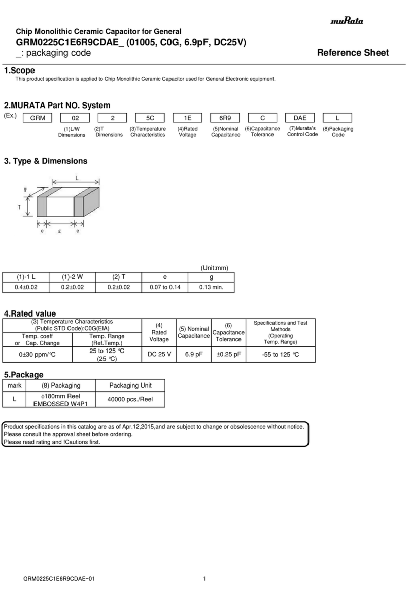
Murata GRM0225C1E8R2BDAE User manual

Murata
Murata GRM0225C1E6R9CDAE User manual

Murata
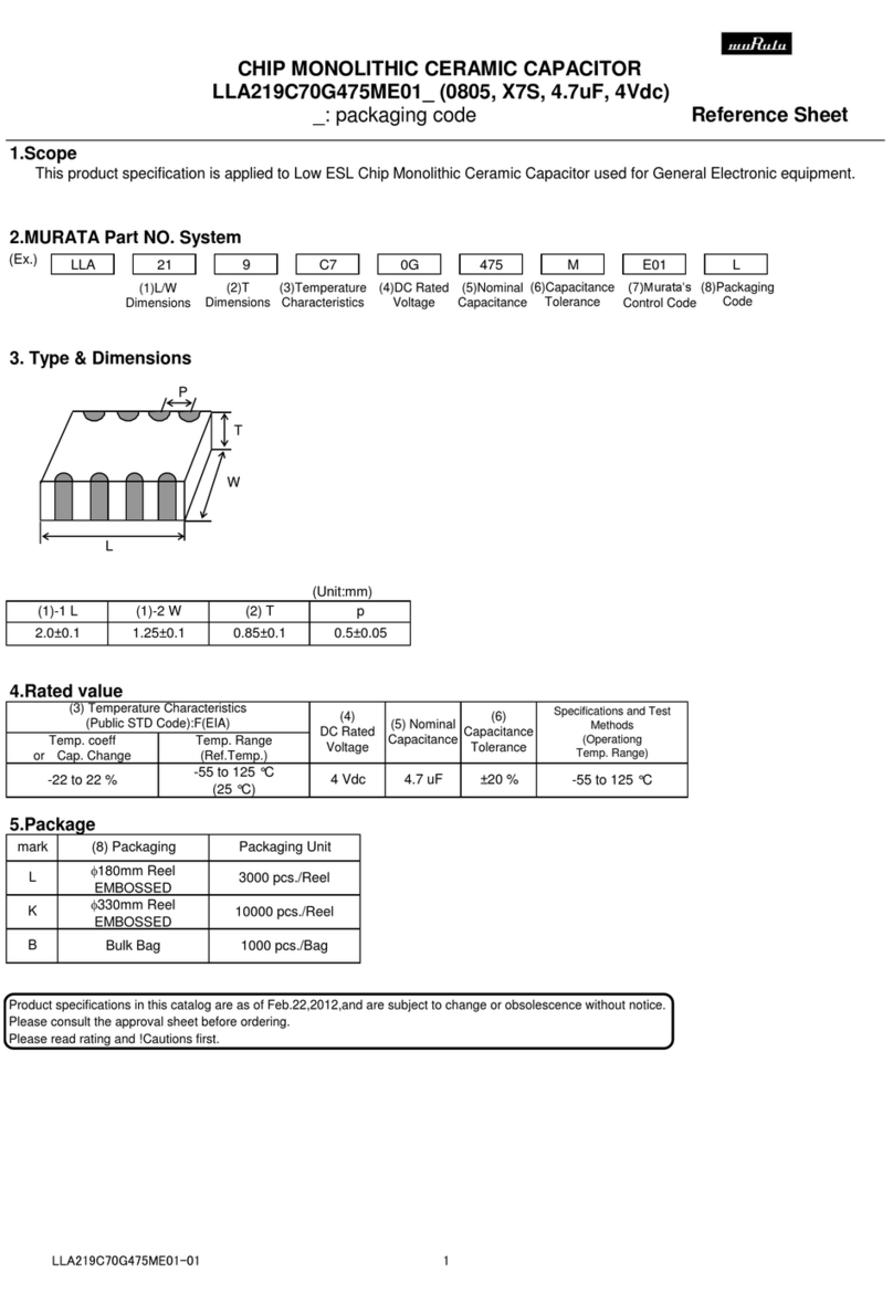
Murata LLA219C70G475ME01 Series User manual

Murata
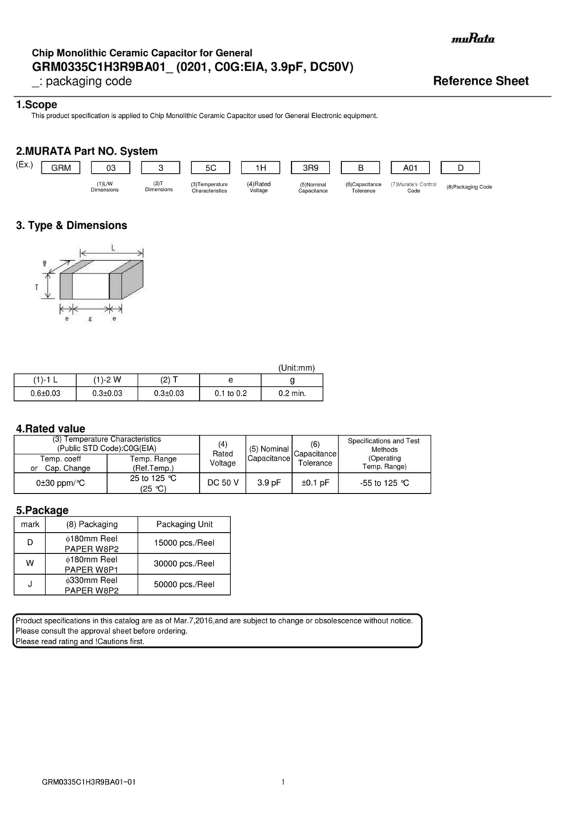
Murata GRM0335C1H3R9BA01 User manual

Murata
Murata GRM0225C1E8R4BDAE User manual

Murata
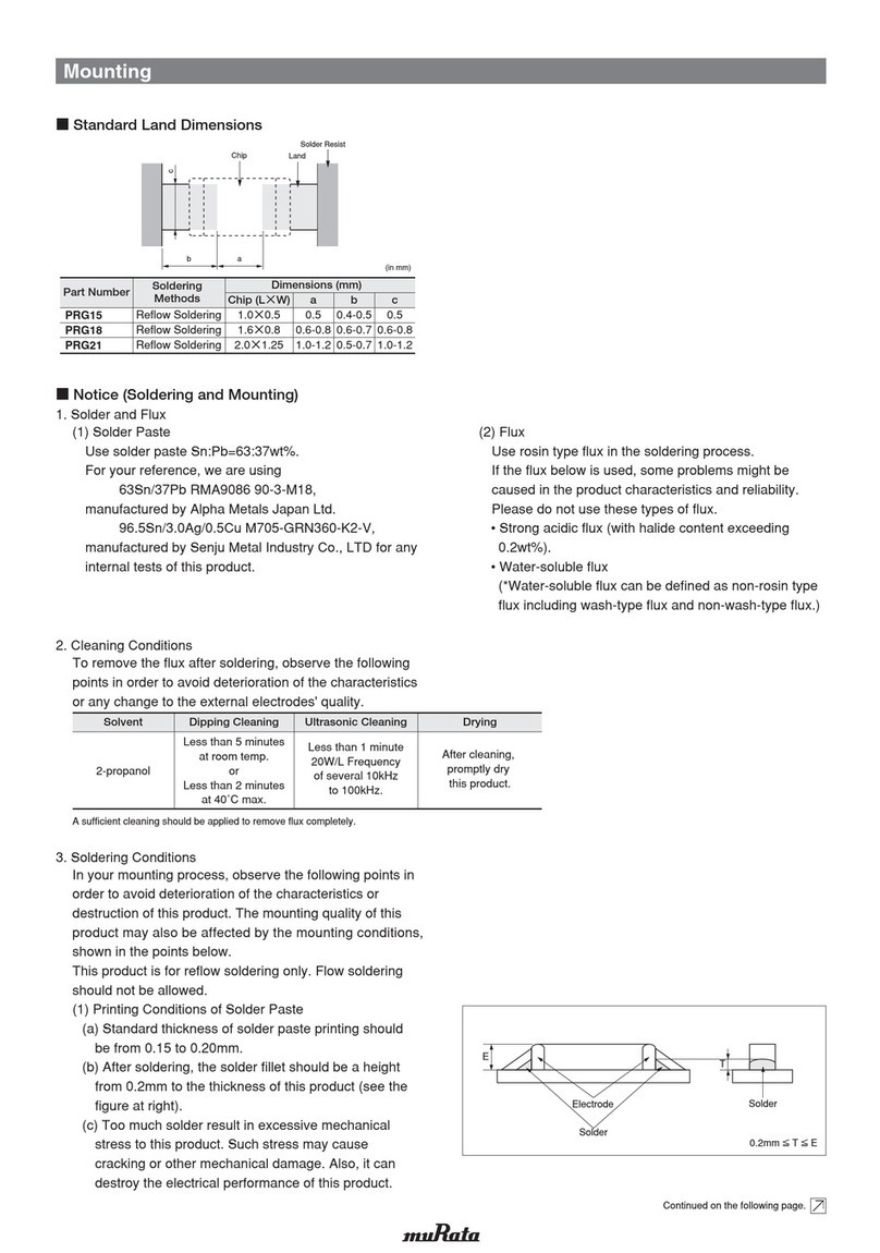
Murata PRG15 User manual

Murata
Murata SCC1000 Series User manual

Murata
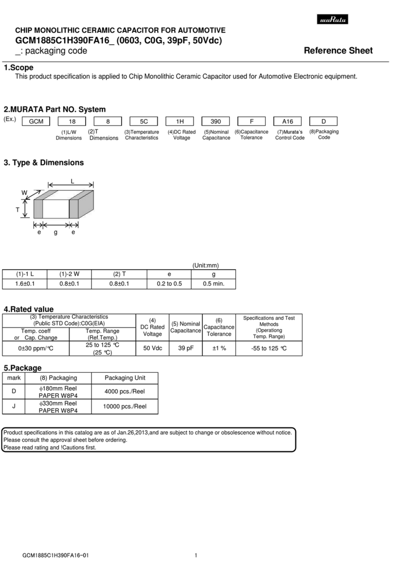
Murata GCM1885C1H390FA16D 0603 User manual
Popular Industrial Equipment manuals by other brands

GSI Group
GSI Group PNEG-1521 Assembly & operation manual

IKA
IKA RW 28 basic operating instructions

PHD
PHD GRA Series REPAIR PROCEDURES

Sealey
Sealey ADT200 quick start guide

Carl Valentin
Carl Valentin DYNACODE II Quick reference guide

Alemite
Alemite Carbon Shield CS-5700 Series Installation, operation and maintenance manual