Oki MSM7586-01 User manual

¡ Semiconductor MSM7586-01/03
1/42
¡ Semiconductor
MSM7586-01/03
p/4 Shift QPSK MODEM/ADPCM CODEC
GENERAL DESCRIPTION
The MSM7586 is a CMOS IC developed for use with digital cordless telephones. The device
provides a p/4 shift QPSK modem function and a CODEC function which performs transcoding
between the voice band analog signal and 32 kbps ADPCM data.
The MSM7586 performs DTMF tone and several types of tone generation, transmit/receive data,
mute and gain control, side-tone pass and its gain control, and VOX function.
FEATURES
(p/4 Shift QPSK Modem Unit)
• 384 kbps transmission speed
• Built-in root Nyquist digital filter for the baseband band limiter
• Built-in D/A converters for the analog outputs of the quadrature signal component I and Q
• The DC offset and gain can be adjusted with respect to the differential I and Q analog outputs
• Completely digitized p/4 shift QPSK demodulator system
(ADPCM CODEC Unit)
• ADPCM system: built-in ITU-T Recommendations G.726 (32kbps, 24 kbps, 16 kbps)
• Transmit/receive full-duplex capability
• PCM interface code format: selectable between m-law and A-law
• Serial ADPCM and PCM transmission rate: 64 kbps to 2,048 kbps
• Transmit/receive mute function; transmit/receive programmable gain setting
• Side tone generator (8-step level adjustment)
• Built-in DTMF tone, ringing tone, and various ringing tone generators
• Built-in VOX function
(Common Unit)
• Operate with a single 3 V power supply (VDD: 2.7 V to 3.6 V)
• Low power consumption
When entire system is operating: 20 mA Typ.
When powered down: 0.02 mA Typ.
• Package:
100-pin plastic TQFP (TQFP100-P-1414-0.50-K) (Product name: MSM7586-01TS-K)
(Product name: MSM7586-03TS-K)
E2U0034-28-82
This version: Aug. 1998
Previous version: Nov. 1996

¡ Semiconductor MSM7586-01/03
2/42
BLOCK DIAGRAM
Phase
detector
Delay
detector AFC
SL2
SL1
To each block
+1
–1
+1
–1
Root Nyquist LPF
PLL
3.84M
To D/A
S/P
MAPPING
1/10 384k
–
+
–
+
–1
–
+
4
<MODEM Unit>
<CODEC Unit>
TOUT3
PDN0
PDN1
PDN2
IFIN
IFCK
X2
X1
I+
I–
Q+
Q–
SGCR
AIN1–
AIN1+
GSX1
AIN2–
GSX2
AOUT+
AOUT–
PWI
VFRO
RXD
RXC
SLS
RPR
RCW
AFC
TXD
TXW
TXCI
TXCO
RSYNC
IR
PCMRO
PCMSO
BCLK
PCMSI
XSYNC
IS
VOXO
VDAM
AGM
VDDM
DGM
RXSC
MCK
MODEM
MCU
interface
EXCKM
DOUTM
DENM
DINM
R7, R6
R5, R4
To each block
BSTO
SGM
SGCT
IO2
IO1 SW1
SW2
VDAC
SAO
–
+
GSX3
AIN3
–
+
GSX4
AIN4
CODEC
MCU
interface
To each
block
VOXI
TOUT2
TOUT1
RESET
PDN3
AGC
DGC
VDAC
VDDC
IO7
IO6
SW5
IO5
SW4
IO4
IO3
SW3
EXCKC
DENC
DINC
DOUTC
VREF
DPLLDEC SL2
SL1
LPF
LPF
DC Adjust
DC Adjust
D/A
D/A
ATT
ATT
CRM1-B7 to B4
CRM1-B3 to B0
Receiver
Transmitter
CRC5-B7
CRC5-B6
R
R
T
CRC5-B5 CRC5-B4
VOICE
DETECT
COMPA
NDER
ADPCM
CODER
P
/
S
S
/
P
P
/
S
S
/
P
P
/
S
S
/
P
DTMF
/Tone
Generator
BPF
RC
Filter
A/D
Convertor
LPF
RC
Filter
D/A
Convertor
Noise
generator Power detect
+EXPAN
DER
ATT
ATT
CRC3-B7 to B5
CRC2-B2 to B0
CRC3-B3 to B0
Sign bit
ATT
CRC4-B6 CRC2-B6 to B4
PCMRI
ADPCM
DE-
CODER
CRC4-B5
T
R
T
CRM0-B6
Decision
To each
block
+
¡ Semiconductor MSM7586-01/03
3/42
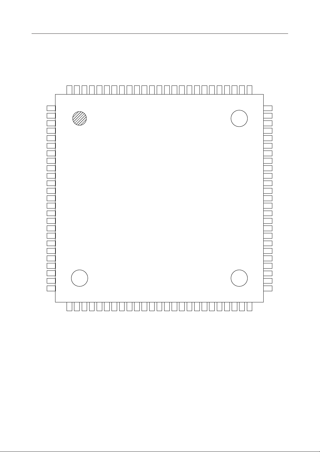
PIN CONFIGURATION (TOP VIEW)
100 VDDM
RXSC
SLS
IFIN
NC
X1
NC
NC
X2
IFCK
MCK
PDN0
PDN1
PDN2
NC
RCW
AFC
RPR
RXC
RXD
NC
DENM
EXCKM
DOUTM
DINM
SAO
AIN3
GSX3
VDAC
VDDC
NC
AIN4
GSX4
NC
IO3
IO4
NC
TOUT1
TOUT2
TOUT3
PDN3
RESET
NC
DINC
DOUTC
EXCKC
DENC
NC
VOXI
VOXO
VDAM
Q–
Q+
I–
I+
NC
SGM
AGM
AGC
SGCR
SGCT
AIN1+
AIN1–
GSX1
IO5
IO6
IO7
AIN2
GSX2
IO1
1
2
3
4
5
6
7
8
9
10
11
12
13
14
15
16
17
18
19
20
IO2
VFRO
PWI
AOUT–
AOUT+
21
22
23
24
25
NC
TXW
TXD
TXCO
TXCI
NC
BSTO
DGM
DGC
R7
R6
R5
R4
NC
BCLK
XSYNC
RSYNC
NC
PCMSO
PCMSI
75
74
73
72
71
70
69
68
67
66
65
64
63
62
61
60
59
58
57
56
IS
NC
IR
PCMRO
PCMRI
55
54
53
52
51
99
98
97
96
95
94
93
92
91
90
89
88
87
86
85
84
83
82
81
80
79
78
77
76
26
27
28
29
30
31
32
33
34
35
36
37
38
39
40
41
42
43
44
45
46
47
48
49
50
NC : No connect pin
100-Pin Plastic TQFP

¡ Semiconductor MSM7586-01/03
4/42
PIN AND FUNCTIONAL DESCRIPTIONS
(Modem Unit)
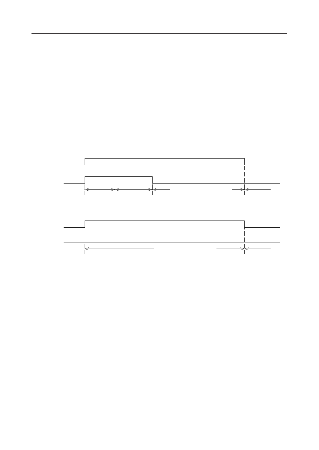
TXD
Transmit data input for 384 kbps.
TXCI
Transmit clock input.
When the control register CRM0 - B6 is "0", a 384 kHz clock pulse synchronous with TXD should
be input to this pin. This clock pulse should be continuous because this device use APLL to
generate an internal clock pulse.
When CRM0 - B6 is "1", a 3.84 MHz clock pulse should be input to this pin. When the 3.84 MHz
clock pulse is applied to TXCL, TXCO outputs a 384 kHz clock pulse, which is generated by
dividing the TXCL input by 10. The transmit data, synchronous to the 384 kHz clock pulse,
shouldbeinputtotheTXD.InthiscasethedevicesdonotuseAPLL,andthe3.84MHzclockpulse
need not be continuous. (Refer to Fig. 1.)
TXCO
Transmit clock output.
When CRM0 - B6 is "0", TXCO outputs the 384 kHz clock pulse (APLL output) for monitoring
purposes. When CRM0 - B6 is "1", this pin outputs a 384 kHz clock pulse generated by dividing
the TXCI input by 10. (Refer to Fig. 1.)
TXW
Transmit data window signal input.
The transmit timing signal for the burst data is input to this pin. If TXW is "1", the modulation
data is output. (Refer to Fig. 1)

¡ Semiconductor MSM7586-01/03
5/42
Figure 1 Transmit Timing Diagram
(1) CRM0 – B6 = "0"
Ramp rise-up
2 symbols
Ramp
Fall-down
2 symbols
(2) CRM0 – B6 = "1"
D0 D1 D2 D3 D4 D5 D6 D7 D8 D9 D10 D11 D12 D13 D
n
-1 D
n
,
D0 D1 D2 D3 D4 D5 D6 D7 D8 D9 D10 D11 D12 D13 D
n
-1 D
n
,
Ramp rise-up
2 symbols
Ramp
Fall-down
2 symbols
Delay of 6.25 symbols Delay of 6.25 symbols
Delay of 6.25 symbols Delay of 6.25 symbols
TXD
TXCI
(384 kHz)
TXW
TXCO
(384 kHz)
I, Q
TXD
TXCI
(3.84 MHz)
TXW
TXCO
(3.84 kHz)
I, Q

¡ Semiconductor MSM7586-01/03
6/42
BSTO
BSTO is the modulator side burst window output.
The burst position of the I and Q baseband modulator output is output.
I+, I–
Quadrature modulation signal I Component differential analog output.
Their output levels are 500 mVpp (when TXD = "0": 360 mVpp typ.) with 1.6 Vdc as the center
value. The output pin load conditions are: R ≥10 kW, C £ 20 pF. The gain of these pins can be
adjusted using the control register CRM1 - B7 to B4, and the offset voltage at the I– pin can be
adjusted using CRM3 - B7 to B3.
Q+, Q–
Quadrature modulation signal Q component differential analog outputs.
Their output levels are 500 mVpp (when TXD = "0": 360 mVpp typ.) with 1.6 Vdc as the center
value. The output pin load conditions are: R ≥10 kW, C £ 20 pF. The gain of these pins can be
adjusted using the control register CRM1 - B3 to B0, and the offset voltage at the Q– pin can be
adjusted by using CRM4 - B7 to B3.
SGM
Internal reference voltage output.
The output voltage value is approximately 2.0 V. Insert a bypass capacitor between this pin and
the AGM pin. During power down, this output is at 0 V.
The external SG voltage if necessary should be used via a buffer.

¡ Semiconductor MSM7586-01/03
7/42
PDN0, PDN1, PDN2
Various power down control.
PDN0 controls the standby mode/communication mode; PDN1 controls the modulator unit;
and PDN2 controls the demodulator unit. Refer to Table 1 for details.
The control register reset input width should be 200ns or more.
Modulator unit is powered off. (VREF and PLL are powered on.)
I and Q outputs are in a high impedance state.
Only the demodulator clock regenerator unit is powered on.
PDN0 PDN2 PDN1
Mode Name
Operation State
0 0/1 1 Mode A
1 0 0 Mode D
1 1 1 Mode G
Standby
Mode
Entire system is powered down. The control register is reset.
0 0 0 Mode BEntire system is powered down. The control register is not reset.
1 1 0 Mode FModulator unit is powered off. (VREF and PLL are powered off.)
I and Q outputs are in a high impedance state.
Demodulator unit is powered on.
1 0 1 Mode EModulator unit is powered on.
Only the demodulator clock regenerator unit is powered on.
Modulator unit is powered on.
Demodulator unit is powered on.
Commu-
nication
Mode
0 1 0 Mode CModulator unit is powered off. (VREF and PLL also powered off.)
Demodulator unit is powered on.
Table 1: Description of Modem Power Down Control

¡ Semiconductor MSM7586-01/03
8/42
VDDM, VDAM
+3 V power supply for the modem unit.
Supplied to the digital circuits through the VDDM pin and to the analog circuits through the
VDAM pin. VDDM and VDAM, and VDDC and VDAC should be connected as close as possible
on the PC board.
DGM, AGM
Ground pins for the modem unit.
DGM is the ground pin of the digital system, and AGM is the ground pin of the analog system.
Since DGM and AGM are isolated inside the IC, connect them as close as possible on the circuit
board.
MCK
Master clock input.
The clock frequency is 19.2 MHz.
IFIN
Modulated signal input for the demodulator block.
Select the IF frequency can be selected from 1.2 MHz, 10.7 MHz, 10.75 MHz, and 10.8 MHz, based
on CRM0 - B4 and B3.
IFCK
Clock frequency 19.0222 MHz input for demodulator block IF frequencies of 10.7 MHz.
If the IF frequency is 1.2 MHz or 10.8 MHz, set this pin to "0" or "1". (Refer to Fig. 2.)
X1, X2
Crystal oscillator connection pins.
When supplying a 19.0222 MHz clock to IFCK, use these pins. (Refer to Fig. 2.)
Figure 2 How to Use IFCK, X1, and X2
When IFIN = 10.7 MHz
MSM7586
X1 X2 IFCK
19.0222 MHz
When IFIN = 1.2 MHz or 10.8 MHz
MSM7586
X1 X2 IFCK

¡ Semiconductor MSM7586-01/03
9/42
RXD, RXC, RXSC
Receive data and receive clock outputs.
When the modem unit is powered on, RXD, RXC and RXSC are selected based on SLS as shown
in Figure 3. These outputs are used by the clock regenerator circuit.
Figure 3 Timing Diagram of RXD, RXC, and RXSC
SLS
Receive side operation slot selection signal.
This device has two clock regenerator circuits and two AFC data memory registers. If SLS is "0",
slot 1 is selected, if SLS is "1", slot 2 is selected.
RPR
High-speed phase clock control signal input for the clock recovery circuit.
If this pin is at "0", the circuit is always in the low-speed phase clock mode. If this pin is at "1",
the clock recovery circuit enters the high-speed phase clock mode. When the phase difference
is less than a defined value, the circuit shifts to the low-speed phase clock mode automatically.
RXD
RXC
RXSC
SLS 1 Symbol The regenerated data and clock are
selected asynchronously by the SLS signal.
¡ Semiconductor MSM7586-01/03
10/42
AFC
AFC operation range specification signal input.
As shown in Fig. 4, the AFC information is reset when both AFC and RPR are set to "1". AFC
operation starts after a fixed number of clock cycles and the AFC information is reset. If RPR is
set to "1", an average number of times that AFC turns on is low. If RPR is "0", AFC is high. If AFC
is "0", frequency error is not calculated, but the frequency is corrected using an error that is held.
RCW
Clock recovery circuit operation ON/OFF control signal input.
If RCW this pin is "0", DPLL does not make any phase corrections.
AFC
AFC information
is reset.
RPR
Average
number of times
AFC is low.
AFC information
is maintained.
AFC
RPR
AFC information
is maintained.
The clock recovery circuit
starts with the previous
AFC information.
"0"
(CASE1)
(CASE2)
Average number of times
AFC is high.
Average number of times
AFC is high.
Figure 4 AFC Control Timing Diagram
DENM , EXCKM, DINM, DOUTM
Serial control ports for the microprocessor interface.
The device contains a 6-byte control register (CRM0 - 5). An external CPU uses these pins to read
data from and write data to the control register. DENM is the "Enable" signal input pin. EXCKM
is a data shift clock pulse input pin. DINM is an address and data input pin. DOUTM is a data
output pin. Figure 5 shows input/output timing diagram.
This manual suits for next models
1
Table of contents


