TPC8402
2006-11-13
1
TOSHIBA Field Effect Transistor Silicon N, P Channel MOS Type (π−MOSVI/U−MOSII)
TPC8402
Lithium-Ion Secondary Battery Applications
Notebook PCs
Portable Equipment Applications
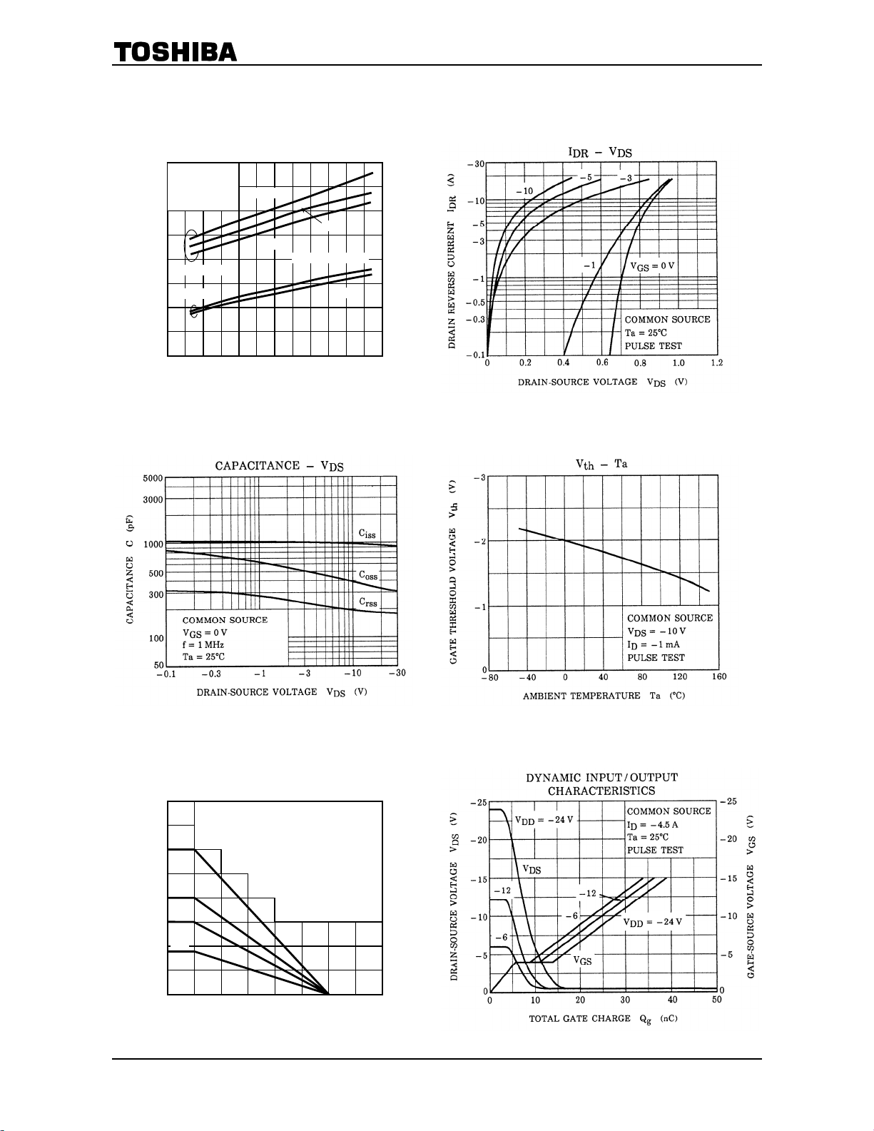
zLow drain−source ON resistance : P Channel RDS (ON) = 27 mΩ(typ.)
N Channel RDS (ON) = 37 mΩ(typ.)
zHigh forward transfer admittance : P Channel |Yfs| = 7 S (typ.)
N Channel |Yfs| = 6 S (typ.)
zLow leakage current : P Channel IDSS = −10 µA (VDS = −30 V)
N Channel IDSS = 10 µA (VDS = 30 V)
zEnhancement−mode
: P Channel Vth = −0.8~ −2.0 V (VDS = −10 V, ID= −1mA)
N Channel Vth = 0.8~2.0 V (VDS = 10 V, ID= 1mA)
Absolute Maximum Ratings (Ta = 25°C)
Rating
Characteristics Symbol P Channel N Channel Unit
Drain-source voltage VDSS −30 30 V
Drain-gate voltage (RGS =20 kΩ) VDGR −30 30 V
Gate-source voltage VGSS ±20 ±20 V
DC (Note 1) ID−4.5 5
Drain current
Pulse (Note 1) IDP −18 20
A
Single-device operation
(Note 3a)
PD (1) 1.5 1.5
Drain power
dissipation
(t = 10s)
(Note 2a)
Single-device value at
dual operation (Note 3b) PD (2) 1.0 1.0
Single-device operation
(Note 3a)
PD (1) 0.75 0.75
Drain power
dissipation
(t = 10s)
(Note 2b)
Single-device value at
dual operation (Note 3b) PD (2) 0.45 0.45
W
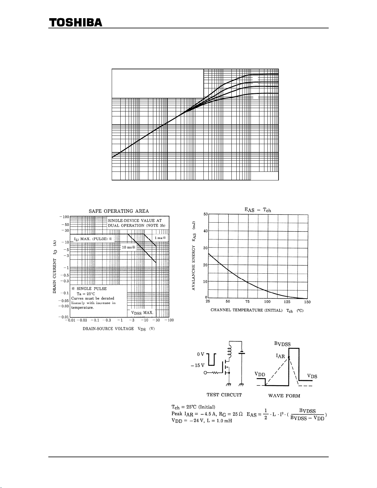
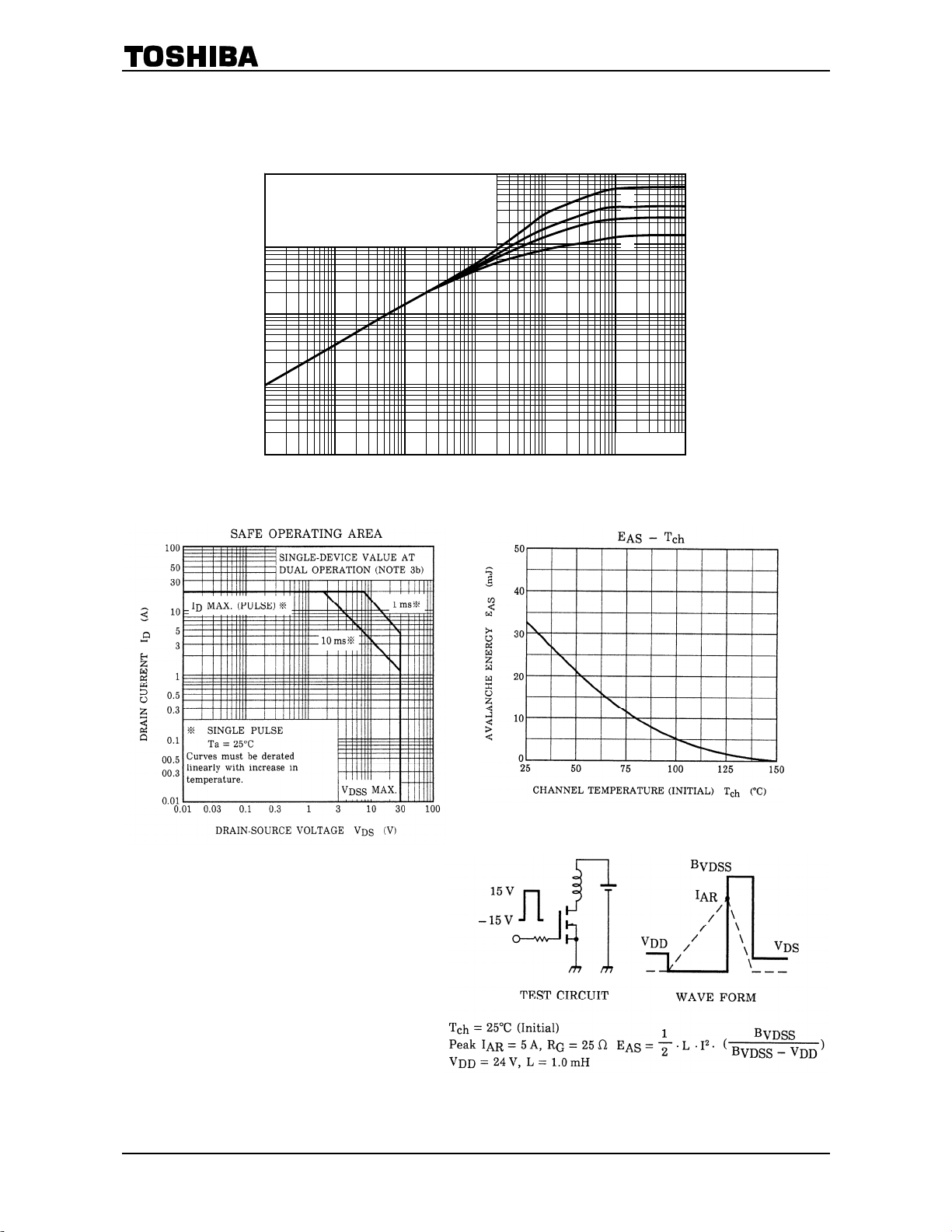
Single-pulse avalanche energy EAS 26.3
(Note 4a)
32.5
(Note 4b) mJ
Avalanche current IAR −4.5 5 A
Repetitive avalanche energy
Single-device value at operation
(Note 2a, Note 3b, Note 5)
EAR 0.10 mJ
Channel temperature Tch 150 °C
Storage temperature range Tstg −55~150 °C
Note: For Notes 1 to 5, see the next page.
Using continuously under heavy loads (e.g. the application of high temperature/current/voltage and the
significant change in temperature, etc.) may cause this product to decrease in the reliability significantly even
if the operating conditions (i.e. operating temperature/current/voltage, etc.) are within the absolute maximum
ratings.
Please design the appropriate reliability upon reviewing the Toshiba Semiconductor Reliability Handbook
(“Handling Precautions”/Derating Concept and Methods) and individual reliability data (i.e. reliability test report
and estimated failure rate, etc).
This transistor is an electrostatic-sensitive device. Handle with care.
Unit: mm
JEDEC ―
JEITA ―
TOSHIBA 2-6J1E
Weight: 0.080 g (typ.)
Circuit Configuration