ORTEC 451 User manual

INSTRUCTION MANUAL
451
SPECTROSCOPY AMPLIFIER
Serial No.
Purchaser
Date Issued
100 MIOLANO ROAD
OAK RIDGE. TENN. 37830
PHONE I6151 482-4411
TWX 810-572-1078

TABLE OF CONTENTS
Page
WARRANTY
PHOTOGRAPH
1. DESCRIPTION
1.1 General Description
1.2 PolsZero Cancellation
1.3 Active Filter
l-l
I-1
l-2
1-2
2. SPECIFICATIONS
2.1 Electrical
2-1
2-1
3. INSTALLATION 3-1
3.1 General Installation Considerations
3.2 Connection to Preamplifier
3.3 Connection of Test Pulse Generator
3.4 Connection to Power - Nuclear Standard Bin, ORTEC 401A/402A
3.5 Shaping Considerations
3.6 Use of Delayed Output
3.1 Output Connections and Tern+nating Considerations
3.8 Shorting 01 Overloading the Amplifier Outputs
4. OPERATING INSTRUCTIONS
3.1
3-1
3-1
3-2
3-2
3-2
3-2
3-3
4-l
4.1 Front Panel Controls 4-1
4.2 Rear Panel Controls 4.1
4.3 Internal Contmlr 4-1
4.4 Fmnt Panel Connectors (All Type BNCI 4.1
4.5 Rear Panel Connectors 4-3
4.6 Initial Testing and Observation of Pulse Waveforms 4-3
4.7 General Considerations for Operation with Semiconductor Detectors 4-3
4.8 Operation in Spectroscopy Systems 4.10
4.8 Typical System Block Diagrams (Figurer 4-12 through 415) 4.11
4.10 Baseline Restorer (BLR) 4-11
4.11 Methods of Connection to Various Analyzers 4.18
6. CIRCUIT DESCRIPTION 5-1
6. MAINTENANCE 6-1
8.1 Test Equipment Required 6-1
8.2 Pulser Modifications for Overload Tests 6-1
6.3 Pulser Testr 6-1
6.4 Suggestions for Troubleshooting 6-3
8.5 Tabulated Test Point Voltages on Etched Board 8-4

LISTOF FIGURESAND ILLUSTRATIONS
Figure l-1 Clipping in a Non-PoleZero Can&led Amplifier 1-3
Figure l-2 Differentiation (Clipping) in a PoleZero Cancelled Amplifier 1-3
Figure 1-3 Pulse Shapes for Good Signal-to-Noise Ratios 1-4
Figure 4-l Effects of Shaping Time Selection on Output Waveforms 4-2
Figure 42 Measuring Amplifier end Detector Noise Resolution 4-4
Figure 4-3 Resolution Effects of Capacitance 4-6
Figure 4-4 Noise as a Function of Bias Voltage 4-6
Figure 4.5 System For Measuring Resolution With a Pulse Height Analyzer 4-7
Figure 46 System For Detector Current and Voltage Measurements 4-8
Figure 47 Silicon Detector Back Current Versus Bias Voltage 4-8
Figure 4-8 System For High Resolution Alpha Particle Spectmscopy 4-9
Figure 49 System For High Resolution Gamma Spectroscopy 4-9
Figure 410 Scintillation Counter Gamma Spectroscopy System 4.12
Figure411 High Resolution X-Ray Spectroscopy System 4.12
Figure 4-12 Gamma-Gamma Coincidema Experiment-Block Diagram 4-13
Figure 413 Gamma Ray-Charged Particle Coincidence Experiment-Block Diagrams 4-14
Figure 4-14 Gamma Ray Pair Spectrometer-Block Diagrams 4.14
Figure4.15 General System Arrangement for Gating Control 4.15
Figure 4-16 Analyzer Connection With No Trigger Required 4-16
Figure 417 Analyzer Connection When Trigger is Required 4.16
Figure 418 Effects of Baseline Restorer on Resolution 4.17

A NEW STANDARD TWO-YEAR WARRANTY FOR ORTEC ELECTRONIC INSTRUMENTS
ORTEC warrants its nuclear instrument products to be free from defects in workmanship and materials, other
than vacuum tubss and semiconductors, for a period of twenty-four months from date of shipment, provided
that the equipment has been used in a proper manner and not subjected to abuse. Repairs or replacement, et
ORTEC optil~ n, will be made without charge at the ORTEC factory. Shipping expense will be to the account
of the customer except in cases of defects discovered upon initial operation. Warranties of vacuum tubes and
semiconductors, as made by their manufacturers, will be extended to our customers only to the extent of the
manufacturers’ liability to OATEC. Specially selected vacuum tubes or semiconductors cannot be warranted.
ORTEC reservestheright to modify the design of its products without incurring responsibility for modification
of previously manufactured units. Since installation conditions are beyond our control. ORTEC does not
assume any risks or liabilities associated with methods of installation other than specified in the instructions,
or imtallation results.
OUALITY CONTROL
Before being approved for shipment, each ORTEC instrument must pass a stringent set of quality control tests
designed to expose any flaws in materials or workmanship. Pwmanent records of these tests are maintained for
use in warranty repair and as a source of statistical information for design improvements.
REPAIR SERVICE
ORTEC instruments not in warranty may be returned to the factory for repairs or checkout at modest expense
to the customer. Standard procedure requires that returned instruments pass the same quality control tets as
those used for new production instruments. Please contact the factory for instructions before shipping
equipment.
DAMAGE IN TRANSIT
Shipments should be examined immediately upon receipt for evidence of external or concealed damage. The
carrier making delivery should be notified immediately of any such damage, since the carrier is normally liable
for damage in shipment. Packing materials, waybills, and other such documentation should be preserved in
order to establish claims. After such notification to the carrier, please notify ORTEC of the circumstances so
that we may assist in damage claims and in providing replacement equipment if necessary.


!)?I u !L3 ll
IIE!;TOIIE
IEUY HI

ORTEC 451
SPECTROSCOPY AMPLIFIER
1-1
1. DESCRIPTION
1.1 General Description
The ORTEC 451 Spectroscopy Amplifier is a single width NIM module with a versatile combination
of switch selectable pulse shaping and output characteristics. It features extremely low noise, wide gain
range, and excellent overload response for universal application in high resolution spectroscopy. It
accepts input pulses of either polarity which originate in germanium or silicon semiconductor detectors.
scintillation detectors with either fast or slow scintillaton, proportional counters. pulsed ionization
chambers, electron multiplixs, etc.
The 451 has a dc input impedance for approximately 1000 ohms and accepts either positive or negative
input pulses with rise times < 650 nsec and fall times > 25!~sec. Three integrate and differentiate time
constants are separately switch selectable to provide optimum shape for resolution and count rate. The
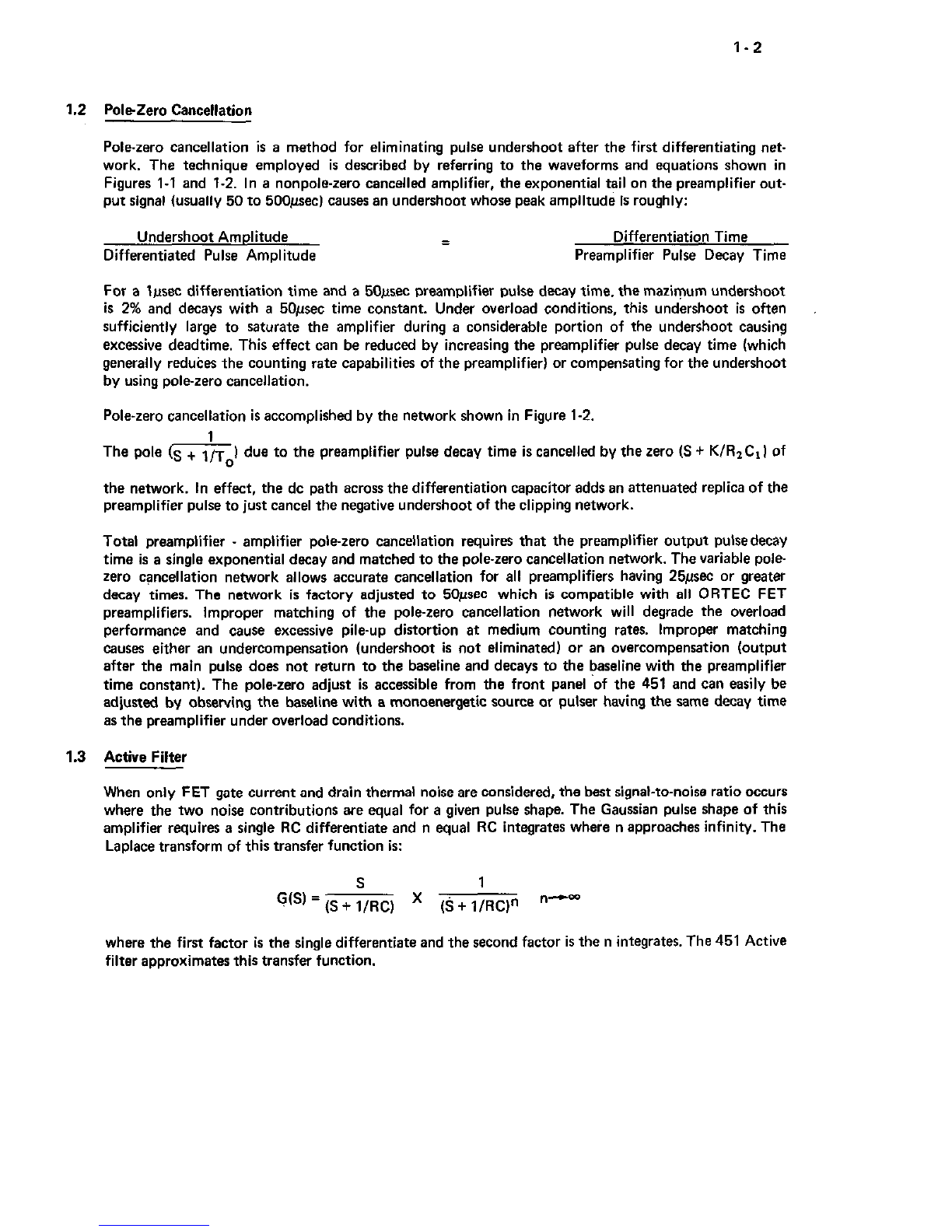
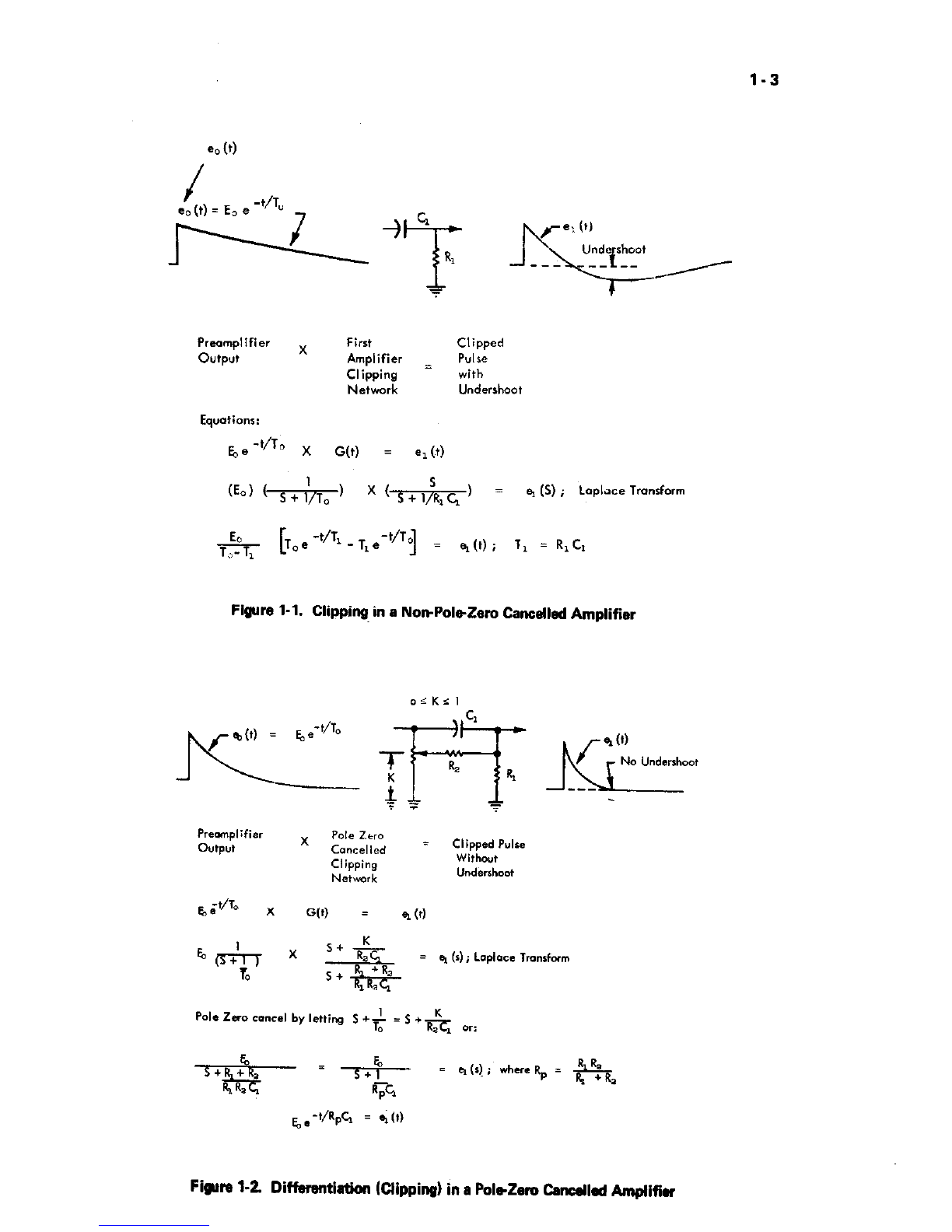
first differentiation network has variable pole-zero cancellation which can be adjusted to match
preamplifiers with > 25psec decay time. The pole-zero cancellation drastically reduces the undershoot
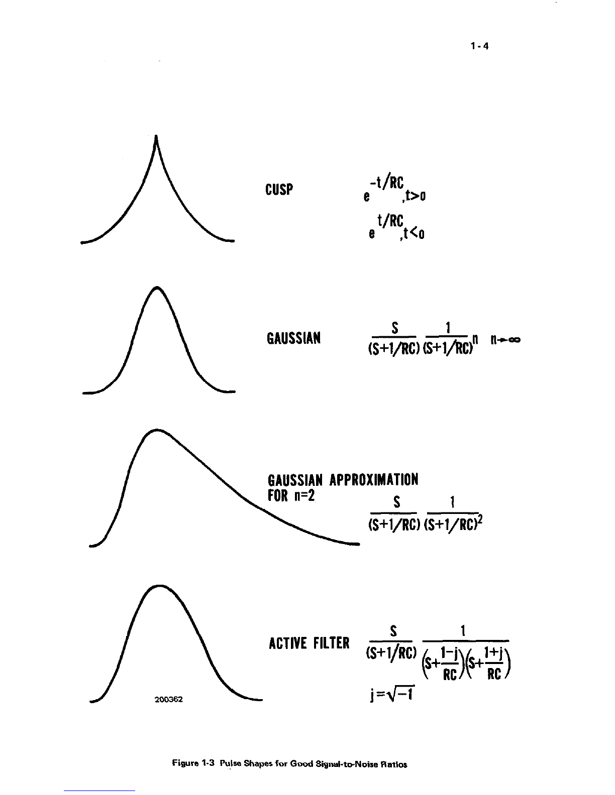
after the first clip and greatly improves overload characteristics. In addition, the amplifier contains an
active filter shaping network which optimizes the signal to noise ratio and minimizes the overall
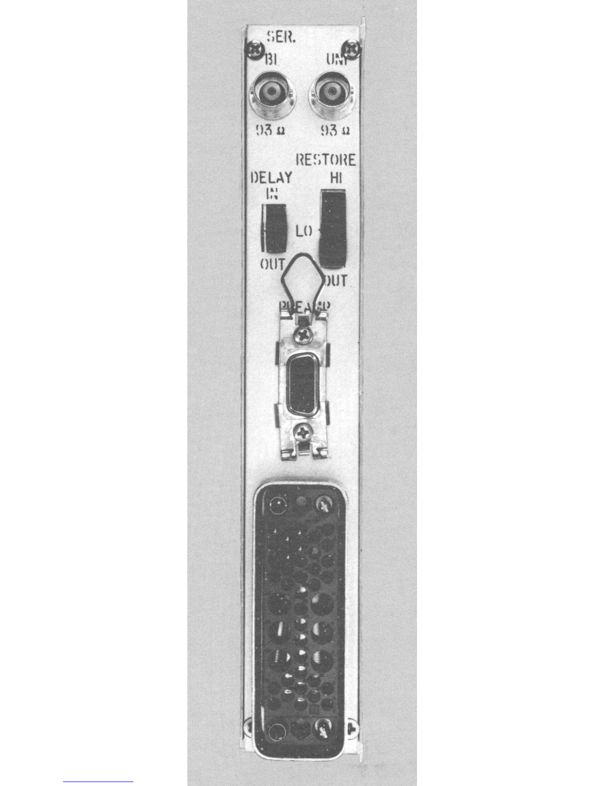
resolving time. Both unipolar and bipolar outputs are provided simultaneously on the front and rear
panels.
The unipolar output should be used for spectroscopy when dc coupling can be maintained from the 451
Amplifier to the analyzer. A BLR (Base Line Restoration) circuit is included in the 451 for improved
performance at high count rates. A switch on the rear panel permits this circuit to be switched out. set
for low count rates, or set for high count rates. When using the direct coupled input of the various
analyzers, a variety of voltage requirements exist. To meet these requirements the 451 unipolar out!
put can be selected for either positive or negative polarity and selected for full scale voltage of 3V,
6V. or 1OV. The unipolar output dc level can be adjusted from -IV to +lV. This output permits the
use of the direct coupled input of analyzers with a minimum amount of interface problems. The 451
bipolar output may be preferable for spectroscopy when operating into an x-coupled system at high
counting rates.
The 451 can be used for crossover timing when used in conjunction with an ORTEC 407 Crossover Pick-
off or a 420A Timing Single Channel Analyzer. The 420A Timing Single Channel Analyzer output has a
minimum of walk as a function of pulse amplitude and incorporates a variable delay time on the output
pulse to enable the crosswer pickoff output to be placed in time coincidence with other outputs. A
switch selectable 2psec delay is provided on the unipolar output to aid in obtaining the proper spacing
of the linear pulse in a coincidence gated system.
The 451 has complete provisions including power for operating any ORTEC solid state preamplifier
such as the 109A. 113, 118A. and 120. Preamplifier pulses should have a rise time of 0.5jJsec or less, to
properly match the amplifier filter network and a decay time > 25!.1sec for proper pole-zero cancella-
tion. The 451 input impedance is 1000 ohms. When long preamplifier cables are used, the cables can be
terminated in series at the preamplifier end or in shunt at the amplifier end with the proper resistors.
The output impedance of the 451 is about 0.1 ohm at the front panel connectors and 93 ohms at the
rear panel connectors. The front panel outputs can be connected to other equipment by single cable
going to all equipment and shunt terminated at the far end. If series termination is desired, the rear
panel connectors can be used in connecting the 451 to other modules (see Section 3).
Gain changing is accomplished by varying feedback networks. These networks are varied in such a
manner that the band width of the fedback amplifier stages remain essentially constant regardless to
gain and, therefore, rise time changes with gain switching (which cause crossover walk) are limited to
small variations.

1-2
1.2 PoleZero Cancellation
Pole-zero cancellation is a method for eliminating pulse undershoot after the first differentiating “et-
work. The technique employed is dexribed by referring to the waveforms and equations show” in
Figures l-l and 1-2. In a nonpole-zero cancelled amplifier, the exponential tail on the preamplifier out-
put signal (usually 50 to 500&1sec) causes a” undershoot whose peak amplitude is roughly:
Undershoot Amplitude Differentiation Time
Differentiated Pulse Amplitude Preamplifier Pulse Decay Time
For a lpsec differentiation time and a 5Opsec preamplifier pulse decay time. the mazimum undershoot
is 2% and decays with a 50!.1sec time constant. Under overload conditions, this undershoot is often
sufficiently large to saturate the amplifier during a considerable portion of the undershoot causing
excessive deadtime. This effect can be reduced by increasing the preamplifier pulse decay time (which
generally redu&s the counting rate capabilities of the preamplifier) or compensating for the undershoot
by using pole-zero cancellation.
Pole-zero cancellation is accomplished by the network shown in Figure 1-2.
The pole ho) due to the preamplifier pulse decay time is cancelled by the zero (S + K&C, I of
the network. In effect, the dc path across the differentiation capacitor adds a” attenuated replica of the
preamplifier pulse to just cancel the negative undershoot of the clipping network.
Total preamplifier - amplifier pole-zero cancellation requires that the preamplifier output pulsedecay
time is a single exponential decay and matched to the pole-zero cancellation network. The variable pole-
ZWCI c~ncellatio” network allows accurate cancellation for all preamplifiers having 25~~ or greater
decay times. The network is factory adjusted to 50~s~ which is compatible with all ORTEC FET
preamplifiers. Improper matching of the pole-zero cancellation network will degrade the overload
performance and cause excaive pile-up distortion at medium counting rates. Improper matching
causes either a” undercompensation (undershoot is not eliminated) or a” overcompensation (output
after the main pulse does not return to the baseline and decays to the baseline with the preamplifier
time constant). The pole-zero adjust is accessible from the front panel of the 451 and can easily be
adjusted by observing the baseline with a monoenergetic source or pulser having the same decay time
as the preamplifier under overload conditions.
1.3 Active Filter
When only FET gate current and drain thermal noise are considered, the best signal-to-noise ratio occurs
where the two noise contributions are equal for a give” pulse shape. The Gaussian pulse shape of this
amplifier requires a single RC differentiate and n equal RC integrates where n approaches infinity. The
Laplace transform of this transfer function is:
S 1
G’S) = (S + l/RC) x (S + l/RC)” “---
where the first factor is the single differentiate and the second factor is the n integrates. The 451 Active
filter approximates this transfer function.

1-3
F
Prsamplifier X Fir*, Clipped
0”tp”t Amplifier P”lW
Clipping = with
Netwok Undershoot
Equationr:
E?e -t/To X G(t) = e, 0)
(Ea) (+) X ( s + ,,& ) = e, (5) i W=e Tmnsfmm
&. [T,e-t’T1-Tl.-“T,l = e,(t); 1, = R,C,
Figure l-l. Clipping in a Non-PoleZem Cancellad Amplifier
TT&- = s+R;G = h(l); whRp’ **
Fiwm l-2. Diffemntiation (clipping) in a P&Zen, Cancrlld Amptifin

1-4
CUSP -t/lx
e ,t>0
t/RC
e ,t<ll
GAUSSIAN s 1
(s+l/Rc) 6+1/k” “--==
ACTIVEFILTER (S+& ($-i;++~)
j=fi
Figure 1-3 P+a Shapes for Good Sinai-tddoira Ratios

2-l
2. SPECIFICATIONS
2.1 Electrical
INPUT
OUTPUTS
UNIPOLAR
BIPOLAR
PERFORMANCE
Gain Range
Integral Non-linearity
Noise
Temperature Stability
Gain
DC Level
Crossover Walk
countRate
Stability
Overload
Recovery
CONTROLS
FINE GAIN
Positive or negative output from a preamplifier; rise
time 10 to 650 nsec; decay time 25 to 2000 pssec; Zin
2 lOOOn dc-coupled; max linear input 5.5 volts; max
input 20V; switch selectable active baseline restorer rate
Prompt or delayed with full scale linear range of f3,
f6, or flOV as selected; *12V max; active filter shaped;
dc restored, with switch selectable active baseline.
restorer rate, and baseline level adjustable to *l.OV; Z,
<I.Q front panel, and 93& rear panel, short circuit
proof .
Prompt output with positive lobe leading, with linear
range 0 to flOV independent of Unipolar range and
polarity; f12V max; active filter shaped; Z, <la,
front panel, and 930., rear panel, short circuit proof
With a nine-position Coarse selection from x5 tox2000,
and ten-turn potentiometer for Fine adjustment from
x0.5 to x1.5, total gain is the product of Coarse and
Fine Gain settings; Coarse Gain factors obtained by
feedback techniques
Internal switches permit independent selection of inte-
gration and differentiation time constants I? = 0.5, 1,
cu 2 ptsec); time to Unipolar peak = 27; time to Bipolar
crossover = 2.6~
<0.05%
<E+V (Unipolar), or <BpV (Bipolar). referred to the
input, with 2 !xec shaping and Coarse Gain alO0
o.oo5%Pc, 0 to 50x
<05mV/~C, 0 to 5oqc
e4 nsec for 2O:l dynamic range, including contri-
bution of ORTEC 420A Timing Single Channel Analyzer
A pulser peak at 85% of analyzer range shifts less than
0.2% in the presence of 0 to 5 x 10⁴ random cps from a
“‘Cs source with its peak stored at 75% of analyzer
range, using 1 psec filter time constants
Recovers to within 2% of rated output from 1000X
overload in 2.5 non-overloaded Bipolar pulse widths,
using maximum gain; degrades to 200X for Unipolar
pulse shaping
Ten-turn precision potentiometer for continuously vari-
able direct reading gain factor of x0.6 to x1.5

2-2
COARSE GAIN
INPUT POLARITY
UNIPOLAR OUTPUT
PZ ADJ
DC ADJ
DELAY
BLR
SHAPING
OUTPUT RANGE
CONNECTORS
INPUT
UNIPOLAR
OUTPUT
BIPOLAR
OUTPUT
PREAMP
POWER AND MECHANICAL
Power Required
Shipping Weight *
Net Weight
Nine-position switch, selects feedback resistors for gain
factors of x5, 10, 20, 50, 100, 200, 500, 1K. and 2K.
Slide switch, sets input circuit for either POS or NEG
input polarity
Slide switch, selects either POS or NEG Unipolar output
Potentiometer to adjust Pole-Zero cancellation for decay
times from 25 wet to m
Potentiometer to adjust the DC level for Unipolar out-
p”ts; range f1.5V
Slide switch, selects either 2 @ec delay (INI or prompt
(OUT) output for the Unipolar signals
Three-position slide switch, selects baseline restorer
function; HI for duty cycles >15%, LO for duty cycles
<15%, or OUT
Five three-position slide switches (Sl to S5) on side
panel, each identified for its filtering function; selects
time constants of 0.5, 1, or 2 ~.lsec independently
Three-position slide switch on side panel, selects full
range for Unipolar outputs at 3, 6, or 1OV (the Bipolar
output range is always 0 to IOV, independent of the
selected Unipolar output range)
BNC (UG-1094/U), front panel
BNC (UG-1094/U), front panel for 2, <la, rear panel
for 2, = 93.0
BNC (UG-1094/U). front panel for 2, <la, rear panel
for 2, = 93a
Standard ORTEC power connector for mating pream-
plifier; Amphenol type 17-10090; rear panel
t24V 85mA +12v 15mA
-24V 85mA -12v 15mA
7 pounds (3 kg)
3.3 pounds (1.5 kg)
Standard single width module (1.35 by 8.714 inches)
per TID-20893 (Rev.1

3-1
3. INSTALLATION
3.1 General Installation Coniiderations
The 451, used in conjunction with a 401Al402A Bin and Power Supply is intended for rack mounting;
therefore, it is necessary to ensure that vacuum tube equipment operating in the same rack with the
451 has sufficient cooling air circulating to prevent any local&d heating of the all-semiconductor
circuitry used throughout the 451. The temperature of equipment mounted in racks can easily exceed
120°F (50°C) unless precautions are taken.
3.2 Connection to Preamplifier
The preamplifier output signal is connected to the 451 via BNC connector CN5 labeled INPUT. The
input impedance is 1000 ohms and is decoupled to ground; therefore, the output of the preamplifier
must be either x-coupled or have approximately zero dc voltage under no signal conditions.
The 451 incorporates pole-zero cancellation in order to enhance the overload characteristics of the
amplifier. This technique requires matching the network to the preamplifier decay time constant in
order to achieve perfect compensation. The network is variable and factory adjusted to 5Ofisec to
match all ORTEC FET preamplifiers. If other preamplifiers or more careful matching is desired, the
adjustment is accessible from the front panel. Adjustment is easily accomplished by using a mono-
energetic source and observing the amplifier baseline after each pulse under overload conditions.
Preamplifier power of +24V. +lZV, -12V. and -24V is available on the preamp power connector, CN6.
When using the 451 with a remotely located preamplifier (i.e.. preamplifier-to-amplifier connection
through 25 feet or more of coaxial cable), care must be taken to ensure that the characteristic imped-
ance of the transmission line from the preamplifier output to the 451 input is matched. Since the
input impedance of the 451 is 1000 ohms, sending end termination will normally be preferred; i.e.. the
transmission line should be series terminated at the output of the preamplifier. All ORTEC preamplifiers
contain Series terminations which are either 93 ohms or variable: coaxial cable type RG-62/U or
RG-71/U is recommended.
3.3 Connection of Test Pulse Generator
3.3.1 Connection of Pulse Generator to the 451 Through a Preamplifier
The satisfactory connection of a test pulse generator such as the ORTEC 419 or equivalent
depends primarily on two considerations: (1) the preamplifier must be properly connected to the
451 as dixussed in Section 3.2, and (2) the proper input signal simulation must be applied to the
preamplifier. To ensure proper input signal simulation, refer to the instruction manual for the
particular preamplifier being used.
3.3.2 Direct Connection of Pulse Generator to the 451
Since the input of the 451 has 1000 ohms input impedance, the test pulse generator will normally
have to be terminated at the amplifier input with a” additional shunt resistor. I” addition, if the
test pulse generator has a dc offset greater than 1V. a large series isolating capacitor is also
required since the inputs of the 451 are dc-coupled. The ORTEC 204 or 419 Test Pulse Generators
are designed for direct connection. When either of these units is used, they should be terminated
with a 100 ohm terminator at the amplifier input or used with at least one of the output attenua-
tors set at IN. (The small error due to the finite input impedance of the amplifier can normally be
neglected.)
3.3.3 Special Test Pulse Generator Considerations for Pole-Zero Cancellation
The pole-zero cancellation network in the 451 is factory adjusted for a 50~s~ decay time to
match ORTEC FET preamplifiers. When a tail pulser lsuch as the 204 or 419) is connected

3-2
directly to the amplifier input, the pulser should be modified to obtain a 5O/l.%?c decay time or
the P-Z ADJ should be adjusted if overload tests are to be made (other tests are not affected). Sea
Section 6.2 for the details on this modification.
If a preamplifier is used and a tail pulser connected to the preamplifier test pulse input. similar
precautions are necessary. In this case, the effect of the pulser decay must be removed, i.e., a
step input should be simulated. Details for this modification are also given in Section 6.2.
3.4 Comae&on to Power - Nuclear Standard Bin, ORTEC 401A/402A
The 435A contains no internal power supply and therefore must obtain power from a Nuclear Standard
Bin and Power Supply such as the 401A/402A. It is recommended that the bin power supply be turned
off when inserting or removing modules. The ORTEC 400 Series is designed so that it is not possible to
overload the bin power supply with a full complement of modules in the Bin; however, this may not be
true when the Bin contains modules other than those of ORTEC design, and in this case, the power
supply voltages should be checked after insertion of the modules. The 401A/402A has test points on
the power supply control panel to monitor the dc voltages.
3.5 Shaping Con&rations
The shaping time constant on the 451 Amplifier is switch selectable in steps of 0.5, 1, and 2 micro-
seconds. The choice of the proper shaping time is generally a compromise between operating at high
counting rates and operating with the best signal to noise ratio. For scintillation counters, the energy
resolution largely depends on the scintillator and photomultiplier and therefore, a shaping time constant
of about four times the decay time constant of the scintillator is a reasonable choice (for Nal, a lpsec
shaping time constant is about optimum). For gas proportional counters the collection time constant is
normally in the 0.5 to 5/1sec range and the 2j1z.e~ or greater resolving time will generally give optimum
resolution (See Section 5 for methods of changing shaping time constants of the 4511. For surface
barrier semiconductor detectors a one or two microsecond resolving time will generally provide
optimum resolution. Shaping time for Ge (Li) detectors will vary from 1 to 6 microseconds depending
upon the size, configuration, and collection time of the specific detector. When a charge sensitive
preamplifier is used, the optimum shaping time constant to minimize the noise of a System can be
determined by measuring the output noise of the system and dividing it by the gain of the system. Since
the 451 has almost constant gain for all shaping modes when equal integrate and differentiate time
constants are used, the optimum shaping can be determined by measuring the output noise of the 451
with a voltmeter as each of the shaping modes are selected.
The 451 provides both the unipolar and bipolar outputs. The unipolar output pulse should be used in
applications where the best signal to noise ratio (resolution) is desired, such as high resolution spec-
troxopy using semiconductor detectors. Use of the unipolar output with baseline restoration will also
give excellent resolution at high counting rates. The bipolar output should be used in high count rate
systems when ihe analyzer system is ac-coupled and noise, or resolution, is a secondary consideration.
3.6 Use of Delayed Output
The prompt output is used for normal spectroscopy applications. The delayed output (equal in ampli-
tude to the prompt output, but delayed by two microseconds) is used in coincidence experiments
where the output may be delayed to compensate for time delays in obtaining the coincidence infor-
mation. The considerations regarding the proper choice of shaping for the delayed output were discussed
in Section 3.5.
3.7 Output Connections and Terminating Considerations
Since the 451 unipolar output is normally used for spectroscopy, it was designed with a great amount of
flexibility in order to interface this output with an analyzer. A BLR circuit is included in this output for
improved performance at high count rate. A switch on the rear panel permits this circuit to be switched
out. set for low count rates, or set for high count rates. When using the direct coupled input of the
various analyzers, a variety of voltage requirements exist. To.meet these requirements the 451 unipolar
output can be selected for either positive or negative polarity and for full range voltages of 3V. 6V. or

3-3
1OV. The unipolar output dc level can be adjusted from -lV to +lV to set the zero intercept on the
analyzer when the direct coupled input is used. The bipolar output, with a zero to 1OV range regardless
of the unipolar range setting, can be used for crossover timing or may be preferable for spectroscopy
when operating into ac coupled systems at high counting rates. Typical system block diagrams for a
variety of experiments are described in Section 4.
The source impedance of the O-10 volt standard linear front panel outputs of most 400 Series modules is
less than 1 ohm. Interconnection of linear signals is, thus, non-critical since the input impedance of
circuits to be driven is not important in determining the actual signal span, e.g., O-IO volts, delivered to
the following circuit. Paralleling several loads on a single output is therefore permissible while preserving
the O-10 volt signal span. Short lengths of interconnecting coaxial cable (up to approximately 4 feet)
need not be terminated. However, if a cable longer than approximately 4 feet is necessary on a linear
output, it should be terminated in a resistive load equal to the cable impedance. Since the output.
impedance is not purely resistive, and is slightly different for each individual module, when a certain
given length of coaxial cable is connected and is not terminated in the characteristic impedance of the
cable. oscillations will occasionally be observed. These oscillations can be suppressed for any length of
cable by properly terminating the cable, either in series at the sending end or in shunt at the receiving
end of the line. To properly terminate the cable at the receiving end, it may be necessary to consider
the input impedance of the driven circuit, choosing an additional parallel resistor to make thecombination:
produce the desired termination resistance. Series terminating the cable at the sending end may be
preferable in some cases where receiving end terminating is not desirable or possible. When series termi-
nating at the sending end, full signal span, i.e., amplitude, is obtained at the receiving end only when
it is essentially unloaded or loaded with an impedance many times that of the cable. This may be
accomplished by inserting a series resistor equal to the characteristic impedance of the cable internally
in the module between the actual amplifier output on the etched board and the output connector.
Rear panel outputs are series terminated for 93 ohm cable. It must be remembered that this impedance
is in series with the input impedance of the load being driven, and in the case where the driven load is
900 ohms, a decrease in the signal span of approximately 10% will occur for a 93.ohm transmission
line. A more serious loss occurs when the driven load is 93 ohms and the transmission system is 93
ohms. In this case, a 50% loss will occur. BNC connectors with internal terminators are available from a
number of connector manufacturers in nominal values of 50, 100. and 1000 ohms. ORTEC stocks in
limited quantity both the 50 and 100 ohm BNC terminators. The BNC terminators are quite convenient
to use in conjunction with a BNC tee.
3.8 Shorting or Overloading the Amplifier Outputs
All outputs of the 451 are dc-coupled with an output impedance of about 0.1 ohms. If the output is
shorted with a direct short circuit or the amplifier counting rate exceeds 35% duty cycle. the output
stage will limit the peak current of the output such that the amplifier will not be harmed.

4-l
4. OPERATING INSTRUCTIONS
4.1 Front Panel Controls
Gain:
Input Polarity:
P-Z ADJ:
UNIPOLAR OUT POLARITY:
DC ADJ:
4.2 Rear Panel Controls
Delay:
BLR:
4.3 lntemal Controls
Shaping:
OUTPUT RANGE:
A course gain switch and a fine gain ten-turn locking
precision potentiometer selects the gain factor. For
equal time constants, the gain is read directly; switch
i;j ! positions, 5, 10, 20, 50, 100, 200. 500, 1000, and 2000.
,:‘: and continuous fine gain range is 0.5 to 1.
1500 dial divisions). 7
500 to
Slide switch sets the input circuit for either POS or
NEG input polarity.
, Control to set the pole-zero cancellation for optimum
matching to the preamplifier pulse decay characteristics,
I”
e 25psec to infinity.
Slide switch selects POS or NEG unipolar output.
‘1 Potentiometer to adjust the dc level of unipolar output:
range +1.ov.
Slide switch selects either 2!.wx delay (IN) or prompt
(OUT) output of the unipolar signals.
Three position slide switch selects baseline restorer
function; HI for duty cycles > 15%. LO for duty cycles
< 15%. or OUT.
Five three position slide switches (Sl to 55) selects
integration and differentiation time constants of 0.5,
1, or 2 microseconds independently. These switches are
mounted horizontally on the circuit board and are
accessible by removing the side panel. Their location
and filtering function are identified pictorially on the
side panel.
Three position slide switch mounted on the circuit
board selects a full range for unipolar outputs for 3, 6,
or 10 volts (the bipolar output range is always 0 to 10
volts independent of the selected unipolar output
range). This switch is mounted vertically on the circuit
board and its location and function is identified pic-
torially on the side panel.
4.4 Front Panel Connectors (All Type BNC)
INPUT: Positive or negative with risetime IO to 650 nsec: decay
time must be greater than 25ksec for proper pole-zero
cancellation. Input impedance is 1000 ohms dc-coupled.
Maximum linear input signal is 5.5 volts with a maxi-
mum input of *20 volts.

4-2
t T T T T 1
Shaping Time 0.5 prec
All waveforms taken with
Horizontal = 2 pseclcm
Vertical = 5V/cm
Shaping Time 1 fisec
Shaping Time 2 ~rec
Figure 4-1. Effects of Shaping Time Selection on Output Waveforms

4-3
OUTPUTS:
UNIPOLAR:
BIPOLAR:
Two BNC connectors with output impedance < 0.1
ohm. Each output can provide up to +lO volts and is
dc-coupled and short circuited protected.
This output features separate Selection for full voltage
range, polarity, and baseline restoration rate. The dc
level is adjustable for off sat to k1.0 volts. The unipolar
pulse shape is determined by the settings of the integrate
and diffwentiate shaping time constant switches. Uni-
polar range. polarity, BLR, and delay are independent
of the bipolar output (sea Figure 4-1 for output pulse
waveforms).
Bipolar pulse is prompt with positive lobe leading and
the pulse shape is selected by the integrate and differ-
entiate switches. Linear range is 0 to +lO volts: inde-
pendent of unipolar range. The crossc~er walk of this
output is < f4 “sac for 2O:l dynamic range, including
contribution of ORTEC 420A Timing Single Channel
Analyzer.
4.5 Rear Panel Connecton
OUTPUTS: The unipolar and bipolar pulses are brought to the rear
panel on BNC connectors. The specifications of these
outputs are same as those for the front panel ccmnactors
except the output impedance is 93 ohms at these con-
nectors.
PREAMP POWER: Standard power qonnector for mating with ORTEC
preamplifiers; *24 volts and *12 volts.
4.6 Initial Testing and Obretwtion of Pulse Waveforms
Refer to Section 6 for information on testing performance and observing waveforms at front panel tast
points. Figure 4-l shows some typical waveforms:
4.7 General Cmkiderationr for Operation with Semiconductor Detectors
4.7.1 Calibration of Test Pulser
The ORTEC 419 Pulser. or equivalent, may easily be calibrated so that the maximum pulse height
dial reading (1000 divisions) is equivalent to 10 MeV loss in a silicon radiation detector. The
procedure is as follows:
(1) Connect the detector to be usad to the spectrometer system, i.e.. preamp, main amplifier,
and biased amplifier.
(2) Allow particles from a source of known anergy (a-particles, for example) to fall on the
detector.
(3) Adjust the amplifier gain and the bias level of the biased amplifier to give a suitable output
pulse.
14) Set the pulser PULSE HEIGHT potentiometer at the energy of the a-particles striking the
detector (e.g., for a 5.47 MeV a-particle, sat the dial on 547 divisions).
(5) Turn on the PI@%, use the NORMALIZE potentiometer and attenuators to set the output
due to the pulser for the same pulse height as the pulse obtained in (3) above. Lock the
NORMALIZE dial and do not move again until recalibration is necessary.

4-4
(6) The pulser is now calibrated; the PULSE HEIGHT dial reads in MeV if the number of dial
divisions is divided by 100.
4.72 Amplifier Noise and Resolution Measurements
As shown in Figure 4-2. the preamplifier, amplifier, pulse generator, oscilloscope, and a wide-band
rms voltmeter such as the Hewlett-Packard 400D are required for this measurement. Connect a
suitable capacitor to the input to simulate the detector capacitance desired. To obtain the resolu-
tion spread due to amplifier noise:
(1) Measure therms noise voltage (E,,,) at the amplifier output.
(2) Turn on the ORTEC 419 Mercury Relay Pulse Generator and adjust the pulser output to
any convenient readable voltage, E,. as determined by the oscilloscope.
I I
m Preamp 1 4’ Amplifier I-T-1 osci’loscope(
I c 1
I
L I
I
or
Capacitor
200371
T
P
R . . a
Volt
ras
I :meterI
1 I
Figure 4-2 Measuring‘fimplifier and Detector Noise Resolution

4-5
(3) The full width at half maximum (fwhm) resolution spread due to amplifier noise is then
N(fwhm) =
2~66
moms Edial
where Ediel is the pulser dial reading in MeV and the factor for rms to fwhm (2.34) and
noise to rms tnet%r correction (1.13) for averageindicating voltmeters such as the Hewlett.
Packard 400D. A true rms voltmeter does not require the latter correction factor.
The resolution spread will depend upon the total input capacitance, since the capacitance degrades
the signal-to-noise ratio much faster than the noise. A typical resolution spread versus external
input capacitance for the ORTEC 120 Preamp and the 451 Amplifier are shown in Figure 4-3.
4.7.3 Detector Noise Resolution Measurements
The same measurement described in Section 4.7.2 can be made with a biased detector instead of
the external capacitor used to simulate the detector capacitance. The resolution spread will be
larger because the detector contributes both noise and capacitance to the input. The detector
noise resolution spread can be isolated from the amplifier noise spread if the detector capacity is
known, since
Nde: + Nampz = Ntqtal
where Ntotal is the total resolution spread and N,,p is the amplifier resolution spread with the
detector replaced by its equivalent capacitance.
The detector noise tends to increase with bias voltage, but the detector capacitance decreases, thus
reducing the resolution spread. The overall resolution spread will depend upon which effect is
dominant. Figure 4-4 shows curves of typical total noise resolution spread versus bias voltage,
using the data from several ORTEC silicon surface barrier semiconductor radiation detectors.
4.7.4 Amplifier Noise end Resolution Measurements Using a Pulse Height Analyzer
Probably the most convenient method of making resolution measurements is with a pulse height
analyzer as shown by the setup illustrated in Figure 4-5.
The amplifier noise resolution spread can be measured directly with a pulse height analyzer and
the mercury pulser es follows:
(1) Select the energy of interest with an ORTEC 419 Pulse Generator, and set the Amplifier and
Biased Amplifier GAIN and BIAS LEVEL controls so that the energy is in a convenient
channel of the analyzer.
(2) Calibrate the analyzer in keV per channel, using the pulser (full scale on the pulser dial is
10 MeV when calibrated as described in Section 4.7.1).
(3) The amplifier noise resolution spread can then be obtained by measuring the full width at
half maximum of the pulser spectrum.
The detector noise resolution spread for a given detector bias can be determined in the same
manner by connecting a detector to the preamplifier input. The amplifier noise resolution spread
must be subtracted as described in Section 4.7.3. The detector noise will vary with detector sire,
bias conditions, and possibly with ambient conditions.
4.7.5 Current-Voltage Measurements for Silicon and Germanium Detectors
The amplifier system is not directly involved in semiconductor detector current-voltage measure-
ments, but the amplifier serves well to permit noise monitoring during the setup. The detector
noise measurement is a more sensitive method of determining the maximum detector voltage
Table of contents
Other ORTEC Amplifier manuals
Popular Amplifier manuals by other brands

Conrad-johnson design
Conrad-johnson design Sonographe SC-1 owner's manual

Comtech EF Data
Comtech EF Data LPOD-R PS .5 Installation and operation

Behringer
Behringer EUROPOWER EPX3000 operating instructions

Yamaha
Yamaha A-670 owner's manual

Ashdown
Ashdown AGM Series user guide

Takstar
Takstar E280 user manual