ORTEC 570 Service manual

Model 570
Spectroscopy Amplifier
Operating and Service Manual
Printed in U.S.A. ORTEC Part Number 733480 1202
Manual Revision E

Advanced Measurement Technology, Inc.
a/k/a/ ORTEC®, a subsidiary of AMETEK®, Inc.
WARRANTY
ORTEC* warrants that the items will be delivered free from defects in material or workmanship. ORTEC
makes noother warranties, express or implied, andspecificallyNO WARRANTYOF MERCHANTABILITY
OR FITNESS FOR A PARTICULAR PURPOSE.
ORTEC’s exclusive liability is limited to repairing or replacing at ORTEC’s option, items found by ORTEC
to be defective in workmanship or materials within one year from the date of delivery. ORTEC’s liability on
any claim of any kind, including negligence, loss, or damages arising out of, connected with, or from the
performance or breach thereof, or from the manufacture, sale, delivery, resale, repair, or use of any item or
services covered by this agreement or purchase order, shall in no case exceed the price allocable to the item or
service furnished or any part thereof that gives rise to the claim. In the event ORTEC fails to manufacture or
deliver items called for in this agreement or purchaseorder, ORTEC’s exclusiveliability and buyer’s exclusive
remedy shall be release of the buyer from the obligation to pay the purchase price. In no event shall ORTEC
be liable for special or consequential damages.
Quality Control
Before being approved for shipment, each ORTEC instrument must pass a stringent set of quality control tests
designed to expose any flaws in materials or workmanship. Permanent records of these tests are maintained
for use in warranty repair and as a source of statistical information for design improvements.
Repair Service
If it becomes necessary to return this instrument for repair, it is essential that Customer Services be contacted
in advanceof its return so that a Return Authorization Number can be assigned to the unit. Also, ORTEC must
be informed, either in writing, by telephone [(865) 482-4411] or by facsimile transmission [(865) 483-2133],
of the nature of the fault of the instrument being returned and of the model, serial, and revision ("Rev" on rear
panel) numbers. Failure to do so may cause unnecessary delays in getting the unit repaired. The ORTEC
standard procedure requires that instruments returned for repair pass the same quality control tests that are
usedfor new-productioninstruments. Instruments that are returnedshould bepackedsothat theywillwithstand
normal transit handling and must be shipped PREPAID via Air Parcel Post or United Parcel Service to the
designated ORTEC repair center. The address label and the package should include the Return Authorization
Number assigned. Instruments being returned that are damaged in transit due to inadequate packing will be
repaired at the sender's expense, and it will be the sender's responsibility to make claim with the shipper.
Instruments not in warranty should follow the same procedure and ORTEC will provide a quotation.
Damage in Transit
Shipments should be examined immediately upon receipt for evidence of external or concealed damage. The
carrier making delivery should be notified immediately of any such damage, since the carrier is normally liable
for damage in shipment. Packing materials, waybills, and other such documentation should be preserved in
order to establish claims. After such notification to the carrier, please notify ORTEC of the circumstances so
that assistancecanbeprovidedinmakingdamageclaims andin providing replacement equipment, if necessary.
Copyright © 2002, Advanced Measurement Technology, Inc. All rights reserved.
*ORTEC®is a registered trademark of Advanced Measurement Technology, Inc. All other trademarks used
herein are the property of their respective owners.

ii
TABLE OF CONTENTS
WARRANTY ..................................................................... i
1 DESCRIPTION .................................................................1
1.1 GENERAL ...................................................................1
1.2 POLE-ZEROCANCELLATION....................................................1
1.3 ACTIVEFILTER...............................................................3
2 SPECIFICATIONS ..............................................................4
2.1 PERFORMANCE ..............................................................4
2.2 CONTROLS ..................................................................4
2.3 INPUT ......................................................................4
2.4 OUTPUTS ...................................................................5
2.5 ELECTRICALANDMECHANICAL.................................................5
3 INSTALLATION ................................................................5
3.1 GENERAL ...................................................................5
3.2 CONNECTIONTOPOWER......................................................5
3.3 CONNECTIONTOPREAMPLIFIER................................................5
3.4 CONNECTIONOFTESTPULSEGENERATOR ......................................6
3.5 SHAPINGCONSIDERATIONS ...................................................6
3.6 LINEAROUTPUTCONNECTIONSANDTERMINATINGCONSIDERATIONS ...............6
3.7 SHORTINGOROVERLOADINGTHEAMPLIFIEROUTPUT ............................7
3.8 BUSYOUTPUTCONNECTION ...................................................7
4 OPERATION ...................................................................7
4.1 INITIAL TESTING AND OBSERVATION
OF PULSE WAVEFORMS ....................................................7
4.3 FRONTPANELCONNECTORS ..................................................8
4.4 REAR PANEL CONNECTORS
.........................................................................8
4.5 STANDARD SETUP PROCEDURE ................................................8
4.6 POLE-ZEROADJUSTMENT .....................................................9
4.7 BLRTHRESHOLDADJUSTMENT................................................11
4.8 OPERATION WITH SEMICONDUCTOR DETECTORS ................................12
4.9 OPERATION IN SPECTROSCOPY SYSTEMS ......................................14
4.10 OTHEREXPERIMENTS.......................................................15
5 MAINTENANCE ...............................................................17
5.1 TESTEQUIPMENTREQUIRED .................................................17
5.2 PULSERTEST* ..............................................................17
5.3 SUGGESTIONSFORTROUBLESHOOTING .......................................19
5.4 FACTORY REPAIR ...........................................................19
5.5 TABULATEDTESTPOINTVOLTAGES ........................................... 19

iii
ILLUSTRATIONS
Fig. 1.1. Differentiation in Amplifier Without Pole-Zero Cancellation .........................2
Fig.1.2. DifferentiationinaPole-ZeroCanceledAmplifier ................................2
Fig. 1.3. Pulse Shapes for Good Signal-to-Noise Ratios ..................................3
Fig. 4.1. Typical Effects of Shaping-Time Selection on Output Waveforms ...................8
Fig.4.2. TypicalWaveformsIllustratingPole-ZeroAdjustmentEffects.......................9
Fig. 4.3. A Clamp Circuit that can be used to Prevent Overloading the Oscilloscope Input .......10
Fig. 4.4. Pole-Zero Adjustment Using a Square Wave Input to the Preamplifer ...............10
Fig.4.5. BLRThresholdVariableControlSettings .....................................11
Fig. 4.6. System for Measuring Amplifier and Detector Noise Resolution . ...................12
Fig.4.7. NoiseasaFunctionofBiasVoltage .........................................13
Fig.4.8. SystemforMeasuringResolutionwithaPulseHeightAnalyzer ....................13
Fig. 4.9. System for Detector Current and Voltage Measurements .........................13
Fig. 4.10. Silicon Detector Back Current vs Bias Voltage .................................14
Fig. 4.11. System for High-Resolution Alpha-Particle Spectroscopy .........................14
Fig.4.12. SystemforHigh-ResolutionGammaSpectroscopy..............................15
Fig. 4.13. Scintillation-Counter Gamma Spectroscopy System .............................15
Fig. 4.14. High-Resolution X-Ray Energy Analysis System Using a Proportional Counter .........15
Fig. 4.15. Gamma-Ray Charged-Particle Coincidence Experiment ..........................16
Fig.4.16. Gamma-RayPairSpectrometry ............................................16
Fig. 4.17. Gamma-Gamma Coincidence Experiment ....................................17
Fig.5.1. AmplifierBlockDiagram..................................................18
Fig. 6.1. Circuit Used to Measure Nonlinearity ........................................20

iv

1
1 DESCRIPTION
1.1 GENERAL
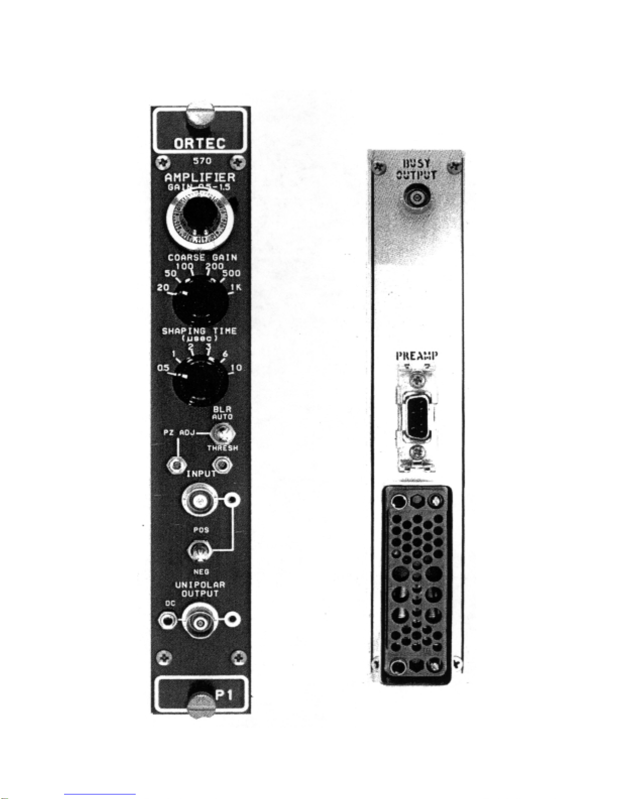
The ORTEC 570 Spectroscopy Amplifier is a
singlewidth NIM module that features a versatile
combination of switch-selectable pulse-shaping
characteristics. The amplifier has extremely low
noise, a wide gain range, and excellent overload
responseforuniversalapplicationinhigh-resolution
spectroscopy. It accepts input pulses of either
polarity that originate in germanium or silicon
semiconductor detectors, in scintillation counters
with either fast or slow scintillators, in proportional
counters, inpulsedionizationchambers,inelectron
multipliers, etc.
The 570 has an input impedance of approximately
1000
S
andacceptseitherpositiveornegativeinput
pulses with rise times <650 ns and fall times >40
:
s. Six integrate and differentiate time constants
are switch-selectable to provide optimum shaping
for resolution and count rate. The differentiation
networkhasvariablepole-zerocancellationthatcan
beadjustedtomatchpreamplifierswithdecaytimes
>40
:
s. The pole-zero cancellation drastically
reduces the undershoot after the differentiator and
greatly improves overload and count rate
characteristics.Inaddition,theamplifiercontainsan
active filter shaping network that optimizes the
signal-to-noise ratio and minimizes the overall
resolving time.
The output is unipolar and is used for spectroscopy
in systems where dc coupling can be maintained
from the 570 to the analyzer. A BLR (baseline
restorer) circuit is included in the 570 for improved
performance at all count rates. Baseline correction
is applied during intervals between input pulses
only, and a front panel switch selects a
discriminator level to identify input pulses. The
unipolar output dc level can be adjusted in the
range from -100 mV to +100 mV. This output
permits the use of the direct-coupled input of the
analyzer with a minimum amount of interface
problems.
The 570 can be used for constant-fraction timing
when operated in conjunction with an ORTEC 551,
552, or 553 Timing Single-Channel Analyzer. The
ORTEC Timing Single-Channel Analyzers feature
a minimum of walk as a function of pulse amplitude
and incorporatea variable delay time on the output
pulse to enable the timing pick-off output to be
placed in time coincidence with other signals.
The 570 has complete provisions, including power
distribution, for operating any ORTEC solid-state
preamplifier. Normally, the preamplifier pulses
should have a rise time of 0.25
:
s or less to
properly match the amplifier filter network and a
decay time greater than 40
:
s for proper pole-zero
cancellation. The 570 input impedance is 1000
S
.
Whenlong preamplifier cablesare used, the cables
can be terminated in series at the preamplifier end
or in shunt at the amplifier end with the proper
resistors. The output impedance isabout 0.1
S
,and
the output can be connected to other equipment by
a single cable going to all equipment and shunt
terminated at the far end of the cabling. See
Section 3 for further information.
1.2 POLE-ZERO CANCELLATION
Pole-zero cancellation is a method for eliminating
pulse undershoot after the differentiating network.
In an amplifier not using pole-zero cancellation
(Fig.1.1), the exponential tail on the preamplifier
output signal (usually 50 to 500
:
s) causes an
undershoot whose peak amplitude is roughly
determined from:
undershoot amplitude
differentiation time
=differentiated pulse amplitude
preamplifier pulse decay time
For a 1-
:
s differentiation time and a 50-
:
s pulse
decay timethemaximum undershoot is2%andthis
decays witha50-
:
s time constant. Under overload
conditions this undershoot is often sufficiently large
to saturate the amplifier during a considerable
portion of the undershoot, causing excessive dead
time. This effect can be reduced by increasing the
preamplifier pulse decay time (which generally
reduces the counting rate capabilities of the
preamplifier)orcompensatingfortheundershootby
causing pole-zero cancellation.

2

3
Pole-zero cancellation is accomplished by the
network shown in Fig. 1.2. The pole [s + (1/T0)] due
to the preamplifier pulse decay time is canceled by
the zero of the network [s + (k/R2C1)]. In effect, the
dc path across the differentiation capacitor addsan
attenuated replica of the preamplifier pulse to just
cancel the negative undershoot of the
differentiating network.
Total preamplifier-amplifier pole-zero cancellation
requires that the preamplifier output pulse decay
time be a single exponential decay and matched to
the pole-zero cancellation network. The variable
pole-zero cancellation network allows accurate
cancellation for all preamplifiers having 40-
:
s or
greater decay times. Improper matching of the
pole-zero network will degrade the overload per-
formance and cause excessive pileup distortion at
medium counting rates. Improper matching causes
either an undercompensation (undershoot is not
eliminated) or an overcompensation (output after
the main pulse does not return to the baseline but
decays to the baseline with the preamplifier time
constant). The pole-zero adjust is accessible on the
front panel of the 570 and can easily be adjusted by
observing the baseline on an oscilloscope with a
monoenergetic source or pulser having the same
decay time as the preamplifier under overload
conditions. The adjustment should be made so that
the pulse returns to the baseline in the minimum
time with no undershoot.
1.3 ACTIVE FILTER
When only FET gate current and drain thermal
noise are considered, the best signal-to-noise ratio
occurs when the two noise contributions are equal
for a given input pulse shape. The Gaussian pulse
shape (Fig. 1.3) for this condition requires an
amplifier with a single RC differentiate and n equal
RC integrates where n approaches infinity. The
Laplace transform of this transfer function is
G (s) = S 1
_________ x __________ (n
!
4
).
s + (1/RC) [s + (1/RC)]n
where the first factor is the single differentiate and
the secondfactor isthe nintegrates. The 570 active
filter approximates this transfer function.
Figure 1.3 illustratesthe results of pulse shaping in
an amplifier. Of the four pulse shapes shown, the
cusp would produce minimum noise but is
impractical to achieve with normal electronic and
circuitry would be difficult to measure with an ADC.
The true Gaussian shape deteriorates the
signal-to-noise ratio by only about 12% from that of
the cusp and produces a signal that is easy to
measure but requires many sections of integration
(n
6
00). With two sections of integration the
waveform identified as a Gaussian approximation
can be obtained, and this deteriorates the
signal-to-noise ratio by about 22%. The ORTEC
active filter network in the 570 provides a fourth
waveform in Fig. 1.3; this waveform has
characteristics superior to the Gaussian
approximation, yet obtains them with four complex

4
poles. By this method the output pulse shape hasa
good signal-to-noise ratio, is easy to measure, and yet requires only a practical amount of electronic
circuitry to achieve the desired results.
2 SPECIFICATIONS
2.1 PERFORMANCE
GAIN RANGE Continuously adjustable from X1
through X1500.
PULSE SHAPING Gaussian on all ranges with
peaking time equal to and pulse width at 0.1%
22.
τ
level equal to 2.9 times the peaking time.
INTEGRAL NONLINEARITY <0.05% (0.025%
typical) using 2
:
s shaping.
NOISE <8
:
V referred to the input (5
:
V typical)
using 2
:
s shaping and gain
$
100.
TEMPERATURE INSTABILITY
Gain
#
0.0075%/°C, 0 to 50°C.
DC Level <±50
:
V/°C, 0 to 50°C.
WALK
#
±3 ns for 50:1 dynamic range, including
contribution of ORTEC 551 or 552
Constant-FractionTimingSingle-ChannelAnalyzer
using 50% fraction and 0.5
:
s shaping.
COUNT RATE STABILITY The 1.33 MeV gamma
ray peak from a 60Co source, positioned at 85% of
analyzer range, typically shifts <0.024%, and its
FWHM broadens <16% when its incoming count
rate changes from 0 to 100,000 counts/s using 2
:
s
shapingandexternal pileuprejection. Theamplifier
will hold the baseline reference up to count rates in
excess of 150,000 counts/s.
OVERLOAD RECOVERY Recovers to within 2%
of rated output from X300 overload in 2.5
nonoverloaded unipolar pulse widths, using
maximum gain; same recovery from X1000
overload for bipolar pulses.
2.2 CONTROLS
GAIN Ten-turn precision potentiometer for continu-
ously variable direct-reading gain factor of X0.5 to
X1.5.
COARSE GAIN Six-position selector switch
selectsfeedback resistorsfor gain factors of 20, 50,
100, 200, 500, and 1 K.
INPUT ATTENUATOR Jumper on printed circuit
board selects an input attenuation factor of 1 or 10
(gain factor of X1 or X0.1).
POS/NEG Locking toggle switch selects input
circuit for either polarity of input pulses from the
preamplifier.
SHAPING TIME Six-position switch selects time
constant for active filter network pulse shaping;
selections are 0.5, 1, 2, 3, 6, and 10
:
s.
PZ ADJ Potentiometer to adjust pole-zero
cancellation for decay times from 40
:
s to
4
.
Factory preset at 50
:
s to match normal
characteristics of ORTEC preamplifiers.
BLR Locking toggle switch selects a source for the
gatedbaselinerestorerdiscriminatorthresholdlevel
from one of three positions.
Auto The BLR threshold is automatically set to an
optimum level asa functionof the signal noise level
by an internal circuit. This allows easy setup and
very good performance under most conditions.
PZ Adj The BLR threshold is determined by the
threshold potentiometer. The BLR time constant is
greatly increased to facilitate PZ adjustment. This
position may give the lowest noise for conditions of
<5000 counts per second and/or longer shaping
times.
Threshold The BLR threshold is set manually by
the threshold potentiometer. Range is 0 to 300 mV
referred to the positive output signal. The BLR time
constant is the same asfor the Auto switch setting.
DC ADJ Screwdriver potentiometer adjusts the
unipolar output baseline dc level; range, +100 mV
to -100 mV.
2.3 INPUT
INPUT Type BNC front panel connector accepts
either positive or negative pulses with rise times in
the range from 10 to 650 ns and decay times from
40 to 2000
:
s; Zin ~ 1000
S
, dc coupled; linear
maximum 1 V (10 V with attenuator jumper set at
X0.1); absolute maximum, 20 V.

5
2.4 OUTPUTS
UNI Unipolar front panel BNC with Zo<1
S
. Short
circuit proof; prompt, full scale linear range 0 to +10
V; active filter shaped and dc restored; dc level
adjustable to ±100 mV.
BUSY Rear panel BNC with Zo<10
S
provides a +5
V logic pulse for the duration that the input pulse
exceeds the baseline restorer discriminator level.
Connect to the ORTEC MCA Busy input for dead
time correction.
PREAMP POWER Rear panel standard ORTEC
power connector; Amphenol 17-10090; mates with
captive and non-captive power cords on all
standard ORTEC preamplifiers.
2.5 ELECTRICAL AND MECHANICAL
POWER REQUIRED (not including any load on
the Preamp Power connector)
+24 V, 80 mA; -24 V, 85 mA;
+12 V, 60 mA; -12 V, 30 mA.
FRONT PANEL DIMENSIONS NIM-standard
single-width module (1.35 by 8.714 in.) per
TID-20893 (Rev).
3 INSTALLATION
3.1 GENERAL
The 570 operates on power that must be
furnished from a NIM-standard bin and power
supply such as the ORTEC 401/402 Series. The
bin and power supply is designed for relay rack
mounting. If the equipment is to be rack mounted,
be sure that there is adequate ventilation to
prevent any localized heating of the components
that are used in the 570. The temperature of
equipment mounted in racks can easily exceed
the maximum limit of 50°C unless precautions are
taken.
3.2 CONNECTION TO POWER
The 570 contains no internal power supply and
must obtain the necessary dc operating power from
the bin and power supply in which it is installed for
operation. Always turn off power for the power
supply before inserting or removing any modules.
After all modules have been installed in the bin and
any preamplifiers have also been connected to the
Preamp Power connectors on the amplifiers, check
the dc voltage levels from the power supply to see
that they are not overloaded. The ORTEC 401/402
Series Bins and Power Supplies have convenient
test points on the power supply control panel to
permit monitoring these dc levels. If any one or
more of the dc levels indicates an overload, some
of the modules willneed to bemoved to another bin
to achieve operation.
3.3 CONNECTION TO PREAMPLIFIER
The preamplifier output signal is connected to the
570 through the Input BNC connector on the front
panel. The input impedance is about 1000
S
and is
dc-coupled to ground; therefore the preamplifier
output must be either ac-coupled or have
approximately zero dc voltage under no-signal
conditions.
The 570 incorporates pole-zero cancellation in
order to enhance the overload and count rate
characteristics of the amplifier. This technique
requires matching the network to the preamplifier
decay-time constant in order to achieve perfect
compensation.Thepole-zeroadjustmentshouldbe
set each time the preamplifier or the shaping time
constant of the amplifier is changed. For details of
the pole-zero adjustment, see Section 4.6. An
alternate method is accomplished easily byusing a
monoenergetic source and observing the amplifier
baselinewithanoscilloscopeaftereachpulseunder
approximately X2 overload conditions. Adjustment
should be made so that the pulse returns to the
baseline in a minimum amount of time with no
undershoot.
Preamplifier power at +24 V, -24 V, +12 V, and -12
V is available through thePreampPowerconnector
on the rear panel. When the preamplifier is
connected, its power requirements are obtained
from the same bin and power supply as is used for
the amplifier and this increases the dc loading on
each voltage level over and above the re-
quirements for the 570 at the module position in the
bin.

6
When the 570 is used with a remotely located
preamplifier (i.e., preamplifier-to-amplifier
connection through 25 ft or more of coaxial cable),
be careful to ensure that the characteristic
impedance of the transmission line from the
preamplifier output to the 570 input is matched.
Since the input impedance of the 570 is about
1000
S
, sending-end termination will normally be
preferred; the transmission line should be
series-terminated at the preamplifier output. All
ORTEC preamplifiers contain series terminations
that are either 93
S
or variable; coaxial cable type
RG-62/U or RG-71/U is recommended.
3.4 CONNECTION OF TEST PULSE
GENERATOR
THROUGH A PREAMPLIFIER The satisfactory
connection of a test pulse generator such as the
ORTEC 419 Precision Pulse Generator or
equivalent dependsprimarilyontwoconsiderations;
the preamplifier must be properly connected to the
570 as discussed in Section 3.3, and the proper
input signal simulation must be applied to the
preamplifier. To ensure proper input signal simu-
lation, refer to the instruction manual for the
particular preamplifier being used.
DIRECTLY INTO THE 570 Since the input of the
570 has 1000
S
of input impedance, the test pulse
generator willnormallyhavetobeterminatedatthe
amplifier input with an additional shunt resistor. In
addition, if the test pulse generator has a dc offset,
a large series isolating capacitor is also required
since the 570 input is dc coupled. The ORTEC test
pulsegeneratorsaredesignedfordirectconnection.
When any one of these units is used, it should be
terminated with a 100
S
terminator at the amplifier
input or be used with at least one of the output
attenuators set at In. (The small error due to the
finite input impedanceof the amplifier can normally
be neglected.)
SPECIAL CONSIDERATIONS FOR POLE-ZERO
CANCELLATION When a tail pulser is connected
directly to the amplifier input, the PZ ADJ should be
adjusted if overload tests are to be made (other
tests are not affected). See Section 4.6 for the
pole-zero adjustment. If a preamplifier is used and
a tail pulser is connected to the preamplifier test
input, similar precautions are necessary. In this
case the effect of the pulser decay must be re-
moved; i.e., a step input should be simulated.
3.5 SHAPING CONSIDERATIONS
The shaping time constant on the 570 is
switch-selectable in steps of 0.5, 1, 2, 3, 6, and
10
:
s. The choice of the proper shaping time
constant is generally a compromise between
operating at a shorter time constant for accom-
modation of high counting rates and operating with
a longer time constant for a better signal-to-noise
ratio. For scintillation counters, the energy
resolution depends largely on the scintillator and
photomultiplier, and therefore a shaping time
constant of about four times the decay-time
constant of the scintillator is a reasonable choice
(for Nal, a 1-
:
s shaping time constant is about
optimum). For gas proportional counters, the
collection time is normally in the 0.5 to 5
:
s range
and a 2-
:
s or greater time constant selection will
generally give optimum resolution. For surface
barrier semiconductor detectors, a 0.5- to 2-
:
s
resolving time will generally provide optimum
resolution. Shaping time for Ge(Li) detectors will
vary from 1 to 6
:
s, depending on the size,
configuration, and collection time of the specific
detectorandpreamplifier.Whenacharge-sensitive
preamplifier is used, the optimum shaping time
constant to minimize the noise of a system can be
determined by measuring the output noise of the
system anddividingit by the system gain. Since the
570hasalmostconstant gain for all shapingmodes,
the optimum shaping can be determined by
measuring the output noise of the 570 with a
voltmeter as each shaping time constant is
selected.
3.6 LINEAR OUTPUT CONNECTIONS AND
TERMINATING CONSIDERATIONS
Since the 570 unipolar output is normally used for
spectroscopy, the 570 is designed with a great
amount of flexibility in order for the pulse to be
interfaced with an analyzer. A gated baseline
restorer (BLR) circuit is included in this output for
improved performance at all count rates. A switch
on the front panel permits the threshold for the
restorer gate to be determined automatically,
according to the input noise level, or manually, with
a screwdriver adjustment. The switch also has a
center PZ ADJ setting that can be used to eliminate
theBLReffectwhenmakingpole-zeroadjustments.
The unipolar output dc level can be adjusted from
!
0.1 to +0.1 V to set the zero intercept on the
analyzer when direct coupling is used.
Three general methods of termination are used.
The simplest of these is shunt termination at the
receiving end of the cable. A second method is
series terminationat the sending end. The third isa
combination of series and shunt termination, where
the cable impedance is matched both in series at
the sending end and in shunt at the receiving end.

7
The combinationismost effective, but this reduces
the amount of signal strength at the receiving end
to 50% of that which is available in the sending in-
strument.
To use shunt termination at the receiving end of the
cable, connect the output on the 570 front panel
through 93
S
cable to the input of the receiving
instrument.ThenuseaBNCteeconnectortoattach
both the interconnecting cable and a 100
S
terminator at the input connector of the receiving
instrument. Since the input impedance of the
receiving instrument is normally 1000
S
or more,
the effective instrument input impedance with the
100
S
terminatorwillbeof theorderof 93
S
and this
will match the cable impedance correctly.
For customer convenience, ORTEC stocks the
proper terminators and BNC tees, or they can be
ordered from a variety of commercial sources.
3.7 SHORTING OR OVERLOADING THE
AMPLIFIER OUTPUT
The 570 output is dc coupled with an output
impedance of about 0.1
S
. If the output is shorted
with a direct short circuit the output stage will limit
the peak current of the output so that the amplifier
will not be harmed. When the amplifier is
terminated with 100
S
, the maximum rate allowed
to maintain the linear output is
200 000 cps 10
-------------------- x ---------- .
(
:
S) V0(V)
τ
3.8 BUSY OUTPUT CONNECTION
The signal through the rear panel Busy output
connector rises from 0 to about +5 V at the onset of
each linear input pulse. Its width is equal to the time
the input pulse amplitude exceeds the BLR
discriminator level. It can be used to provide MCA
dead time correction, to control the generation of
input pulses, to observe normal operation with an
oscilloscope, or for any of a variety of other ap-
plications. Its use is optional and no termination is
required if the output is not being used.
4 OPERATION
4.1 INITIAL TESTING AND OBSERVATION
OF PULSE WAVEFORMS
Refer to Section 6 for information on testing
performance and observing waveforms at front
panel test points. Figure 4.1 shows some typical
unipolar output waveforms.
4.2 FRONT PANEL CONTROLS
GAIN A Coarse Gain switch and a Gain 10-turn
lockingprecisionpotentiometerselectandprecisely
adjust the gain factor for the amplification in the
570. Switch settings are X20, 50, 100, 200, 500,
and 1000. Continuous fine gain range is from X0.5
to X1.5, using markings of 500 through 1500 dial
divisions. An internal jumper setting provides one
additional gain factor selection of either X1.0 or
X0.1. Collectively the range of gain can be set at
any level from X1.0 through X1500, using all three
of these controls.
POS/NEG A locking toggle switch selects an input
circuitthatacceptseitherpolarity of pulsesfrom the
preamplifier.
PZ ADJ A screwdriver control to set the pole-zero
cancellation to match the preamplifier pulse decay
characteristics. The range is from 40
:
s to 00.
DC ADJ A screwdriver control adjusts the dc
baseline level of the unipolar output in the range of
-0.1 V to +0.1 V.
SHAPING A 6-position switch selects equal
integrate and differentiate time constants to shape
the input pulses. Settings are 0.5, 1, 2, 3, 6, and 10
:
s.

8
BLR A 3-positionlockingtoggle switchcontrolsthe
operation of the internal baseline restorer (BLR)
circuit.
The center setting of the switch is effectively Off,
and this permits adjustment of the PZ ADJ control
without interference from the BLR circuit. The Auto
setting of the switch selects a circuit that regulates
the threshold of the BLR gate according to the
output noise level. The Threshold setting permits
manual control of the BLR gatethreshold, using the
screwdriver control immediately below the toggle
switch.
4.3 FRONT PANEL CONNECTORS
INPUT Accepts input pulses to be shaped and/or
amplified by the 570. Compatible characteristics;
positive or negative with rise time from 10 to 650
ns; decay time greater than 40
:
s for proper
pole-zerocancellation;inputlinearamplituderange
0 to 10 V, with a maximum limit of ±20 V. Input
impedance is approximately 1000
S
.
UNIPOLAR OUTPUT Provides a unipolar positive
output with characteristics that are related to input
peak amplitude, gain, shaping time constants,
pole-zero cancellation, and baseline stabilization.
The dc baseline level isadjustable for offset to ±0.1
V. Output impedance through this connector is
about 0.1
S
, dc coupled. Linear range 0 to +10 V.
4.4 REAR PANEL CONNECTORS
BUSYProvidesasignal thatrisestoapproximately
+5 V for the time that the input pulse amplitude
exceeds the BLR discriminator level, which can be
controlled manually or automatically. The output
can be used to correct for dead time in the ORTEC
MCA by connecting it to the MCA Busy input.
PREAMP Providespowerconnectionsfrom thebin
and power supply to the ORTEC preamplifier. The
dc levels include +24 V, -24 V, +12 V, and -12 V.
4.5 STANDARD SETUP PROCEDURE
a. Connect the detector, preamplifier, high voltage
powersupply,andamplifier intoabasicsystem and
connect the amplifier output to an oscilloscope.
Connect the preamplifier power cable to the
Preamp connector on the 570 rear panel. Turn on
power in the bin and power supply and allow the
electronics of the system to warm up and stabilize.

9
b. Set the 570 controls initially as follows:
Shaping 2
:
s
Coarse Gain 50
Gain 1.000
Internal Jumper X1.0 (factory installed
position)
BLR PZ ADJ
Thresh Fully clockwise
Pos/Neg Match input pulse polarity
c. Use a 60CO calibration source; place it about 25
cm from the active face of the detector. The
unipolar output pulse from the 570 should be about
8 to 10 V, using a preamplifier with a conversion
gain of 170 mV/MeV.
d.Readjust the Gaincontrol so that thehigherpeak
from the 60CO source (1.33 MeV) provides an
amplifier output at about 9 V.
4.6 POLE-ZERO ADJUSTMENT
The pole-zero adjustment is extremely critical for
good performance at high count rates. This
adjustmentshould becheckedcarefullyforthebest
possible results.
USING A GERMANIUM SYSTEM AND 60CO
a. Adjust the radiation source count rate between 2
kHz and 10 kHz.
b. Observe the unipolar output with an
oscilloscope. Adjust the PZ ADJ control so that the
trailing edge of the pulses returns to the baseline
without overshoot or undershoot (see Fig. 4.2).
The oscilloscope used must be dc coupled and
must not contribute distortion in the observed
waveforms. Oscilloscopes such as Tektronix 453,
454, 465, and 475 will overload for a 10-V signal
when the vertical sensitivity is less than 100
mV/cm. To prevent overloading the oscillbscope,
use the clamp circuit shown in Fig. 4.3.
USING SQUARE WAVE THROUGH
PREAMPLIFIER TEST INPUT
Amoreprecisepole-zero adjustment inthe570can
be obtained by using a square wave signal as the
input to the preamplifier. Many oscilloscopes
include a calibration output on the front panel and
this is a good source of square wave signals at a
frequency of about 1 kHz. The amplifier
differentiates the signal from the preamplifier so
that it generates output signals of alternate
polarities on the leading and trailing edges of the
square wave input signal, and these can be

10
compared as shown in Fig. 4.4 to achieve excellent
pole-zero cancellation. Use the following
procedure:
a. Remove all radioactive sources from the vicinity
of the detector. Set up the system as for normal
operation, including detector bias.
b. Set the 570controlsasfor normal operation; this
includes gain, shaping, and input polarity.
c. Connect the source of 1-kHz square waves
through an attenuator to the Test input of the
preamplifier. Adjust the attenuator so that the
570 output amplitude is about 9 V.d. Observe the
Unipolar output of the 570 with an oscilloscope,
triggered from the 570 Busy output. Adjust the PZ
ADJ control for proper response according to Fig.
4.4. Use the clamp circuit or Fig. 4.3 to prevent
overloading the oscilloscope input.
Figure 4.4A. shows the amplifier output as a series
ofalternatepositiveandnegativeGaussianpulses.
In the other three pictures of this figure, the
oscilloscope was triggered to show both positive
andnegativepulsessimultaneously. Thesepictures
show more detail to aid in proper adjustment.

11
4.7 BLR THRESHOLD ADJUSTMENT
After the amplifier gain and shaping have been
selected and the PZ ADJ control has been set to
operate properly for the particular shaping time,
the BLR Thresh control can be used to establish
the correct discriminator threshold for the
baseline restorer circuit. Normally, the toggle
switch can be set at Auto, and the threshold level
will be set automatically just above the noise
level. If desired, the switch can be set at
Threshold and the manual control just below the
switch can then be used to select the level
manually as follows:
a. Remove all radioactive sources from the vicinity
of the detector. Set up the system as for normal
operation, including detector bias.
b. Set the BLR switch at Threshold and turn the
control fully clockwise, for 300 mV.
c. Observe the unipolar output on the 100 mV/cm
scale of the oscilloscope, using 5
:
s/cm horizontal
deflection. Trigger the oscilloscope with the Busy
output from the 570.
d. Reduce the control setting until the baseline
discriminator begins to trigger on noise; this
corresponds to about 200 counts/s from the Busy
output. Adjust the trigger level according to the
information in Fig. 4.5.
If a ratemeter or counter-timer is available, it can
be connected to the Busy output and the threshold
level can then be adjusted for about 200 counts/s.

12
4.8 OPERATION WITH SEMICONDUCTOR
DETECTORS
CALIBRATION OF TEST PULSER An ORTEC
419 Precision Pulse Generator, or equivalent, is
easily calibrated so that the maximum pulse height
dial reading (1000 divisions) is equivalent to
10-MeV loss in a silicon radiation detector. The
procedure is as follows:
a. Connect the detector to be used to the
spectrometer system; i.e., preamplifier, main
amplifier, and biased amplifier.
b. Allow excitation from a source of known energy
(for example, alpha particles) to fall on the
detector.
c. Adjust the amplifier gain and the bias level of the
biased amplifier to give a suitable output pulse.
d. Set the pulser Pulse Height control at the energy
of the alpha particles striking the detector (for
example, set the dial at 547 divisions for a 5.47-
MeV alpha particle energy).
e. Turn on the pulser and use its Normalize control
and attenuators to set the output due to the pulser
for the same pulse height as the pulse obtained in
step c. Lock the Normalize control and do not
move it again until recalibration is required.
The pulser is now calibrated; the Pulse Height dial
reads directly in MeV if the number of dial divisions
is divided by 100.
AMPLIFIER NOISE AND RESOLUTION
MEASUREMENTS As shown in Fig. 4.6, a
preamplifier, amplifier, pulse generator,
oscilloscope, andwide-band rms voltmeter suchas
the Hewlett-Packard 3400A are required for this
measurement. Connect a suitable capacitor to the
input to simulate the detector capacitance desired.
To obtain the resolution spread due to amplifier
noise:
a. Measure the rms noise voltage (Erms) at the
amplifier output.
b. Turn on the 419 Precision Pulse Generator and
adjust thepulseroutput toany convenient readable
voltage,Eo,asdeterminedby theoscilloscope.The
full width at half maximum (FWHM) resolution
spread due to amplifier noise is then
2.35 Erms Edial
N(FWHM) = ----------------------------------
Eo
where Edial is the pulser dial reading in MeV and
2.35 is the factor for rms to FWHM. For
average-responding voltmeters such as the
Hewlett-Packard 400D, the measured noise must
be multiplied by 1.13 to calculate the rms noise.
The resolution spread will depend on the total input
capacitance, since the capacitance degrades the
signal-to-noise ratio much faster than the noise.
DETECTOR NOISE-RESOLUTION
MEASUREMENTS The measurement just
described can be made with a biased detector
insteadof the external capacitor that would beused
to simulate detector capacitance. The resolution
spread will be larger because the detector
contributesbothnoiseandcapacitancetotheinput.
The detector noise-resolution spread can be
isolated from the amplifier noise spread if the
detector capacity is known, since
(Ndet)2+ (Namp)2= (Ntotal)2,
where Ntotal is the total resolution spread and Namp is
the amplifier resolution spread whenthe detector is
replaced by its equivalent capacitance.
The detector noise tends to increase with bias
voltage, but the detector capacitance decreases,
thus reducing the resolution spread. The overall
resolution spread will depend upon which effect is
dominant. Figure 4.7 shows curves of typical
noise-resolution spread versus bias voltage, using
data from several ORTEC silicon surface barrier
semiconductor radiation detectors.

13
AMPLIFIER NOISE-RESOLUTION
MEASUREMENTSUSINGMCAProbablythemost
convenient method of making resolution
measurements is with a pulse height analyzer as
shown by the setup illustrated in Fig. 4.8.
The amplifier noise-resolution spread can be
measured directly with a pulse height analyzer and
the mercury pulser as follows:
a. Select the energy of interest with anORTEC419
Precision Pulse Generator. Set the amplifier and
biased amplifier gain andbiaslevel controls so that
the energy is in a convenient channel of the
analyzer.
b. Calibrate the analyzer in keV per channel, using
the pulser; full scale on the pulser dial is 10 MeV
when calibrated as described above.
c. Obtain the amplifier noise-resolution spread by
measuring the FWHM of the pulser peak in the
spectrum.
The detector noise-resolution spread for a given
detector bias can be determined in the same
manner by connecting a detector to the
preamplifier input. The amplifier noise-resolution
spread must be subtracted as described in
"Detector Noise-Resolution Measurements." The
detector noise will vary with detector size and bias
conditions and possibly with ambient conditions.
CURRENT-VOLTAGEMEASUREMENTSFORSi
AND Ge DETECTORS The amplifier system is not
directly involved in semiconductor detector
current-voltage measurements, but the amplifier
serves to permit noise monitoring during the setup.
The detector noise measurement is a more
sensitive method than a current measurement of
determining the maximum detector voltage that
should be used because the noise increases more
rapidly than the reverse current at the onset of
detectorbreakdown.Makethismeasurement in the
absence of a source.
Figure 4.9 shows the setup required for
current-voltage measurements. An ORTEC 428
Bias Supply is used as the voltage source. Bias
voltage should be applied slowly and reduced
when noise increases rapidly as a function of
applied bias. Figure 4.10 shows several typical
current voltage curves for ORTEC silicon
surface-barrier detectors.
When it is possible to float the microammeter at
the detector bias voltage, the method of detector
current measurement shown by the dashed lines in

14
Fig. 4.9 is preferable. The detector is grounded as
in normal operation and the microammeter is
connectedtothecurrent monitoringjackon the428
Detector Bias Supply.
4.9 OPERATION IN SPECTROSCOPY
SYSTEMS
HIGH-RESOLUTION ALPHA-PARTICLE
SPECTROSCOPYSYSTEMTheblockdiagram of
a high-resolution spectroscopy system for
measuring natural alpha particle radiation is shown
in Fig. 4.11. Since natural alpha radiation occurs
only above several MeV, an ORTEC 444 Biased
Amplifier is used to suppress the unused portion of
the spectrum; the same result can be obtained by
using digital suppression on the MCA in many
cases. Alphaparticle resolution is obtained in the
following manner:
a. Use appropriate amplifier gain and minimum
biased amplifier gain and bias level. Accumulate
the alpha peak in the MCA.
b. Slowly increase the bias level and biased
amplifier gain until the alpha peak is spread over 5
to 10 channels and the minimum-to
maximum-energyrangedesiredcorrespondstothe
first and last channels of the MCA.
c. Calibrate the analyzer in keV per channel using
the pulser and the known energy of the alpha peak
(see "Calibration of Test Pulser") or two
known-energy alpha peaks.
d. Calculate the resolution by measuring the
number of channelsat the FWHM level in thepeak
and converting this to keV.
HIGH-RESOLUTION GAMMASPECTROSCOPY
SYSTEM A high-resolution gamma spectroscopy
system block diagram is shown in Fig. 4.12.
Although a biased amplifier is not shown (an
analyzer with more channels being preferred), it
can be used if the only analyzer available has
fewer channels and only higher energies are of
interest.
When germanium detectors that are cooled by a
liquid nitrogen cryostat are used, it is possible to
obtain resolutions from about 1 keV FWHM up
(depending on the energy of the incident radiation
and the size and quality of the detector).
Reasonable care is required to obtain such results.
Some guidelines for obtaining optimum resolution
are:
a. Keep interconnection capacitiesbetweenthede-
tector andpreamplifier to anabsoluteminimum (no
long cables).
b.Keephumiditylownearthedetector-preamplifier
junction.

15
c. Operate the amplifier with the shaping time that
provides the best signal-to-noise ratio.
d. Operate at the highest allowable detector bias to
keep the input capacity low.
SCINTILLATION-COUNTER GAMMA
SPECTROSCOPY SYSTEMS The ORTEC 570
can be used in scintillation-counter spectroscopy
systems as shown in Fig. 4.13. The amplifier
shaping time constants should be selected in the
region of 0.5 to 1
:
s for Nal or plastic scintillators.
For scintillators having longer decay times, longer
time constants should be selected.
X-RAY SPECTROSCOPY USING
PROPORTIONAL COUNTERS Space charge
effects in proportional counters, operated at high
gas amplification, tend to degrade the resolution
capabilities drastically at x-ray energies, even at
relatively low counting rates. By using a high-gain
low-noise amplifying system and lower gas
amplification, these effects can be reduced and a
considerable improvement in resolution can be
obtained.
The block diagram in Fig. 4.14 shows a system of
this type. Analysis can be accomplished by
simultaneous acquisition of all data on a
multichannel analyzer or counting a region of
interest in a single-channel analyzer windowwith a
counter and timer or counting ratemeter.
4.10 OTHER EXPERIMENTS
Block diagrams illustrating how the 570 and other
ORTEC modules can be used for experimental
setups for various other applications are shown in
Figs. 4.15, 4.16, and 4.17.
Table of contents
Other ORTEC Amplifier manuals