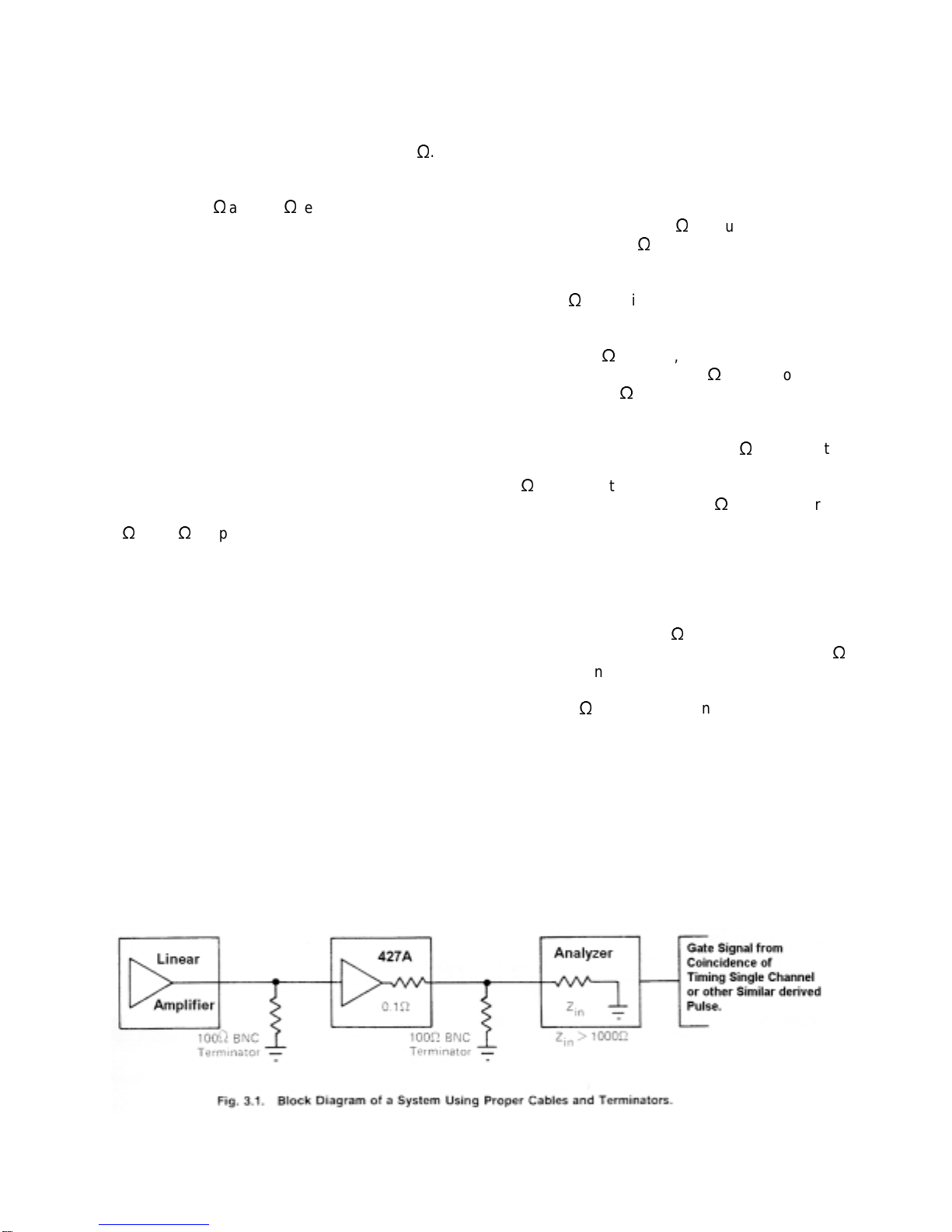
ORTEC 427A Service manual

Model 427A
Delay Amplifier
Operating and Service Manual
This manual Applies to instruments marked
“Rev 22" on rear panel
Printed in U.S.A. ORTEC®Part No. 733210 1202
Manual Revision B

Advanced Measurement Technology, Inc.
a/k/a/ ORTEC®, a subsidiary of AMETEK®, Inc.
WARRANTY
ORTEC* warrants that the items will be delivered free from defects in material or workmanship. ORTEC makes
no other warranties, express or implied, and specifically NO WARRANTY OF MERCHANTABILITY OR
FITNESS FOR A PARTICULAR PURPOSE.
ORTEC’s exclusive liability is limited to repairing or replacing at ORTEC’s option, items found by ORTEC to
be defective in workmanship or materials within one year from the date of delivery. ORTEC’s liability on any
claim of any kind, including negligence, loss, or damages arising out of, connected with, or from the performance
or breach thereof, or from the manufacture, sale, delivery, resale, repair, or use of any item or services covered
by this agreement or purchase order, shall in no case exceed the price allocable to the item or service furnished
or any part thereof that gives rise to the claim. In the event ORTEC fails to manufacture or deliver items called
for in this agreement or purchaseorder, ORTEC’sexclusiveliabilityand buyer’s exclusive remedy shallberelease
of the buyer from the obligation to pay the purchase price. In no event shall ORTEC be liable for special or
consequential damages. Quality Control
Before being approved for shipment, each ORTEC instrument must pass a stringent set of quality control tests
designed to expose any flaws in materials or workmanship. Permanent records of these tests are maintained for
use in warranty repair and as a source of statistical information for design improvements.
Repair Service
If it becomes necessary to return this instrument for repair, it is essential that Customer Services be contacted in
advance of its return so that a Return Authorization Number can be assigned to the unit. Also, ORTEC must be
informed, either in writing, by telephone [(865) 482-4411] or by facsimile transmission[(865) 483-2133], of the
nature of the fault of the instrument being returned and of the model, serial, and revision ("Rev" on rear panel)
numbers. Failure to do so may cause unnecessary delays in getting the unit repaired. The ORTEC standard
procedure requires that instruments returned for repair pass the same quality control tests that are used for
new-production instruments. Instruments that are returned should be packed so that they will withstand normal
transit handling and must be shipped PREPAID via Air Parcel Post or United Parcel Service to the designated
ORTEC repair center. The address label and the package should include the Return Authorization Number
assigned. Instruments being returned that are damaged in transit due to inadequate packing will berepaired at the
sender's expense, and it will be the sender's responsibility to make claim with the shipper. Instruments not in
warranty should follow the same procedure and ORTEC will provide a quotation.
Damage in Transit
Shipments should be examinedimmediately upon receiptfor evidenceofexternal or concealeddamage. Thecarrier
making deliveryshouldbenotifiedimmediatelyof anysuchdamage, sincethecarrier is normallyliablefor damage
in shipment. Packing materials, waybills, and other such documentation should be preserved in order to establish
claims. After such notification to the carrier, please notify ORTEC of the circumstances so that assistancecan be
provided in making damage claims and in providing replacement equipment, if necessary.
Copyright © 2002, Advanced Measurement Technology, Inc. All rights reserved.
*ORTEC®is a registered trademark of Advanced Measurement Technology, Inc. All other trademarks used
herein are the property of their respective owners.

iii
CONTENTS
WARRANTY ....................................................................... ii
SAFETY INSTRUCTIONS AND SYMBOLS ............................................... iv
SAFETY WARNINGS AND CLEANING INSTRUCTIONS ..................................... v
1. DESCRIPTION................................................................... 1
2. SPECIFICATIONS ................................................................ 1
2.1. PERFORMANCE ............................................................. 1
2.2. CONTROLS................................................................. 2
2.3. INPUTS .................................................................... 2
2.4. OUTPUTS .................................................................. 2
2.5. POWERREQUIRED .......................................................... 2
3. INSTALLATION .................................................................. 2
3.1. GENERAL .................................................................. 2
3.2. CONNECTIONTOPOWER..................................................... 2
3.3. SIGNAL CONNECTIONS TO 427A ............................................... 2
3.4. LINEAROUTPUTSIGNALCONNECTIONSANDTERMINATINGIMPEDANCE............. 3
4. OPERATING INSTRUCTIONS ....................................................... 4
4.1. INITIAL TESTING AND OBSERVATION OF PULSE WAVEFORMS ...................... 4
4.2. CONNECTORDATA .......................................................... 4
4.3. TYPICALOPERATINGCONSIDERATIONS ........................................ 4
5. MAINTENANCE.................................................................. 4
5.1. TESTINGPERFORMANCEOFTHEDELAYAMPLIFIER.............................. 4
5.2. CHANGINGTHEAMPLIFIERGAIN............................................... 5
5.3. SUGGESTIONSFORTROUBLESHOOTING ....................................... 5
5.4. FACTORY REPAIR ........................................................... 5

iv
SAFETY INSTRUCTIONS AND SYMBOLS
This manual contains up to three levels of safety instructions that must be observed in order to avoid
personal injury and/or damage to equipment or other property. These are:
DANGER Indicates a hazard that could result in death or serious bodily harm if the safety instruction is
not observed.
WARNING Indicates a hazard that could result in bodily harm if the safety instruction is not observed.
CAUTION Indicates a hazard that could result in property damage if the safety instruction is not
observed.
Please read all safety instructions carefully and make sure you understand them fully before attempting to
use this product.
In addition, the following symbol may appear on the product:
ATTENTION – Refer to Manual
DANGER – High Voltage
Please read all safety instructions carefully and make sure you understand them fully before attempting to
use this product.

v
DANGER Opening the cover of this instrument is likely to expose dangerous voltages. Disconnect the
instrument from all voltage sources while it is being opened.
WARNING Using this instrument in a manner not specified by the manufacturer may impair the
protection provided by the instrument.
CAUTION To prevent moisture inside of the instrument during external cleaning, use only enough liquid
to dampen the cloth or applicator.
SAFETY WARNINGS AND CLEANING INSTRUCTIONS
Cleaning Instructions
To clean the instrument exterior:
!
Unplug the instrument from the ac power supply.
!
Remove loose dust on the outside of the instrument with a lint-free cloth.
!
Remove remaining dirt with a lint-free cloth dampened in a general-purpose detergent and water
solution. Do not use abrasive cleaners.
!
Allow the instrument to dry completely before reconnecting it to the power source.

vi

1
ORTEC MODEL 427A
DELAY AMPLIFIER
NOTICE
Slideswitches areusedinthe427Atoselect thedesired amountof signaldelay. Thecontacts of theseswitches arecoated
with alubricant toprevent them from oxidizing. If this lubricant is removed from aportion of the contact, oxidation will occur
and madeit difficult for the switches to make contact properly. If a switch does not make contact, thesignal will either not
appear at the output or appear at a reduced amplitude. When the switches do not make contact, simply operate them a few
times; this will remove the oxide and restore the contacts to their proper state.
1. DESCRIPTION
The ORTEC 427A Delay Amplifier has a nominal
gain of unity and can delay a linear or logic signal
from zero to 4.75
:
s in 0.25-
:
s increments. The
amount of delay is selected by five front panel
switches. This delay is accomplished by inserting
any combination of five delay lines of .025, 0.5, 1.0;
1.0 and 2.0
:
s in series with the signal path. These
delay lines are terminated in their characteristic
impedances at both ends to minimize impedance
mismatching and resultant pulse reflections on the
lines.
The 427A features a gain of 1 from the input to the
output. It iscompletely dc-coupled from theinput to
the output, which permits the delay amplifier to be
used in high count rate circuits with excellent
fidelity. Any required baseline restoration may be
accomplished at the most convenient place, either
before or after the 427A.
NOTE: The 427A has a limited bandwidth asshown
in theSpecifications.Consequently,thisinstrument
should not be used to delay signals of varying
bandwidth. Such signals are obtained when a
biased amplifier without a stretcher is used
following a shaping amplifier. The ORTEC 444
Biased Amplifier has an internal stretcher that
precedes thebiased amplifier sectionand therefore
produces constant bandwidth signals. In older
spectroscopy systemsusing a biased amplifier and
stretcher (the 408 and 411) the droop of the
stretched output was so large that the biased
amplifier had to be used before the stretcher. In
these systemsthe 427A should followthe stretcher
in the signal path.
2. SPECIFICATIONS
2.1. PERFORMANCE
GAIN Unity ±2% at zero delay.
GAIN VARIATION WITH DELAY ±10%,
!
2% for
any combination of delays (bipolar pulse, 0.5
:
s
shaping time).
FEEDTHROUGH AND DELAY RIPPLE <2%
(bipolar pulse, 0.5
:
s shaping time).
PROPAGATION DELAY 200 ns typical.
DELAY LINE TOLERANCES ±5%.
RISE TIME AND BANDWIDTH AS A FUNCTION
OF DELAY
Delay
(
:
S) Maximum
Rise Time
(ns)
Minimum
Bandwidth
(MHZ)
0 280 1.25
0.25 280 1.25
0.5 290 1.20
1.0 310 1.13
2.0 340 1.03
3.0 360 0.972
4.0 370 0.945
4.5 380 0.920
4.75 400 0.875

2
INTEGRAL NONLINEARITY <±0.05%, 0 to
+10 V.
TEMPERATURE INSTABILITY Gain shift of the
amplifier is <±0.01% per °C; additional shift of
!
0.013% per °C should be expected for each
microsecond of delay used; operating temperature
range, 0 to 50°C.
2.2. CONTROLS
LINEAR DELAY Any combination of the following:
0.25, 0.5, 1.0, 1.0, and 2.0
:
s; maximum 4.75
:
s.
DC OUTPUT LEVEL ADJ ±1 V.
DC OUTPUT LEVEL INSTABILITY <0.1 mV/°C.
INPUT AND OUTPUT CONNECTORSBNC; types
UG-1094/U and UG-1094A/U.
2.3. INPUTS
POLARITY Either positive or negative.
SIGNAL SPAN ±10 V linear range.
IMPEDANCE >1k
S
, dc-coupled.
2.4. OUTPUTS
There are 2 outputs, each with a linear range of 0 to
±10 V, 0 to ±11 V maximum.
IMPEDANCE <0.1
S
dc-coupled, short-circuit
protected, front panel BNC; 93
S
dc-coupled, rear
panel BNC.
2.5. POWER REQUIRED
+24 V, 30 mA;
!
24 V, 30 mA.
3. INSTALLATION
3.1. GENERAL
The 427A is used in conjunction with an ORTEC
4001/402 Series Bin and Power Supply, which is
intended for rack mounting; therefore if vacuum
tube equipment is operated in the same rack with
the 427A, there must be sufficient cooling by
circulating air to prevent any localized heating of
the all-transistor circuitry used through out the
module. The equipment mounted in racks should
not be subjected to temperatures in excess of
120°F (50°C).
3.2. CONNECTION TO POWER
Since the 427A contains no internal power supply,
it must obtain power from a Nuclear Standard Bin
and Power Supply such as the 4001A/402A. It is
recommended the Bin Power Supply be turned off
when modules are inserted or removed. ORTEC
modules are designed so that the Bin Power Supply
cannot be overloaded even when there is a full
complement of modules in the Bin. Since this may
not be true, however, when the Bin contains
modules other than those of ORTEC design, the
Power Supply voltages should be checked after
modules are inserted. The 4001A/402A has test
pointson the Power Supply control panel to monitor
the dc voltages.
When using the 427A outside the 4001A/402A Bin
and Power Supply, be sure that the jumper cable
used properly accounts for the power supply
grounding circuits provided in the recommended
AEC standards of TID-20893 (Rev). Both high-
quality and power-return ground connections are
provided to ensure proper reference voltage
feedback into the power supply, and they must be
preserved in remote cable installations. Care must
also be exercised to avoid ground loops when the
module is not operated in the Bin.
3.3. SIGNAL CONNECTIONS TO 427A
The 427A input is compatible with all linear output
signalsof ORTEC modular electronic instruments.
The medium-speed logic pulse of these
instruments is also suitable for use with the 427A;
however, the rise time of logic pulse will be
increased considerably because of the limited
bandwidth of the 427A. (See Specifications for
bandwidth and rise time vs delay.) The signal
range of the input is from 0 to 10 V. The input
pulse shape can be as narrow as 300 to 400 ns or
as long as infinity.
The connecting coaxial cableshouldbeterminated
in its characteristic impedance at the input
connector when cable lengths exceed

3
approximately 4 ft (see Fig. 3.1). The input
impedance of the 427A is approximately 1100
S
. It
is recommended that RG-62/U or RG-63/U coaxial
cable be used because of their relatively high
impedanceof 93
S
and125
S
respectively.Baseline
restoration will normally be accomplished in the
linear amplifier. The input dc level furnished into
the 427A should be zero with no signal present, and
thiswill normally be adjusted in the linear amplifier
output. The 427A has a dc-coupled output with a
dc-level adjustment for a range of ±1 V. This
permits the input to the analyzer to be normalized
in order to establish its zero-energy crossover
calibration.
3.4. LINEAR OUTPUT SIGNAL
CONNECTIONS AND TERMINATING
IMPEDANCE
The source impedance of the 0- to 10-V standard
linear outputs of most ORTEC instruments is
furnished through a series impedance of either
0.1
S
or 93
S
, depending on the connector that is
used for the connection to the next module. When
the interconnecting cable is short, such as
maximum of 4 ft, this will not usually result in any
interference problems even though impedance
matching is disregarded. However, if acablelonger
than approximately 4 ft. is necessary in a linear
output, it should be terminated in a resistive load
equal to the impedance in order to prevent
oscillations.
Therearethreegeneral methodsof terminationthat
are used. The simplest of these is shunt termination
at the receiving end of the cable. A second method
is series termination at the sending end. Thethirdis
a combination of series and shunt termination,
where the cable impedance is matched both in
series at the sending end and in shunt at the
receiving end. The most effective method is the
combination, but termination by this method
reduces the amount of signal strength at the
receiving end to 50% of that which is available in
the sending instrument.
To use shunt termination at the receiving end of
the cable, connect the 1
S
output of the sending
device through 93
S
cable to the input of the
receiving instrument. Then use a BNC tee
connector accept both the interconnecting cable
and 100
S
resistive terminator at the input
connector of the receiving instrument. Since the
input impedance of the receiving instrument is
normally 1000
S
or more, the effective instrument
input impedance with the 100
S
terminator will be
of the order of 93
S
, and this correctly matches the
cable impedance.
For series termination, use the 93
S
output of the
sending instrument for the cable connection. Use
93
S
cable to interconnect thisinto the input of the
receivinginstrument. The1000
S
(or more) normal
input impedance at the input connector represents
an essentially open circuit, and the series
impedance inthesendinginstrumentnowprovides
the proper termination for the cable.
For the combination of series and shunt
termination, use the 93
S
output of the sending
instrument for the cable connection and use 93
S
cable. Attheinput for thereceivinginstrument,use
a BNCtee to accept both the interconnecting cable
and a 100
S
resistive terminator. Note that the
signal span at the receiving end of this type of
receiving circuit will always be reduced to 50% of
the signal span furnished by the sending
instrument.
For your convenience, ORTEC stocks the proper
terminators and BNC tees, or you can obtain them
from a variety of commercial sources.

4
4. OPERATING INSTRUCTIONS
4.1. INITIAL TESTING AND OBSERVATION
OF PULSE WAVEFORMS
Refer to Section 5.1 of this manual for information
concerning testing performance and observing
pulse waveforms.
4.2. CONNECTOR DATA
INPUT
The INPUT BNC connector accepts the incoming
pulse that is delayed (temporarilystored) in passing
through the amplifier. The input impedance is
approximately 1100
S
dc-coupled. The dc level of
the signal line furnished to the input of the 427A
should be adjusted to zero volts when no signal is
present on the line. The input voltage rated range is
0 to ±10 V, and the voltage gain in nominally unity.
OUTPUT
There are two OUTPUT BNC connectors, one on
the front panel and one on the rear panel. The
output driving impedance for the front panel
connection is approximately 0.1
S
and it is short-
circuit protected. The connector on the rear panel
furnishes the same output through a 93
S
series
impedance. The dcoutput level isadjustable with a
front panel screwdriver control for a range of ±1 V
to normalizeit for thenext instrument into which the
signal isbeing furnished, and both the 1
S
and 93
S
outputs are dc-coupled. The output test point is a
convenient location for checking the dc output level
with a voltmeter or an oscilloscope.
4.3. TYPICAL OPERATING
CONSIDERATIONS
There is a propagation delay in the 427A of
approximately 200 ns. This delay is present
betweentheinputandoutputconnectorswhenallof
the delay switches are set at OUT and is added to
any delay that is switched in during operation.
The 427A is typically used in a linear system after
the main pulse-shaping amplifier. It is also directly
compatible with, and can be driven from, any
ORTEC linear output circuit. The input and output
signal range is rated from 0 to 10 V, positive or
negative. After the desired amount of delay has
been selected, the 427A output should be checked
with an oscilloscope to ensure that the dynamic
range of the unit is not exceeded. The gain of the
427A is nominally unity, but in increases to
approximately 1.1 when all of thedelay (4.75
:
s) is
selected.
5. MAINTENANCE
The testing instructions given here and the circuit
descriptionsin Section 5 should provide assistance
in locating the region of trouble and in remedying
the malfunction. The information given in Section
5.1 relates tofront panel controls and waveforms at
test points and output connectors.
5.1. TESTING PERFORMANCE OF THE
DELAY AMPLIFIER
Test Equipment Needed (or Equivalent)
ORTEC 419 Pulse Generator
Tektronix Model 580 Series Oscilloscope
100
S
BNC Terminators
Digital Voltmeter
ORTEC 572 Amplifier
Preliminary Procedures
1. Visually check the module for possible
damage due to shipment.
2. Connect ac power to the Nuclear Standard
Bin ORTEC 4001A/402A.
3. Plug the module into the bin and check for
proper mechanical alignment.
4. Switch on the ac power and check the dc
power supply voltages at the test point on the
402A Power Supply control panel.
Delay Amplifier
There are no internal adjustments to be made on
the 427A; therefore testing is simply a matter of
observing the input and output waveforms:

5
1. Connect the output of the 419 Pulse
Generator into the input of the amplifier.
2. Set the amplifier controls as follows:
Gain 20
Shaping Time Constants 0.5
:
s
3. Connect the bipolar output of the amplifier to
the INPUT of the 427A through RG-62/U
cable, and terminate the cable at the input of
the 427A with a 100
S
terminator. Insure that
all DELAY switches are in the OUT position.
4. Vary the amplitude of the 427A OUTPUT by
adjusting the 419 Pulser; there should be no
distortion of the signal asit is varied from 0 to
10V.
5. Raise the output amplitude of the 419 until
the 427A saturates; the saturation level
should not be less than 11 V.
6. Adjust the 419 for a 10-V output signal from
the 572 and leave it at this setting for the
remainder of the test.
7. The output of the 427A should be 10 V and
should occur about 200 ns after the input
signal.
8. Switch each individual delay line into the
circuit and ensure that the 427A output
remains at 10 V and is delayed the
appropriate amount.
9. Switch all delay lines into the circuit. The
427A output should be approximately 11 V
and delayed 4.75
:
s from the input signal.
10. Monitor the output dc level and vary
potentiometer R14 over its full range. The dc
level should vary to ±1 V; reset to zero volts.
5.2. CHANGING THE AMPLIFIER GAIN
The gain of the output cable driver loop is given by
the ratio R17 (R12 + R13). The gain of this loop can
be changed as much as 20% by increasing or
decreasing the value of R17.
5.3. SUGGESTIONS FOR
TROUBLESHOOTING
When the 427A issuspected of malfunctioning, it is
essential to verify such malfunctioning in terms of
simple pulse generator impulses at the input and
output. First, the 427A must be disconnected from
its position in any system. Then routine diagnostic
analysis can be performed with a test pulse
generator and an oscilloscope. It is imperative that
testing not beperformed with a source and detector
untiltheDelayAmplifierperformssatisfactorilywith
the test pulse generator. The side plates can be
completely removed from the module to permit
oscilloscope and volt-meter observations with a
minimal chance of accidentally short circuiting
portions of the etched board.
Failuretoproperlyterminateinterconnectingcables
can result in oscillations in the system.
5.4. FACTORY REPAIR
This instrument can be returned to the ORTEC
factory for service and repair at a nominal cost. Our
standard procedure for repair ensures the same
quality control and checkout that are used for a new
instrument. Always contact Customer Services at
ORTEC, (865) 482-4411, before sending in an
instrument for repair to obtain shipping instructions
and so that the required Return Authorization
Number can be assigned to the unit. Write this
number on the address label and on the package to
ensurepromptattentionwhenitreachesthefactory.

6
Pin Function Pin Function
1 +3 V 23 Reserved
2 - 3 V 24 Reserved
3 Spare bus 25 Reserved
4 Reserved bus 26 Spare
5 Coaxial 27 Spare
6 Coaxial *28 +24 V
7 Coaxial *29 - 24 V
8 200 V dc 30 Spare bus
9 Spare 31 Spare
*10 +6 V 32 Spare
*11 - 6 V *33 117 V ac (hot)
12 Reserved bus *34 Power return
ground
13 Spare 35 Reset (Scaler)
14 Spare 36 Gate
15 Reserved 37 Reset (Auxiliary)
*16 +12 V 38 Coaxial
*17 - 12 V 39 Coaxial
18 Spare bus 40 Coaxial
19 Reserved bus *41 117 V ac (neutral)
20 Spare *42 High-quality ground
21 Spare G Ground guide pin
22 Reserved
Pins marked (*) are installed and wired in
ORTEC’s 4001A and 4001C Modular System
Bins.
Bin/Module Connector Pin Assignments
For Standard Nuclear Instrument Modules
per DOE/ER-0457T.
Table of contents
Other ORTEC Amplifier manuals