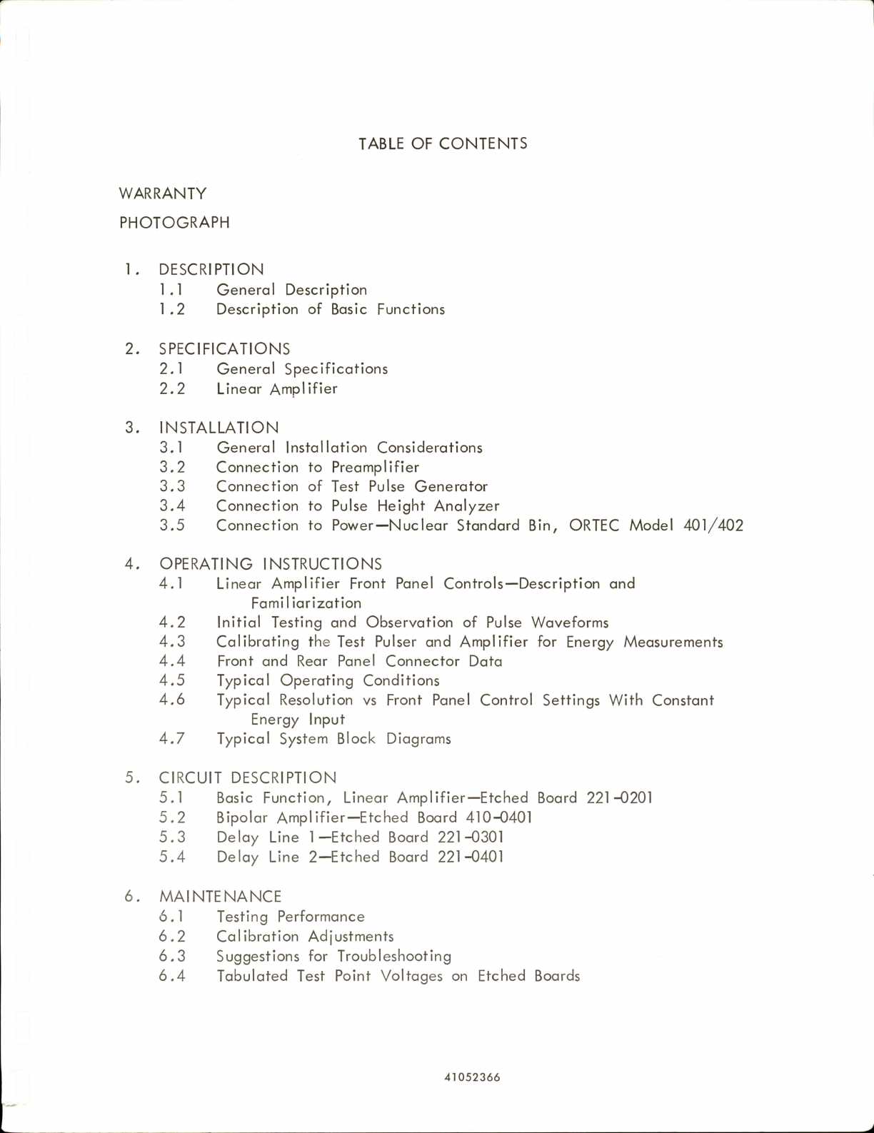
ORTEC 410 User manual

PRECISION
INSTRUMENTATION
FOR
RESEARCH
i
■
'Sx-tifn:
I
Oak
Ridge
Technical
Enterprises
Corporation
OAK
RIDGE,
TENNESSEE
*
I
INSTRUCTION
MANUAL
MODEL
410
LINEAR
AMPLIFIER
l»
is
.m
L

INSTRUCTION
MANUAL
MODEL
410
LINEAR
AMPLIFIER
Serial
No.
Purchaser
_
Date
Issued
OAK
RIDGE
TECHNICAL
ENTERPRISES
CORPORATION
P.O.
BOX
C
OAK
RIDGE,
TENNESSEE
Telephone
(615)
483-8451
TWX
(810)
572-1078
)
Oak
Ridge
Technical
Enterprises
Corporation
1966
Printed
in
U.S.A.
41052366
r

TABLE
OF
CONTENTS
WARRANTY
PHOTOGRAPH
1.
DESCRIPTION
1
.1
General
Description
1
.2
Description
of
Basic
Functions
SPECIFICATIONS
2.1
General
Specifications
2.2
Linear
Amplifier
INSTALLATION
3.1
General
Installation
Considerations
3.2
Connection
to
Preamplifier
3.3
Connection
of
Test
Pulse
Generator
3.4
Connection
to
Pulse
Height
Analyzer
3.5
Connection
to
Power—Nuclear
Standard
Bin,
ORTEC
Model
401/402
4.
OPERATING
INSTRUCTIONS
4.1
Linear
Amplifier
Front
Panel
Controls—Description
and
Familiarization
4.2
Initial
Testing
and
Observation
of
Pulse
Waveforms
4.3
Calibrating
the
Test
Pulser
and
Amplifier
for
Energy
Measurements
4.4
Front
and
Rear
Panel
Connector
Data
4.5
Typical
Operating
Conditions
4.6
Typical
Resolution
vs
Front
Panel
Control
Settings
With
Constant
Energy
Input
4.7
Typical
System
Block
Diagrams
5.
CIRCUIT
DESCRIPTION
5.1
Basic
Function,
Linear
Amplifier—Etched
Board
221-0201
5.2
Bipolar
Amplifier—Etched
Board
410-0401
5.3
Delay
Line
1—Etched
Board
221-0301
5.4
Delay
Line
2—Etched
Board
221-0401
6.
MAINTENANCE
6.1
Testing
Performance
6.2
Calibration
Adjustments
6.3
Suggestions
for
Troubleshooting
6.4
Tabulated
Test
Point
Voltages
on
Etched
Boards
41052366
J

LIST
OF
ILLUSTRATIONS
igure
4-1
.
Measuring
Amplifier
and
Detector
Noise
Resolution
igure
4-2,
Resolution
Spread
versus
External
Input
Capacity
igure
4-3,
Amplifier
and
Detector
Noise
versus
Bias
Voltage
igure
4-4,
Measuring
Resolution
With
a
Pulse
Height
Analyzer
igure
4-5,
High-Resolution
Spectroscopy
System
igure
4-6,
Measuring
Detector
Current-Voltage
Characteristics
igure
4-7,
Detector
Back
Current
versus
Bias
Voltage
igure
4-8,
Neutron
Spectrometer
Using
Sandwich
Detector
igure
4-9,
Gamma
Ray—Charged
Particle
Coincidence
Experiment—Block
Diagram
igure
4-10,
Time-of-Flight
Neutron
Spectrometer—Block
Diagram
igure
4-11
,
Gamma
Ray
Pair
Spectrometer—Block
Diagram
igure
4-12,
Typical
Fast-Slow
Coincidence
System—Block
Diagram
igure
5-1
,
Basic
Feedback
Amplifier
Loop
igure
5-2,
Output
Waveform
of
Bipolar
Amplifier
(RC
pulse
shaping)
igure
6-1
,
Impedance
Transformation
(Minimum-Loss
Pad)
41052366

STANDARD
WARRANTY
FOR
ORTEC
ELECTRONIC
INSTRUMENTS
DAMAGE
IN
TRANSIT
Shipments
should
be
examined
immediately
upon
receipt
for
evidence
of
external
or
con
cealed
damage.
The
carrier
making
delivery
should
be
notified
immediately
of
any
such
damage,
since
the
carrier
is
normally
liable
for
damage
in
shipment.
Packing
materials,
waybills,
and
other
such
documentation
should
be
preserved
in
order
to
establish
claims.
After
such
notification
to
the
carrier,
notify
ORTEC
of
the
circumstances
so
that
we
may
assist
in
damage
claims
and
in
providing
replacement
equipment
when
necessary.
WARRANTY
ORTEC
warrants
its
electronic
products
to
be
free
from
defects
in
workmanship
and
materials,
other
than
vacuum
tubes
and
semiconductors,
for
a
period
of
twelve
months
from
date
of
ship
ment,
provided
that
the
equipment
has
been
used
in
a
proper
manner
and
not
subjected
to
abuse.
Repairs
or
replacement,
at
ORTEC
option,
will
be
made
without
charge
at
the
ORTEC
factory.
Shipping
expense
will
be
to
the
account
of
the
customer
except
in
cases
of
defects
discovered
upon
initial
operation.
Warranties
of
vacuum
tubes
and
semiconductors,
as
made
by
their
manufacturers,
will
be
extended
to
our
customers
only
to
the
extent
of
the
manufacturers'
liability
to
ORTEC.
Specially
selected
vacuum
tubes
or
semiconductors
cannot
be
warranted.
ORTEC
reserves
the
right
to
modify
the
design
of
its
products
without
incurring
responsibility
for
modification
of
previously
manufactured
units.
Since
installation
conditions
are
beyond
our
control,
ORTEC
does
not
assume
any
risks
or
liabilities
associated
with
the
methods
of
installation,
or
installation
results.
QUALITY
CONTROL
Before
being
approved
for
shipment,
each
ORTEC
instrument
must
pass
a
stringent
set
of
quality
control
tests
designed
to
expose
any
flaws
in
materials
or
workmanship.
Permanent
records
of
these
tests
are
maintained
for
use
in
warranty
repair
and
as
a
source
of
statistical
information
for
design
improvements.
REPAIR
SERVICE
ORTEC
instruments
not
in
warranty
may
be
returned
to
the
factory
for
repairs
or
checkout
at
modest
expense
to
the
customer.
Standard
procedure
requires
that
returned
instruments
pass
the
same
quality
control
tests
as
those
used
for
new
production
instruments.
Please
contact
the
factory
for
instructions
before
shipping
equipment.

1-1
MODEL
410
LINEAR
AMPLIFIER
1
.
DESCRIPTION
1
.1
General
DescripHon
The
ORTEC
Model
410
Linear Amplifier
is
a
very
versatile
linear
amplifier
designed
to
optimize
both
energy
and
time
measurement
capa
bilities
from
nuclear
radiation
detectors.
The
instrument
features
high
counting
rote
capabilities,
overload
recovery,
and
the
ultimate
in
resolution
necessary
for
use
with
semiconductor,
gaseous,
and
scintillation
detectors.
The
amplifier
is
packaged
in
the
AEG-recommended
Nuclear
Standard
Module.
The
linear
functions
include
a
Linear
Amplifier
with
a
positive
unipolar
output
signal,
and
a
Bipolar
Amplifier
with
a
bipolar
output.
The
Linear
Amplifier
and
the
Bipolar
Amplifier
both
include
delay
line
and
RC
pulse
shaping.
The
RC
pulse
shaping
features
variable
time
constants
ranging
from
0.1
to
10
microseconds.
The
delay
line
shaped
pulse
is
0.8
micro
second
wide.
The
timing
function
is
performed
when
the
Model
410
is
used
in
conjunc
tion
with
an
ORTEC
Model
407
or
Model
420
Crossover
Pickoff
circuit.
The
resulting
crossover
pickoff
output
features
a
minimum
of
walk
as
a
function
of
pulse
amplitude,
and
also
incorporates
a
variable
delay
time
on
the
output
pulse
to
enable
the
crossover
pickoff
output
to
be
placed
in
time
coincidence
with
other
signals.
The
Model
410
has
complete
provisions,
including
power,
for
operating
an
ORTEC
solid
state
preampl
ifier
such
as
the
Model
108,
109,
or
113.
Al
l
signal
inputs
and
outputs
are
available
on
BNC
connectors
mounted
on
the
front
panel
.
Observation
of
signal
waveforms
with
an
oscil
lo
scope
is
facilitated
with
two
convenient
test
point
jacks
located
on
the
front
panel
.
The
Linear
Amplifier
accepts
either
positive
or
negative
input
signals
from
the
preampl
ifier,
and
features
fast
rise
time,
very
low
equivalent
input
noise,
and
variable
pulse
shaping
time
constants
to
allow
the
energy
and
time
resolution
to
be
optimized
for
a
given
set
of
experi
mental
conditions.
The
input
impedance
of
the Linear
Amplifier
is
125
ohms;
therefore,
it
is
not
necessary
to
terminate
long
125-ohm
(RG-63/U)
cable
runs
at
the
preamplifier,
since
they
are
terminated
at
the
input
to
the
main
amplifier.
The
input
impedance
can
be
shunted
at
the
input
41052366

1-2
BNC
connector
to
obtain
any
impedance
level
less
than
125
ohms,
i.e.,
93
ohms
or
50
ohms.
Output
signal levels
from
the
ORTEC
Models
105,
105XL,
108, 109,
and
1
13
preamplifiers
are
directly
compatible
with
the
Model
410.
The
output
impedance
of
the
unipolar
and
bipolar
output
circuitry
is
ap
proximately
1
ohm,
and
short-circuit
protected;
therefore,
changes
in
gain
cal
ibration
of
multichannel
analyzers
or
other
output
equipment
are
minimized
when
additional
output
equipment
such
as
single
channel
analyzers
and
count
rate
meters
must
be
added
to
the
output
of
the
linear
circuitry
after
initial
gain
calibration.
The
Model
410
is
three
Nuclear
Standard
Module
widths
wide.
The
module
has
no
self-contained
power
supply;
power
is
obtained
from
a
Nuclear
Standard
Bin
and
Power
Supply
such
as
the
ORTEC
Model
401/402.
1
.2
Description
of
Basic
Functions
1
.2.
1
Linear
AmpI
ifier
The
Linear
Ampl
ifier
features
a
very
low
equivalent
input
noise
and
variable
bandwidth
which
greatly
aid
in
optimizing
the
signal-to-noise
ratio
for
a
given
set
of
detector
operating
con
ditions.
The
bandwidth
is
selected
by
front
panel
switches
which
independently
set
the
differentiation
and
integration
time
con
stants.
Two
modes
of
signal
differentiation
are
provided,
delay
line
and
RC.
The
delay
l
ine
differentiator
is
normal
ly
suppl
ied
as
0.8-microsecond
but
may
be
shortened
or
lengthened
if
desired,
The
RC
differentiation
is
variable
from
0.
1
to
10
microseconds
in
a
1-2-5
sequence.
Single
integration
is
provided
from
0.
1
to
10
microseconds
also
in
the
1-2-5
sequence.
If
desired,
the
differentiation
and
integration
networks
can
be
independently
switched
out,
resulting
in
an
ampl
ifier
with
a
flat
frequency
response
from
approximately
670
cps
to
3.5
Mcps.
The
output
from
the
Linear
Amplifier
is
a
positive
unipolar
pulse
of
0
to
10
volts
rated
output
and
12
volts
maximum
output.
1
.2.2
Bipolar
Amplifier
The
Bipolar
Ampl
ifier
l
inearly
converts
the
unipolar
signal
from
the
Linear
Amplifier
to
a
bipolar
pulse.
The
bipolar
pulse
is
selectable
via
front
panel
controls
to
be
either
double
delay
line
or
double
RC
differentiated.
The
second
delay
line
differentiator
is
normal
ly
suppl
ied
to
match
the
delay
line
differentiating
time
of
the
main
amplifier.
The
second
RC
differentiator
is
selectable
41052366

1-3
over
the
same
range
and
in
the
same
steps
as
the
first
RC
dif
ferentiator
in
the
main
amplifier.
This
doubly
differentiated
signal
results
in
equal
area
above
and
below
the
baseline
of
the
bipolar
pulse,
and
therefore
permits
a
much
higher
counting
rate
with
less
baseline
distortion
than
in
the
case
of
a
single
dif
ferentiated
unipolar
pulse.
The
output
of
the
Bipolar
Amplifier
is
0
to
±
10
volts
rated
output
and
12
volts
maximum
output.
41052366

2-1
2.
SPECIFICATIONS
2,
1
General
Specifications
2.1.1
The
Model
410
is
intended
for
use
with
a
Nuclear
Standard
Bin
such
as
the
ORTEC
Model
401/402.
Seven
watts
of
power
are
required
for
the
operation
of
the
Model
410
in
the
quiescent
condition.
The
ORTEC
Model
401/402
can
be
operated
on
either
1
15
or
220
volts
ac,
50—60
ops;
if
it
is
used
with
220
volts
ac,
the
manual
for
the
Model
401/402
must
be
referred
to
in
order
to
ensure
that
correct
connections
have
been
made
before
operation
on
220
volts
ac
is
attempted.
The
instrument
is
supplied
from
the
factory
wired
for
115
volts
ac
operation.
The
power
input
connector
to
the
Model
401/402
is
a
NEMA
standard
3
-wire
grounding
type.
Preompl
ifier
power
of±
1
2V
and
±
24V
is
available
on
the
Model
410
rear
panel
connector,
PG5,
an
Amphenol
17-10090.
Al
l
signal
inputs
and
outputs
are
on
BNC
connectors
which
are
mounted
on
the
front
panel
.
2.1.2
The
instrument
is
intended
for
rack
mounting
in
an
ORTEC
Model
401/402
Nuclear
Standard
Bin,
but
the
Nuclear
Standard
Bin
is
suitably
packaged
for
cabinet
instal
lation
if
desired.
The
weight
of
the
Model
410
is
4.3
pounds
and
its
outside
dimensions
are
ap
proximately
8.75
inches
high
by
4.05
inches
wide
by
9.75
inches
deep.
2.2
Linear
Amplifier
Input
Polarity
Maximum
Input
Signal
Input
Impedance
Either
positive
or
negative
With
the
INPUT
ATTENUATOR
set
on
1,
on
input
up
to
plus
or
minus
2.5
volts
wil
l
not
saturate
the
amplifier.
Larger
inputs
can
be
attenuated
to
the
2.5V
level
with
the
input
attenuator.
Constant
125
ohms;
con
be
shunted
on
INPUT
BNC
connector
with
pure
resistance
to
achieve
93
ohms
or
50
ohms
if
desired.
Total
Gain
RC
shaping
mode
0.35
to
480
Delay
Line
shaping
mode
0.75
to
1300
41052366

2-2
Gain
Adjustment
Actual
gain
control
led
by
three
gain
controls—
A.
INPUT
ATTENUATOR:
Attenuation
factors
1,
2,
5,
10,
20,
50
B.
FINE
GAIN:
1
.0
to
3.0
C.
COARSE
GAIN:
XI,
X3,
X9
Pulse
Shaping
Modes
Two
basic
pulse
shaping
modes
pro
vided
_
A.
Classical
RC
pulse
shaping
B.
Delay
Line
pulse
shaping
The
mode
desired
is
selectable
via
front
panel
switch.
RC
time
constants,
i.e.,
r
=
l/e,
are
selectable
from
0.1,
0.2,
0.5,
1,
2,
5,
and
lOpsec.
The
time
constants
are
accurate
to
±2%
of
indicated
value.
The
delay
l
ine
normal
ly
supplied
provides
a
ful
l
width
at
half
maximum
(fwhm)
output
pulse
of
0.8
p
sec
.
Other
pulse
widths
are
supplied
on
special
request.
The
pulse
shaping
net
works
can
be
switched
to
the
OUT
position,
resulting
in
an
ampl
ifier
with
a
flat
bandpass
from
approxi
mately
760
ops
to
3.5
Mcps.
Amplifier
Rise
Time
Unipolar
Output—80
nsec
Bipolar
Output—100
nsec
Maximum
Amplifier
Bandpass
Within
3
db
from
700
cycles
to
4.3
megacycles
Output
Unipolar—0
to
lOV
positive,
12V
maximum
Bipolar—0
to
lOV
positive
and
negative,
i.e.,
bipolar;
12V
maximum
output
41052366

2-3
Output
Impedance,
Amplifier
Noise
.
,
Overload
Performance
Approximately
1
ohm,
short-circuit
protected
Equivalent
noise
at
unipolar
output
when
referred
to
the
Input
Is
less
than
7
pV
rms
with
maximum
am
plifier
gain
and
1st
DIFFERENTIA
TION
and
INTEGRATION
set
on
1
p
sec
pulse
shaping.
Amplifier
recovers
from
a
300X
over
load
to
less
than
2%
of
rated
output
voltage
within
4psec
when
used
with
maximum
gain
In
the
double
delay
line
shaping
mode.
The
over
load
factor
Is
approximately
lOOX
when
used
with
RC
pulse
shaping.
Temperature
Stability
Gain
shift
Is
less
than
0.015%
per°C.
Linearity
The
nonllnearlty
Is
less
than
0.2%
from
200
mV
to
8V
and
less
than
0.3%
to
lOV.
Counting
Rate
The
shift
In
gain
as
a
function
of
counting
rate
Is
less
than
0.2%
for
50,000
cts/sec
from
a
Cs^^^
source
with
a
60
keV
threshold
on
the
counting.
Operating
Temperature
Power
Required
0
to
50°C.
Model
410
power
supplied
from
ORTEC
Model
401/402
Power
Supply
DC
input
voltage
Quiescent
current
Current
with
50,000
pulses
per
second,
each
pulse
8V
into
100
ohms
+24V
146
mA
150
mA
-24V
78
mA
78
mA
+
12V
—
5.6
mA
—5.5
mA
-12V
18
mA
22.5
mA
41052366

3--
3.
INSTALLATION
3.1
General
Insl-al
lation
Considerations
The
Model
410
used
In
conjunction
with
a
Model
401/402
Bin
and
Power
Supply
Is
Intended
for
rack
mounting,
and
therefore
If
Is
necessary
to
ensure
that
vacuum
tube
equipment
operating
In
the
same
rack
with
the
Model
410
has
sufficient
cool
ing
olr
circulating
to
prevent
any
local
ized
heating
of
the
al
l-transistor
circuitry
used
throughout
the
Model
410.
The
temperature
of
equipment
mounted
In
racks
can
easily
exceed
120"
F
(50
"C)
unless
pre
cautions
are
taken.
3.2
Connection
to
Preampl
ifier
The
preampl
ifier
output
signal
can
be
connected
to
the
Model
410
via
BNC
connector
PGl
.
The
Input
Impedance
seen
at
PGl
Is
125
ohms
and
Is
dc
coupled
to
ground;
therefore,
the
output
of
the
preampl
ifier
musf
be
either
ac
coupled
to
have
zero
dc
potential
on
the
output
connector.
With
the
flexibility
of
variable
pulse
shaping
time
constants
available
In
the
Model
410,
the
differentiation,
or
fal
l
time,
of
the
preampi
Ifler
output
signal
must
be
taken
Into
consideration
when
setting
up
a
l
inear
system.
The
nominal
fal
l
time
back
to
the
basel
ine
of
ORTEC
preampl
ifiers
Is
ap
proximately
50
microseconds.
If
It
Is
desired
to
use
the
10-mIcrosecond
Integration
and
differentiation
time
constants
of
fhe
Model
410,
It
can
be
seen
that
the
50-mIcrosecond
fal
l
flme
of
the
preampl
ifier
actual
ly
con
stitutes
an
additional
differentiation
time
constant.
This
can
result
In
triple
differentiation
of
the
signal
at
the
bipolar
output.
Triple
differentia
tion
wil
l
cause
the
Input
signal
to
cross
the
basel
ine
twice
and
result
In
a
nonnegl
Iglble
positive
overshoot
after
the
Initial
normal
positive
and
negative
bipolar
signal
.
To
avoid
this
condition
the
fal
l
time
of
the
pre
ampl
ifier
must
be
lengthened,
preferably
fo
a
minimum
of
25
times
as
long
as
the
pulse
shaping
time
constant.
Detailed
Instructions
for
lengthening
the
fal
l
time
In
ORTEC
preampl
ifiers
wil
l
be
found
In
the
Instruction
manual
for
fhe
respective
preamplifier.
Preampl
ifier
power
of
±
12V
and
±24V
are
available
on
the
preamp
power
connector,
PG5.
When
using
the
Model
410
with
a
remotely
located
preamplifier
(I.e.,
pre
ampi
Ifler-to-ampI
Ifler
connecflon
through
25
feet
or
more
of
coaxial
cable),
care
must
be
taken
to
ensure
that
the
characteristic
Impedance
of
the
trans
mission
l
ine
from
the
preamplifier
oufpuf
to
the
Model
410
Input
Is
matched.
Since
the
Input
Impedance
of
fhe
Model
410
Is
125
ohms,
receiving
end
ter
mination
wil
l
normal
ly
be
preferred;
I.e.,
the
transmission
line
should
be
terminated
at
the
Input
of
fhe
Model
410.
For
maximum
performance
from
41052366

3-2
the
Model
410
and
the
associated
preampl
ifier,
high
qual
ity
coaxial
cable
such
as
RG-63/U
must
be
used
for
the
connections
from
the
preamplifier
output
to
the
Linear
Ampl
ifier
input.
In
the
event
RG-63/U
or
other
125-ohm
coaxial
cable
is
unavailable,
a
minimum-loss
impedance
trans
formation
can
be
inserted
in
series
between
the
transmission
l
ine
from
the
preampl
ifier
and
the
Linear
Ampl
ifier
input
at
PGl
.
Recommended
values
of
resistors
for
various
impedance
transformations
are
given
in
Section
6.2.3.
3.3
Connection
of
Test
Pulse
Generator
3.3.
1
Connection
of
Pulse
Generator
to
Model
410
Through
a
PreampI
ifier
The
satisfactory
connection
of
a
test
pulse
generator
such
as
the
ORTEC
Model
419
or
equivalent
depends
primari
ly
on
two
considerations:
(1)
the
preamplifier
must
be
properly
connected
to
the
Model
410
as
discussed
in
Section
3.2,
and
(2)
the
proper
input
signal
simulation
must
be
applied
to
the
preampl
ifier.
To
ensure
proper
input
signal
simulation,
refer
to
the
instruction
manual
for
the
particular
preampl
ifier
being
used.
3.3.2
Direct
Connection
of
Pulse
Generator
to
Model
410
The
Model
410
input,
BNC
connector
PGl,
has
125-ohm
input
impedance
and
feeds
directly
into
the
voltage-sensitive
Linear
Ampl
ifier
circuit.
PGl
is
dc
coupled
to
ground,
and
any
test
pulse
generator
such
as
the
ORTEC
Model
419
with
a
fast
rise
time
and
long
(greater
than
100-microsecond)
exponential
decay
can
be
used
to
test
the
Model
410
l
inear
ampl
ifying
functions.
The
rise
time
of
the
input
signal
should
be
greater
than
35
nsec
for
best
performance
of
the
Model
410.
3.4
Connection
to
Pulse
Height
Analyser
A
choice
of
output
signals
suitable
for
driving
pulse
height
analyzers
is
available
from
the
Model
410.
Prompt
unipolar
and
bipolar
outputs
are
available
at
PG2
and
PG3,
respectively.
It
is
strongly
recommended
that
the
signal
selected
to
be
fed
to
the
input
of
the
pulse
height
analyzer
be
passed
through
a
pulse
stretcher
similar
to
the
ORTEC
Model
41
1
if
the
ful
l
width
at
half
maximum
(fwhm)
is
less
than
0.8
microsecond.
The
pulse
stretcher
wil
l
stretch
the
peak
ampl
itude
of
the
signal
to
a
minimum
of
1
.5
microseconds
and
thereby
reduce
the
band
width
requirements
of
the
analog-to-digital
(ADC)
circuitry
of
the
multi
channel
analyzer.
The
stretched
pulse
results
in
reduced
integral
non-
linearity
of
the
pulse
height
analyzer.
41052366

3-3
The
rated
Iinear
output
voltage
of
the
Model
410
is
0
to
10
vol
ts;
therefore,
the
multichannel
analog-to-digital
converter
(ADC)
should
be
adjusted
to
utilize
this
voltage
range.
It
is
important
to
present
the
signal
to
the
ADC
of
the
analyzer
without
introducing
any
additional
short
time
constant
pulse
shaping
in
the
transition
from
the
Model
410
output
to
the
ADC.
If
addi
tional
pulse
shaping
(i.e.,
clipping)
is
done,
it
wil
l
usual
ly
be
at
the
ex
pense
of
reduced
resolution
of
the
l
inear
system.
3.5
Connection
to
Power—Nuclear
Standard
Bin,
ORTEC
Model
401/402
The
Model
410
contains
no
internal
power
supply
and
therefore
must
obtain
power
from
a
Nuclear
Standard
Bin
and
Power
Supply
such
as
the
ORTEC
Model
401/402.
It
is
recommended
that
the
bin
power
supply
be
turned
off
when
inserting
or
removing
modules.
The
ORTEC
400
Series
is
designed
so
that
it
is
not
possible
to
overload
the
bin
power
supply
with
a
ful
l
com
plement
of
modules
in
the
Bin;
however,
this
may
not
be
true
when
the
Bin
contains
modules
other
than
those
of
ORTEC
design,
and
in
this
case,
the
power
supply
voltages
should
be
checked
after
insertion
of
the
modules.
The
ORTEC
Model
401/402
h
as
test
points
on
the
power
supply
control
panel
to
monitor
the
dc
voltages.
When
using
the
Model
410
outside
the
Model
401/402
Bin
and
Power
Supply,
be
sure
that
the
jumper
cable
used
properly
accounts
for
the
power
supply
grounding
circuits
provided
in
the
recommended
AEC
standards
of
TID-20893.
Both
clean
and
dirty
ground
connections
are
provided
to
ensure
proper
refer
ence
voltage
feedback
into
the
power
supply,
and
these
must
be
preserved
in
remote
cable
instal
lations.
Care
must
also
be
exercised
to
avoid
ground
loops
when
the
module
is
not
physical
ly
in
the
bin.
41052366

4-1
OPERATING
INSTRUCTIONS
4.1
Linear
Ampl
ifier
Front
Panel
Controls—Description
and
Fami
I
iarization
INPUT
POLARITY—Normal
ly
set
to
the
polarity
of
the
input
pulse
at
PGl
.
This
results
In
a
unipolar
positive
output
pulse
at
PG2.
INPUT
ATTENUATOR—A
passive
pi
attenuator
inserted
between
the
input
connector
PGl
and
the
Linear
Ampl
ifier
circuit.
The
attenuation
ratio
is
variable
from
1
to
50
in
the
1-2-5
sequence.
The
input
and
out
put
impedance
of
the
attenuator
remains
constant
at
125
ohms
over
this
range.
FINE
GAIN—Fine
gain
control
of
the
Linear
Ampl
ifier
is
provided
over
a
range
of
1
to
3.
COARSE
GAIN—The
gain
of
the
Linear
Ampl
ifier
can
be
changed
by
a
factor
of
3
by
dial
ing
the
COARSE
GAIN
switch
from
1
to
3
or
to
9.
This
gain
control
is
a
passive
attenuation
network
within
the
circuitry
of
the
Linear
AmpI
ifier.
INTEGRATION—The
integration
time
constant
of
the
Linear
Ampl
ifier
is
selected
with
this
control
.
Integration
times
are
selectable
over
the
range
of
0.
1
to
10
microseconds
in
the
1-2-5
sequence
.
The
integration
time
constant
can
be
switched
to
OUT,
resulting
in
a
maximum
upper
frequency
response,
f„
,
of
approximately
3.5
Mc
(3-db
point).
The
OUT
position
wil
l
be
used
if
integration
of
the
pulse
shape
is
being
performed
in
the
preamplifier.
Ist
DIFFERENTIATION—The
differentiation
(cl
ipping)
time
constant
of
the
Linear
Ampl
ifier
is
selectable
via
the
outer
concentric
knob
of
the
DIF
FERENTIATION
control
.
Differentiation
time
constants
are
variable
from
0.1
to
10
microseconds
in
the
RC
shaping
mode,
and
are
normal
ly
fixed
at
0.8
microsecond
for
the
delay
l
ine
(DL)
mode.
In
addition
to
the
RC
and
DL
modes
of
shaping,
an
OUT
position
is
provided
that
decreases
the
lower
frequency
response,
f^
,
of
the
ampl
ifier
to
approximately
670
cps.
The
OUT
position
wil
l
be
used
if
al
l
differentiation
is
being
accomplished
in
the
preampiifier.
2nd
DIFFERENTIATION
—The
unipolar
output
of
the
Linear
Ampl
ifier
Is
passed
through
a
second
differentiation
network
to
produce
a
bipolar
signal
.
The
differentiation
time
constant
is
control
led
by
the
inner
con
centric
knob
of
the
DIFFERENTIATION
control
.
While
this
control
is
completely
independent
of
the
first
(1st)
DIFFERENTIATION
control,
the
range
of
time
constants
is
exactly
the
same,
i.e.,
0.1
to
10
microseconds
41052366

4-2
in
the
RC
mode
and
normal
ly
0.8
microsecond
in
the
Delay
Line
mode.
An
OUT
position
is
also
provided
on
the
second
(2nd)
DIFFERENTIATION
sv^itch.
4.2
Initial
Testing
and
Observation
of
Pulse
Waveforms
Refer
to
Section
6.1
for
information
on
testing
performance
and
observing
waveforms
at
front
panel
test
points.
4.3
Calibrating
the
Test
Pulser
and
Amplifier
for
Energy
Measurements
4.3.
1
Calibration
of
Test
Pulser
The
ORTEC
Model
419
mercury
pulser,
or
equivalent,
may
easily
be
cal
ibrated
so
that
the
maximum
pulse
height
dial
reading
(1000
divisions)
is
equivalent
to
a
10-MeV
loss
in
a
sil
icon
radiation
detector.
The
procedure
is
as
fol
lows:
(1)
Connect
the
detector
to
be
used
to
the
spectrometer
system,
i.e.,
preomp,
main
amplifier,
and
bias
amplifier.
(2)
Al
lovy'particles
from
a
source
of
known
energy
(a-particles,
for
example)
to
fal
l
on
the
detector.
(3)
Adjust
the
amplifier
gains
and
the
bias
level
of
the
biased
amplifier
to
give
a
suitable
output
pulse.
(4)
Set
the
pulser
PULSE
HEIGHT
potentiometer
at
the
energy
of
the
a-particles
striking
the
detector
(e.g.,
for
a
5.1-
MeV
Q-partlcle,
set
the
dial
at
510
divisions).
(5)
Turn
on
the
Pulser;
use
the
NORMALIZE
potentiometer
and
attenuators
to
set
the
output
due
to
the
pulser
to
the
same
pulse
height
as
the
pulse
obtained
in
(3)
above.
(6)
The
pulser
Is
now
calibrated;
the
dial
reads
in
MeV
if
the
number
of
dial
divisions
is
divided
by
100.
4.3.2
Amplifier
Noise
and
Resolution
Measurements
As
shown
in
Figure
4-1,
the
preamplifier,
amplifier,
pulse
generator,
oscil
loscope,
and
a
wide-bond
rms
voltmeter
such
as
the
Hewlett-Packard
400D
are
required
for
this
measurement.
Connect
a
suitable
capacitor
to
the
input
to
simulate
the
detector
capacitance
desired.
To
obtain
the
resolution
spread
due
to
am
plifier
noise:
41052366

4-3
4=
(DETECTOR
OR
CAPACITOR)
ORTEC
MODEL
109
PRE
AMPLIFl
ER
ORTEC
MODEL
410
LINEAR
AMP
ORTEC
MODEL
419
PULSE
GENERATOR
OSCILLOSCOPE
RMS
VOLTMETER
Figure
4-1.
Measuring
Amplifier
and
Detector
Noise
Resolution
ODEL
105
PREAMP
0DEL4I0
LINEAR
SINGLE
RC
DIFF.
S
M
LIFIER
M
AMP
INTEG.
20
15
>
a>
iio
$
0
100
200
EXTERNAL
INPUT
CAPACITY
(pF)
300
Figure
4-2.
Resolution
Spread
versus
External
Input
Capacity
41052366

4-4
(1)
Measure
the
rms
noise
voltage
at
PG2,
the
Linear
Amp!ifier
output.
(2)
Turn
on
the
Model
419
mercury
relay
pulse
generator
and
adjust
the
Linear
Ampl
ifier
output
to
any
convenient
read
able
voltage,
Eq
,
at
PG2
as
determined
by
the
oscil
lo
scope
.
(3)
The
ful
l
width
at
half
maximum
(fwhm)
resolution
spread
due
to
ampl
ifier
noise
is
then
N
(fwhm)
=
2.660
E
E
I
rms
dial
where
E^j^|
is
the
pulser
dial
reading
in
MeV
and
the
factor
2.660
is
the
correction
factor
for
rms
to
fwhm
(2.35)
and
noise
to
rms
meter
correction
(1
.13)
for
average-
indicating
voltmeters
such
as
the
Hewlett-Packard
400D.
The
resolution
spread
wil
l
depend
upon
the
total
input
capaci
tance,
since
the
capacitance
degrades
the
signal-to-noise
ratio
much
faster
than
the
noise.
A
typical
resolution
spread
versus
external
input
capacitance
for
the
Model
105—Model
410
system
in
RC
mode
is
shown
in
Figure
4-2.
4.3,3
Detector
Noise
Resolution
Measurements
The
same
measurement
described
in
Section
4.3.2
can
be
made
with
a
biased
detector
instead
of
the
external
capacitor
used
to
simulate
the
detector
capacitance.
The
resolution
spread
wil
l
be
larger
because
the
detector
contributes
both
noise
and
capa
citance
to
the
input.
The
detector
noise
resolution
spread
can
be
isolated
from
the
amplifier
noise
spread
if
the
detector
capacity
is
known,
since
N
,
+
N
^
=
N,
,
det
amp
total
Where
is
the
total
resolution
spread
and
Nq^p
is
the
amplifier
resolution
spread
with
the
detector
replaced
by
its
equivalent
capacitance.
The
detector
noise
tends
to
increase
with
bias
voltage,
but
the
detector
capacitance
decreases,
thus
reducing
the
resolution
spread.
The
overal
l
resolution
spread
wil
l
depend
upon
which
41052366

4-5
(/)
!3
O
>
z
HI
(✓>
o
z
«/)
A-ORTEC
SBDJ007-400
No.
B
30
B-ORTEC
SBEE050-60
No.2-360
C-
ORTEC
SBEE100-60
No.
494
D-ORTEG
SBDJ200-60
No.
089
E-
ORTEC
SBQN450-60
No.653
50
75
BIAS
VOLTAGE
100
125
Figure
4-3.
Amplifier
and
Detector
Noise
versus
Bios
Voltage
ORTEC
MODEL
419
PULSE
GENERATOR
ORTEC
109
PREAMP
ORTEC
MODEL
410
LINEAR
AMPLIFIER
ORTEC
MODEL
408
BIASED
AMP
T
(
DETECTOR
OR
CAPACITOR)
ORTEC
MODEL
411
PULSE
STRETCHER
MULTICHANNEL
PULSE
HEIGHT
ANALYZER
Figure
4-4.
Measuring
Resolution
With
a
Pulse
Height
Analyzer
41052366

4-6
effect
is
dominant.
Figure
4-3
shows
curves
of
typical
total
noise
resolution
spread
versus
bias
voltage,
using
the
data
from
several
ORTEC
silicon
semiconductor
radiation
detectors.
4.3.4
Amplifier
Noise
and
Resolution
Measurements
Using
a
Pulse
Height
Analyzer
Probably
the
most
convenient
method
of
making
resolution
measurements
Is
with
a
pulse
height
analyzer
as
shown
by
the
setup
Il
lustrated
In
Figure
4-4.
The
amplifier
noise
resolution
spread
can
be
measured
directly
with
a
pulse
height
analyzer
and
the
mercury
pulser
as
fol
lows:
(1)
Select
the
energy
of
Interest
with
an
ORTEC
Model
419
Pulse
Generator,
and
set
the
Linear
Amplifier
and
Biased
Amplifier
GAIN
and
BIAS
LEVEL
controls
so
that
the
energy
Is
In
a
convenient
channel
of
the
analyzer.
(2)
Calibrate
the
analyzer
In
keV
per
channel,
using
the
pulser
(full
scale
on
the
pulser
dial
Is
10
MeV
when
calibrated
as
described
In
section
4.3.1).
(3)
The
amplifier
noise
resolution
spread
can
then
be
obtained
by
measuring
the
full
width
at
half
maximum
(fwhm)
of
the
pulser
spectrum.
The
detector
noise
resolution
spread
for
a
given
detector
bias
can
be
determined
In
the
same
manner
by
connecting
a
detector
to
the
preamplifier
Input.
The
amplifier
noise
resolution
spread
must
be
subtracted
as
described
In
section
4.3.3.
The
detector
noise
will
vary
with
detector
size,
bias
conditions,
and
possibly
with
ambient
conditions.
4.3.5
Alpha-Particle
Resolution
Alpha-particle
resolution
may
be
determined
by
a
setup
such
as
that
shown
In
Figure
4-5.
The
source
must
be
sufficiently
"thin"
so
that
the
source
Itself
does
not
affect
the
resolution.
High-
resolution
a-measurements
MUST
be
made
In
a
vacuum
of
0.05
mm
mercury,
or
less.
The
alpha-particle
resolution
Is
obtained
In
the
following
manner:
(1)
Use
Preamplifier,
Linear
Amplifier,
Biased
Amplifier
GAIN
and
BIAS
LEVEL
control
settings
which
wil
l
place
the
a-
41052366
Table of contents
Other ORTEC Amplifier manuals