ORTEC 460 Service manual

Model 460
Delay Line Amplifier
Operating and Service Manual
Printed in U.S.A. ORTEC®Part No. 733320 1202
Manual Revision C

Advanced Measurement Technology, Inc.
a/k/a/ ORTEC®, a subsidiary of AMETEK®, Inc.
WARRANTY
ORTEC* warrants that the items will be delivered free from defects in material or workmanship. ORTEC makes
no other warranties, express or implied, and specifically NO WARRANTY OF MERCHANTABILITY OR
FITNESS FOR A PARTICULAR PURPOSE.
ORTEC’s exclusive liability is limited to repairing or replacing at ORTEC’s option, items found by ORTEC to
be defective in workmanship or materials within one year from the date of delivery. ORTEC’s liability on any
claim of any kind, including negligence, loss, or damages arising out of, connected with, or from the performance
or breach thereof, or from the manufacture, sale, delivery, resale, repair, or use of any item or services covered
by this agreement or purchase order, shall in no case exceed the price allocable to the item or service furnished
or any part thereof that gives rise to the claim. In the event ORTEC fails to manufacture or deliver items called
for in this agreement orpurchaseorder, ORTEC’s exclusiveliabilityandbuyer’s exclusive remedy shallbe release
of the buyer from the obligation to pay the purchase price. In no event shall ORTEC be liable for special or
consequential damages. Quality Control
Before being approved for shipment, each ORTEC instrument must pass a stringent set of quality control tests
designed to expose any flaws in materials or workmanship. Permanent records of these tests are maintained for
use in warranty repair and as a source of statistical information for design improvements.
Repair Service
If it becomes necessary to return this instrument for repair, it is essential that Customer Services be contacted in
advance of its return so that a Return Authorization Number can be assigned to the unit. Also, ORTEC must be
informed, either in writing, by telephone [(865) 482-4411] or by facsimile transmission[(865) 483-2133], of the
nature of the fault of the instrument being returned and of the model, serial, and revision ("Rev" on rear panel)
numbers. Failure to do so may cause unnecessary delays in getting the unit repaired. The ORTEC standard
procedure requires that instruments returned for repair pass the same quality control tests that are used for
new-production instruments. Instruments that are returned should be packed so that they will withstand normal
transit handling and must be shipped PREPAID via Air Parcel Post or United Parcel Service to the designated
ORTEC repair center. The address label and the package should include the Return Authorization Number
assigned. Instruments being returned that are damaged in transit due to inadequate packing will be repaired at the
sender's expense, and it will be the sender's responsibility to make claim with the shipper. Instruments not in
warranty should follow the same procedure and ORTEC will provide a quotation.
Damage in Transit
Shipments should be examined immediately upon receipt for evidenceof external or concealeddamage. Thecarrier
making deliveryshouldbenotifiedimmediately of any suchdamage, sincethecarrier isnormally liablefor damage
in shipment. Packing materials, waybills, and other such documentation should be preserved in order to establish
claims. After such notification to the carrier, please notify ORTEC of the circumstances so that assistance can be
provided in making damage claims and in providing replacement equipment, if necessary.
Copyright © 2002, Advanced Measurement Technology, Inc. All rights reserved.
*ORTEC®is a registered trademark of Advanced Measurement Technology, Inc. All other trademarks used
herein are the property of their respective owners.

iii
CONTENTS
WARRANTY ....................................................................... ii
SAFETY INSTRUCTIONS AND SYMBOLS ............................................... iv
SAFETY WARNINGS AND CLEANING INSTRUCTIONS ..................................... v
1. DESCRIPTION................................................................... 1
1.1. GENERAL ................................................................ 1
1.2. DUALOUTPUTS ........................................................... 1
1.3. POLE-ZEROCANCELLATION................................................. 1
2. SPECIFICATIONS ................................................................ 2
3. INSTALLATION .................................................................. 3
3.1. GENERAL ................................................................ 3
3.2. CONNECTIONTOPREAMPLIFIER............................................. 3
3.3. CONNECTIONOFTESTPULSEGENERATOR ................................... 4
3.4. CONNECTIONTOPOWER................................................... 4
3.5. SHAPINGCONSIDERATIONS................................................. 4
3.6. SELECTION OF PROMPT OR DELAYED OUTPUT ................................ 5
3.7. OUTPUTCONNECTIONSANDTERMINATINGCONSIDERATIONS ................... 5
4. OPERATING INSTRUCTIONS ....................................................... 5
4.1. INITIAL TESTING AND OBSERVATION OF PULSE WAVEFORMS .................... 5
4.2. FRONTPANELCONTROLS .................................................. 6
4.3. FRONTPANELCONNECTORS(AllTypeBNC) ................................... 6
4.4. REARPANELCONNECTORS................................................. 6
4.5. OPERATION WITH SEMICONDUCTOR DETECTORS .............................. 7
4.6. OPERATION IN NEUTRON-GAMMA DISCRIMINATION SYSTEM WITH STILBENE AND
LIQUIDSCINTILLATORS .................................................... 9
4.7. NEUTRON-GAMMA-RAYDISCRIMINATIONINPROPORTIONALCOUNTERS.......... 12
4.8. OTHEREXPERIMENTS..................................................... 13
4.9. REFERENCES............................................................ 15
5. CIRCUIT DESCRIPTION .......................................................... 16
6. MAINTENANCE................................................................. 18
6.1. TESTEQUIPMENTREQUIRED............................................... 18
6.2. PULSERMODIFICATIONSFOROVERLOADTESTS ............................. 18
6.3. PULSERTEST............................................................ 18
6.4. TROUBLESHOOTING ...................................................... 20
6.5. TABULATEDTESTPOINTVOLTAGESONETCHEDBOARD ....................... 21
6.6. FACTORY REPAIR ........................................................ 21

iv
SAFETY INSTRUCTIONS AND SYMBOLS
This manual contains up to three levels of safety instructions that must be observed in order to avoid
personal injury and/or damage to equipment or other property. These are:
DANGER Indicates a hazard that could result in death or serious bodily harm if the safety instruction
is not observed.
WARNING Indicates a hazard that could result in bodily harm if the safety instruction is not observed.
CAUTION Indicates a hazard that could result in property damage if the safety instruction is not
observed.
Please read all safety instructions carefully and make sure you understand them fully before attempting to
use this product.
In addition, the following symbol may appear on the product:
ATTENTION–Refer to Manual
DANGER–High Voltage
Please read all safety instructions carefully and make sure you understand them fully before attempting to
use this product.

v
DANGER Opening the cover of this instrument is likely to expose dangerous voltages. Disconnect the
instrument from all voltage sources while it is being opened.
WARNING Using this instrument in a manner not specified by the manufacturer may impair the
protection provided by the instrument.
CAUTION To prevent moisture inside of the instrument during external cleaning, use only enough liquid
to dampen the cloth or applicator.
SAFETY WARNINGS AND CLEANING INSTRUCTIONS
Cleaning Instructions
To clean the instrument exterior:
!
Unplug the instrument from the ac power supply.
!
Remove loose dust on the outside of the instrument with a lint-free cloth.
!
Remove remaining dirt with a lint-free cloth dampened in a general-purpose detergent and water
solution. Do not use abrasive cleaners.
!
Allow the instrument to dry completely before reconnecting it to the power source.

vi

1
ORTEC MODEL 460
DELAY LINE AMPLIFIER
1. DESCRIPTION
1.1. GENERAL
The ORTEC 460 Delay Line Amplifier is a nuclear
pulse amplifier that provides delay-line shaping for
all output pulses. It accepts input pulses of either
polarity from the preamplifier and expands their
amplitude by an adjusted gain factor within the
range from 3 through 1000. An integrating time
constant can be selected to shape the rise of the
input pulse as desired. Pole-zero cancellation is
adjustable to match the characteristic of the
preamplifier output.
1.2. DUAL OUTPUTS
Two output pulses are furnished for each input
pulse. One is positive unipolar and is single-delay-
line shaped; it can be furnished as either a prompt
or delayed output pulse. The other is bipolar with
positive polarity leading and is double-delay-line
shaped. Both of these output pulse shapes are
available through front panel connectors with an
output impedance of 1
S
and through rear panel
connectors with an output impedance of 93
S
.
The main use for the unipolar output pulses is for
energy measurements. For this application the 460
provides high counting rate capabilities, excellent
overload recovery, and dc adjustment of the output
baseline. The unipolar output is preferred for both
single-channel and multichannel analysis because
of its low noise characteristic.
The main use for the bipolar output pulses is for
timing measurements using baseline crossover as
the timing indication. Double-delay-line shaping
provides a precision time at the baseline crossover
point that is independent of the pulse amplitude.
1.3. POLE-ZERO CANCELLATION
Pole-zero cancellation is a method for eliminating
pulse undershoot after the first differentiating
network. The technique employed is described by
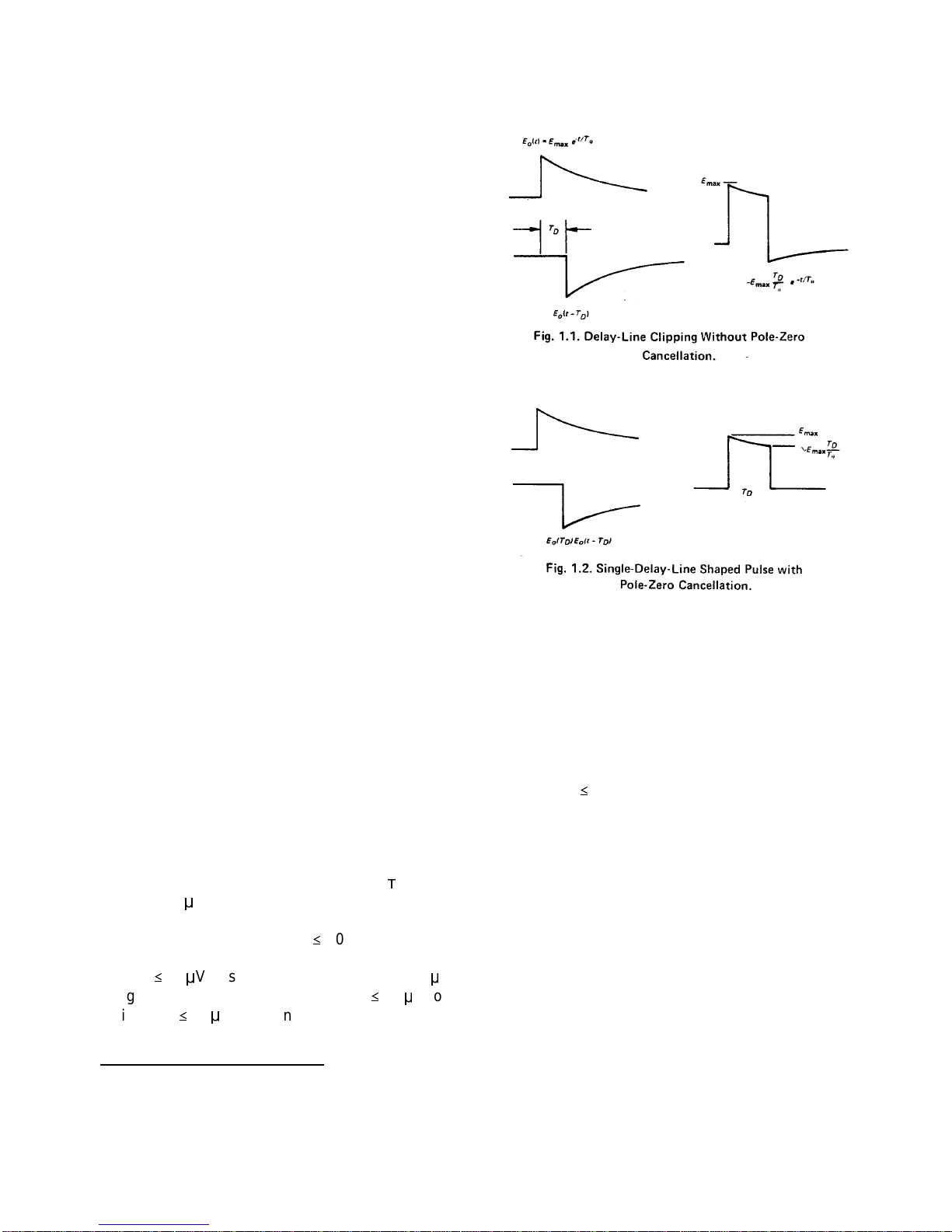
referring to the waveforms and equations shown in
Figs. 1.1 and 1.2. In an amplifier not using pole-
zero cancellation, the exponential tail on the
preamplifier output signal (usually 50 to 500
:
s)
causes an undershoot whose peak amplitude is
roughly
undershoot amplitude =
differentiated pulse amplitude
differentiation time
preamplifier pulse decay time
For a 1-
:
s differentiation on time and a 50-
:
s
preamplifier pulse decay time, the maximum
undershoot is 2% and decays with a 50-
:
s time
constant. Under overload conditions, this
undershoot is often sufficiently large to saturate the
amplifier during a considerable portion of the
undershoot, causing excessive dead time. This
effectcanbereducedbyincreasingthepreamplifier
pulse decay time (which generally reduces the
counting rate capabilities of the preamplifier) or
compensatingfortheundershootbyusingpole-zero
cancellation.
In single-delay-line shaping, differentiation is
accomplished by subtracting a delayed replica of
the signal as shown in Fig. 1.1. The droop in the
input signal during the delay time makes this
subtraction imperfect, and a long under- shoot is
produced. A pole-zero cancellation eliminates this
undershoot by adjusting the amplitude of the
delayed signal as shown in Fig. 1.2.
Total preamplifier-amplifier pole-zero cancellation
requires that the preamplifier output pulse decay
time be a single exponential decay and matched to
the pole-zero-cancellation network. The variable
pole-zero-cancellation network allows accurate
cancellationforall preamplifiershavingdecaytimes
of 25
:
s or greater. The network is factory adjusted
to 50
:
s, which is compatible with all ORTEC FET
preamplifiers. Impropermatching of thepole-zero-
cancellation network will degrade the overload
performance and cause excessivepileup distortion
at medium counting rates. Improper matching
causes either an under-compensation (undershoot

2
1
Checked in accordance with methods outlined in "IEEE Standards No. 301, USAS N42.2," IEEE Transactions,
Vol NS-16(6) (December 1969).
is not eliminated) or an over-compensation (output
after the main pulse doesnot return to the baseline
and decays to the baseline with the preamplifier
time constant). The pole-zero adjust is accessible
from the front panel of the 460 and can easily be
adjusted by observing the baseline with an
oscilloscope while a monoenergetic source or
pulser having the same decay time as the
preamplifier under overload conditions is being
used. The adjustment should be made so that the
pulse returns to the baseline in the minimum time
with no undershoot.
2. SPECIFICATIONS1
PERFORMANCE
GAIN RANGE 7-position Coarse Gain selection
from 10 through 1000 and single-turn Fine Gain
control from 0.3 through 1; total gain is the product
of Coarse and Fine Gain settings.
SHAPING FILTER Front panel switch permits
selection of integration time constant with
J
= 0.04,
0.1, or 0.25
:
s (40, 100, or 250 nsec).
INTEGRAL NONLINEARITY
#
0.05%,
NOISE
#
20
:
V rms referred to input using 0.25
:
s
Integrate and maximum Gain of 1000;
#
25
:
V for
Gain = 50;
#
60
:
V for Gain = 10.
TEMPERATURE STABILITY
Gain 0.01%/°C, 0 to 50°C.
DC Level
#
0.l mV/°C, 0 to 50°C.
CROSSOVER WALK For constant gain, walk <±l
nsec for 20:1 dynamic range; <±2 nsec for 50:1;
<±2.5 nsec for 100:1. Crossover shifts <±4 nsec for
any adjacent Coarse Gain switch settings.
COUNT RATE STABILITY A pulser peak at 85%
of analyzer range shifts less than 0.2% in the
presence of 0 to 105random counts/sec from a
137Cs source with its peak stored at 75% of analyzer
range.

3
OVERLOADRECOVERYBipolarrecoverstowithin
2% of rated maximum output in less than 5 non-
overloadpulsewidthsfrom X500overload; unipolar
recovers in same time from X100 overload.
TIMEJITTER(50%Amplitude)En/(dv/dt).FWHM
= 29 psec for a Gain = 50 and Eo= 10 V; FWHM =
2.9 psec for a Gain = 50 and Eo= 100 mV.
DELAY LINES 1
:
s standard
J
; 0.25, 0.5, or 2.0 as
J
available. Both delay lines have the same value.
CONTROLS
FINE GAIN Single-turn potentiometer for
continuously variable gain factor of X0.3 to X1.
COARSE GAIN 7-position switch selects gain
factors of X 10, 20, 50, 100, 200, 500, and 1000.
INPUT POLARITY Slide switch, sets input circuit
for either Pos or Neg input polarity.
PZ ADJ Potentiometer to adjust Pole-Zero
cancellation for decay times from 25
:
s to
4
,
INTEG Slide switch selects an integration time
constant of 0.04, 0.1, or 0.25
:
s; for 0.04-
:
s
setting, amplifier rise time is <100 nsec.
DC ADJ Potentiometer to adjust the dc level for
single-delay-line shaped unipolar output pulses.
DELAY IN/OUT Slide switch on rear panel selects
either 1-
:
s (In) or prompt (Out) timing for unipolar
output pulses.
INPUT
Accepts either polarity of pulses from preamplifier;
front panel type BNC (UG-1094A/U) connector;
maximum linear input 3.3 V; protected to 20 V; Zin=
1k
S
, dc-coupled.
OUTPUTS
UNIPOLARPrompt or delayed withfull-scalelinear
range of 0 to +10 V; single-delay-line shaped;
baseline level adjustable to ±1.0 V; Zo<1
S
, dc-
coupled, through front panel BNC (UG-1094A/U)
connector; Zo= 93
S
, dc-coupled, through rear
panel BNC (UG-1094/U) connector.
BIPOLAR Prompt output with positive lobe
leading, double-delay-line shaped, with full-scale
linear range of 0 to 10 V; Zo<1
S
, dc-coupled,
through front panel BNC (UG-1094A/U) connector;
Zo= 93
S
, dc-coupled, through rear panel BNC
(UG-1094/U) connector.
PREAMP Standard ORTEC power connector for
matingpreamplifier; Amphenol type17-10090, rear
panel.
ELECTRICAL AND MECHANICAL
POWER REQUIRED
+24 V, 90 mA; +12 V, 85 mA;
-24 V, 90 mA; -12 V, 75 mA.
WEIGHT (Shipping) 4.25 lb (1.9 kg).
WEIGHT (Net) 2.25 lb (1 kg).
DIMENSIONS Standardsingle-widthmodule(1.35
by 8.714 in.) per TID-20893 (Rev.).
3. INSTALLATION
3.1. GENERAL
The 460 contains no internal power supply but is
used in conjunction with an ORTEC 4001/4002 Bin
and Power Supply and is intended for rack
mounting; therefore if vacuum tube equipment is
operated in the same rack with the 460, there must
be sufficient cooling by circulating air to prevent
localized heating of the all-semiconductor circuitry
used throughout the 460. The temperature of
equipment mounted in racks can easily exceed
120°F (50°C) unless precautions are taken.
3.2. CONNECTION TO PREAMPLIFIER
The preamplifier output signal is connected to the
460 through the BNC connector on the front panel
labeled Input. The input impedance is 1000
S
and

4
is dc-coupled to ground; therefore the output of the
preamplifier must be either ac-coupled or have
approximately zero dc voltage under no-signal
conditions.
The 460 incorporates Pole-zero cancellation in
order to enhance theoverload characteristics of the
amplifier. This technique requires matching the
network to the preamplifier decay time constant in
order to achieve perfect compensation. The
network is variable and factory adjusted to 50 µs to
approximatelymatchallORTECFETpreamplifiers.
If other preamplifiers or more careful matching is
desired, the adjustment is accessible from the front
panel. Adjustment is easily accomplished by using
a monoenergetic source and observing the
amplifier baseline with an oscilloscope after each
pulseunderoverloadconditions.Adjustmentshould
be made so that the pulse returns to the baseline in
a minimum of time with no undershoot.
Preamplifier power of +24 V, +12 V, -24 V and -12
V is available on the preamplifier power connector.
When using the 460 with a remotely located
preamplifier (i.e., preamplifier-to-amplifier
connection through 25 ft or more of coaxial cable),
care must be taken to ensure that the characteristic
impedance of the transmission line from the
preamplifier output to the 460 input is matched.
Since the input impedance of the 460 is 1000
S
,
sending end termination will normally be preferred;
i.e., the transmission line should be series-
terminated at the output of the preamplifier. All
ORTEC preamplifiers contain series terminations
that are either 93
S
or variable; coaxial cable type
RG-62/U or RG-71/U is recommended.
3.3. CONNECTION OF TEST PULSE
GENERATOR
Connection to the 460 Through a Preamplifier
The satisfactory connection of a test pulse
generator such as the ORTEC 419 or equivalent
depends primarily on two considerations: the
preamplifier must be properly connected to the 460
as discussed in Section 3.2, and the proper input
signal simulation must be applied to the
preamplifier. To ensure proper input signal
simulation, refer to the instruction manual for the
particular preamplifier being used.
Direct Connection to the 460 Since the input of
the 460 has 1000
S
input impedance, the test pulse
generator will normallyhavetobeterminated at the
amplifier input with an additional shunt resistor. If
the test pulse generator hasadcoffset greater than
1 V, a large series isolating capacitor is also
required since the input of the 460 is dc-coupled.
ORTEC Test Pulse Generators are designed for
direct connection. When any of these units are
used, they should be terminated with a 100
S
terminator at the amplifier input or be used with at
least one of the output attenuators set at In. (The
small error due to the finite input impedance of the
amplifier can normally be neglected.)
Special Considerations for Pole-Zero
Cancellation The pole-zero-cancellation network
in the 460 is factory-adjusted for a 50-
:
s decay
time to match ORTEC FET preamplifiers. When
a tail pulser is connected directly to the amplifier
input, the PZ Adj should be adjusted if overload
tests are to be made (other tests are not affected).
See Section 6.2 for the details.
If a preamplifier is used and a tail pulser is
connected to the preamplifier test pulse input,
similar precautions arenecessary. In thiscase the
effect of the pulser decay must be removed, i.e., a
step input should be simulated. Details for this
modification are also given in Section 6.2.
3.4. CONNECTION TO POWER
Turn off the Bin Power Supply when inserting or
removing modules. The ORTEC NIM modules are
designed so that it is not possible to overload the
Bin Power Supply with a full complement of
modulesintheBin. Since,however, thismaynotbe
true when the Bin contains modules other than
those of ORTEC design, check the Power Supply
after inserting the modules. The4001/4002 has test
points on the Power Supply control panel for
monitoring the dc voltages.
3.5. SHAPING CONSIDERATIONS
The rise time of the output pulses from the 460 will
be a function of the rise time furnished from the
preamplifier and of the setting of the front panel
Integ switch. When the switch is set at 0.04
:
s, the
rise time for a step input from the preamplifier will
be less than 100 nsec. The 0.1- and 0.25-
:
s switch
settings will provide proportionately longer rise
times. Check the input specifications for the
instrument into which the 460 output pulses will be

5
furnished, and set the lnteg switch at the position
which satisfies these requirements, if any.
The 460providesbothunipolar andbipolar outputs.
The unipolar output should be used in applications
where the best signal-to-noise ratio (resolution) is
desired, such as high-resolution energy
spectroscopy using semiconductor detectors. Use
of this output will also give excellent resolution at
high counting rates when used with dc-coupled
inputs in the subsequent equipment. The bipolar
output should be used for time spectroscopy if the
time signal is derived from a baseline crossover.
The bipolar output is also useful for energy
spectroscopy in high count rate systems when
noise, or resolution, is a secondary consideration
and when the analyzer system is ac-coupled.
3.6. SELECTION OF PROMPT OR
DELAYED OUTPUT
The prompt unipolar output is obtained with the
Delay switch set at. Out. Thiswill normally beused
for spectroscopy applications. A delayed unipolar
output is obtained with the Delay switch set at In,
and the pulses will be delayed by 1
:
s for a time
adjustment in a coincidence system or when gating
logic is tobe performedonthe bipolar output before
the unipolar pulse arrives at the gate.
3.7. OUTPUT CONNECTIONS AND
TERMINATING CONSIDERATIONS
Therearethreegeneralmethodsof termination that
areused.The simplest of theseisshunttermination
at the receiving end of the cable. A second method
is seriestermination at thesending end. The third is
a combination of series and shunt termination,
where the cable impedance is matched both in
series at the sending end and in shunt at the
receiving end. The most effective method is the
combination, but termination by this method
reduces the amount of signal strength at the
receiving end to 50% of that which is available in
the sending instrument.
To use shunt termination at thereceiving end of the
cable, connect the 1
S
output of the sending device
through 93
S
cable to the input of the receiving
instrument. Then use a BNC tee connector to
accept both the interconnecting cable and a 100
S
resistive terminator at the input connector of the
receivinginstrument. Sincetheinputimpedanceof
the receiving instrument is normally 1000
S
or
more,theeffectiveinstrumentinputimpedancewith
the 100
S
terminator will be of the order of 93
S
,
and this correctly matches the cable impedance.
For series termination, use the 93
S
output of the
sending instrument for the cable connection. Use
93
S
cable to interconnect this into the input of the
receiving instrument. The 1000
S
(or more) normal
input impedance at the input connector represents
an essentially open circuit, and the series
impedancein the sending instrument now provides
the proper termination for the cable.
For the combination of series and shunt
termination, use the 93
S
output in the sending
instrument for the cable connection and use 93
S
cable, At the input for the receiving instrument, use
a BNC tee to accept both the interconnecting cable
and a 100
S
resistive terminator. Note that the
signal span at the receiving end of this type of
receiving circuit will always be reduced to 50% of
the signal span furnished by the sending
instrument.
For your convenience, ORTEC stocks the proper
terminators and BNC tees, or you can obtain them
from a variety of commercial sources.

6
Fig. 4.1. Typical Effects of Integrate
Time Selection on Output Waveforms
taken with horizontal = 0.5
:
s/cm and
vertical = 5 V/cm.
4. OPERATING INSTRUCTIONS
4.1. INITIAL TESTING AND OBSERVATION
OF PULSE WAVEFORMS
Refer to Section 6 for information on testing
performance and observing waveforms at front
panel test points. Figure 4.1 shows some typical
output waveforms.
4.2. FRONT PANEL CONTROLS
GAIN A coarse-gain switch and a fine-gain
potentiometer select the gain factor. The gain is
read directly; switch positions are 10, 20, 50, 100,
200, 500, and1000, andcontinuousfine-gain range
is 0.3 to 1.
INPUT POLARITY Slide switch sets the input
circuit for either Pos or Neg input polarity.
PZ ADJ Control to set the pole-zero cancellation
for optimum matching to the preamplifier pulse
decay characteristics, range 25
:
s to infinity.
DC ADJ Potentiometer to adjust the dc level of
unipolar output; range ±1.0 V.
DELAYSlideswitchselectseither 1-
:
sdelay(in) or
prompt (Out) output of the unipolar signals.
INTEG 3-position switch selects integrate time
constants of 0.04, 0.1, and 0.25
:
s.
4.3. FRONT PANEL CONNECTORS
(All Type BNC)
INPUT Positive or negative with rise time 10 to650
nsec; decay time must be greater than 25
:
s for
proper pole-zero cancellation. Input impedance is
1000
S
dc-coupled. Maximum linear input signal is
3.3 V with a maximum limit of ±20 V.
OUTPUTS Two BNC connectors with output
impedance of <1
S
. Each output can Provide up to
10 V and is dc-coupled and short-circuit protected:
Unipolar, The dc level is adjustable for offset to
±1.0 V. The unipolar pulse shape is determined by
a 1-
:
s delay line. Linear range is 0 to +10 V.
Bipolar Bipolar pulse is prompt with positive lobe
leading and the Pulse is double-delay-line shaped.
Linear range is 0 to ±10 V. The crossover walk of
this output is <±2.5 nsec for 100:1 dynamic range.

7
Fig. 4.2. System for Measuring Amplifier
and Detector Noise Resolution.
4.4. REAR PANEL CONNECTORS
OUTPUTS The unipolar and bipolar pulses are
brought to the rear panel on BNC connectors. The
specifications of these outputs are the same as
those for the front panel connectors except that the
output impedance is 93
S
at these connectors.
PREAMP POWER Standard power connector for
mating with ORTEC preamplifiers; ±24 V and ±12
V.
4.5. OPERATION WITH SEMICONDUCTOR
DETECTORS
Calibration of Test Pulsor The ORTEC 419
Pulser, or equivalent, is easilycalibrated sothat the
maximum pulseheightdialreading(1000divisions)
is equivalent to 10-MeV loss in a silicon radiation
detector. The procedure is as follows:
1. Connect the detector to be used to the
spectrometer system, i.e., preamplifier, main
amplifier, and biased amplifier.
2. Allow particles from a source of known energy
(alphaparticles, for example) to fall on the detector.
3. Adjust the amplifier gain and the bias level of
the biased amplifier to give a suitable output pulse.
4. Set the pulserPulseHeight potentiometer at the
energy of the alpha particles striking the detector
(e.g., for a 5.47-MeV alpha particle, set the dial on
547 divisions).
5. Turn on the Pulser, and use the Normalize
potentiometer and attenuators to set the output due
to the pulser for the same pulse height as the pulse
obtained in step 3. Lock the Normalize dial and do
not move again until recalibration is necessary.
The pulser is now calibrated; the Pulse Height dial
reads in MeV if the number of dial divisions is
divided by 100.
Amplifier Noise and Resolution Measurements
As shown in Fig. 4.2, the preamplifier, amplifier,
pulsegenerator, oscilloscope, and awide-bandrms
voltmeter such as the Hewlett-Packard 400D are
required for this measurement. Connect a suitable
capacitor to the input to simulate the detector
capacitance desired. Usethe following procedure
to obtain the resolution spread due to amplifier
noise:
1. Measure the rms noise voltage (Erms) at the
amplifier output.
2. Turn on the ORTEC 419 Precision Pulse
Generator and adjust the pulser output to any
convenient readable voltage, Eo, as determined by
the oscilloscope.
The full width at half maximum (FWHM) resolution
spread due to amplifier noise is then
where Edial is the pulser dial reading in MeV, and
2.66 isthe factor for rms to FWHM (2.34) and noise
to rms meter correction (1.13) for average-
indicating voltmeters such as the Hewlett-Packard
400D. A true rms voltmeter does not require the
latter correction factor.
Figure 4.3 shows the amplifier noise generated by
the 460. It is a function of both the integrating time
constant and of the gain setting. The portion of the
curves between a gain of 3.3 and a gain of 10
reflects variations in settings of the Fine Gain
control while the Coarse Gain is set at 10. All of the
remaining portions of the curves reflect the Coarse
Gain switch while the Fine Gain control remains at
maximum, Wherever possible, the Fine Gain
control should be set within the upper portion of its
range in order to minimize the amplifier noise.

8
Fig. 4.3. Noise as a Function of Gain and
Integrating Time Constant in the ORTEC
460 Delay Line Amplifier.
Fig. 4.4. Noise as a Function of Bias
Voltage.
Fig. 4.5. System for Measuring Resolution
with a Pulse Height Analyzer.
Detector Noise Resolution Measurements The
same measurement just described can be made
with a biased detector instead of the external
capacitor used to simulate the detector
capacitance. The resolution spread will be larger
because the detector contributes both noise and
capacitance to the input. The detector noise
resolution spread can be isolated from the amplifier
noisespreadifthedetectorcapacity isknown,since
(Ndet)2+ (Namp)2= (Ntotal)2,
where Ntotal is the total resolution spread and Namp is
the amplifier resolution spread with the detector
replaced by its equivalent capacitance.
The detector noise tends to increase with bias
voltage, but the detector capacitance decreases,
thus reducing the resolution spread. The overall
resolution spread will depend upon which effect is
dominant. Figure 4.4 shows curves of typical total
noise resolution spread versus bias voltage, using
the data from several ORTEC silicon surface-
barrier semiconductor radiation detectors.
BIAS VOLTAGE
Amplifier Noise and Resolution Measurements
Using a Pulse Height Analyzer Probably the
most convenient method of making resolution
measurements is with a pulse height analyzer as
shown by the setup illustrated in Fig. 4.5.
The amplifier noise resolution spread can be
measured directly with a pulse height analyzer and
the mercury pulser as follows:
1. Select the energy of interest with an ORTEC 419
Pulse Generator, and set the Amplifier and Biased
Amplifier Gain and Bias Level controls so that the
energy is in a convenient channel of the analyzer.
2. Calibrate the analyzer in keV per channel, using
the pulser (full scale on the pulser dial is 10 MeV
when calibrated asdescribed in "Calibration of Test
Pulser").
3. Then obtain the amplifier noiseresolution spread
by measuring the FWHM of the pulser spectrum.
The detector noise resolution spread for a given
detector bias can be determined in the same
mannerbyconnectingadetector tothepreamplifier
input.Theamplifiernoiseresolutionspreadmustbe
subtracted as described in "Detector Noise
Resolution Measurement." The detector noise will
vary with detector size and bias conditions and
possibly with ambient conditions.

9
Fig. 4.7. Silicon Detector Back Current vs.
Bias Voltage.
Fig. 4.6. System for Detector Current and
Voltage Measurements.
Current-Voltage Measurements for Silicon and
GermaniumDetectors The amplifier system isnot
directlyinvolvedinsemiconductordetector current-
voltage measurements, but the amplifier serves
well to permit noise monitoring during the setup.
The detector noise measurement is a more
sensitive method of determining the maximum
detector voltage that should be used, because the
noise increases more rapidly than the reverse
current at the onset of detector breakdown. Make
this measurement in the absence of a source.
Figure 4.6 shows the setup required for current-
voltage measurements. The ORTEC 428 Bias
Supply is used as the voltage source. Bias voltage
should be applied slowly and reduced when noise
increases rapidly as a function of applied bias.
Figure 4.7 shows several typical current-voltage
curvesforORTECsiliconsurface-barrierdetectors.
Whenit ispossible to float the microammeter at the
detector bias voltage, the method of detector
current measurement shown by the dashed lines in
Fig. 4.6 is preferable. The detector is grounded as
in normal operation, and the microammeter is
connectedto the current monitoring jack on the 428
Detector Bias Supply.
Preamplifier-Main Amplifier Gain Adjustments
as a Function of Input Particle Energy With the
input energy at a constant, or maximum, known
value, the following method is recommended for
adjusting the total system gain of the preamplifier
and main amplifier to an optimum value:
1. The primary design criterion for the preamplifier
is the best signal-to-noise ratio at the output;
therefore operate the preamplifier with the gain
switchin its maximum gain position. This will result
in the best signal-to-noiseratioavailable, and at the
same time the absolute voltage amplitude of the
preamplifier signal will be maximized.
2. Since the fine-gain control of the 452 is an
attenuator, set it to as near maximum as possible
by manipulating the coarse gain.
4.6. OPERATION IN NEUTRON-GAMMA
DISCRIMINATION SYSTEM WITH
STILBENE AND LIQUID SCINTILLATORS
Thesingle-delay-lineshapedoutputpulsesfromthe
ORTEC 460 are suited ideally to the input
requirements of the ORTEC 458 Pulse Shape
Discriminator. When these instruments are
included in the system, a neutron-gamma
discrimination can be effected such that the
amplifier output pulses can also be routed into a
multichannel analyzer, with the gamma spectrum
stored in one half of the analyzer and the neutron
spectrum stored in the other half of the analyzer.
Theory Neutrons and gammas produce light
scintillations in NE-213, NE-218,2and Stilbene
detectors with significantly different decay
characteristics. The 10% to 90%rise time (tR) of the
integrated light from all the scintillators is
approximately 130nsecwhenexcitedwithneutrons
and approximately 10 nsec when excited with
gamma rays.3The scintillation is not a simple
exponential as is illustrated by Kuchnir and Lynch,'
but consists of a combination of at least four
components, as illustrated by their results shown in
Table 4.1.
2Nuclear Enterprises, Ltd., San Carlos, California.
3See “References” at the end of this section.

10
Three parameters determine the ability to
distinguishbetweengammasandneutrons:thetotal
number Rof photoelectrons produced at the
cathode for a given energy of excitation, the shape
f(t) of the light scintillation for both neutrons and
gammas, and the photoelectron level j at which the
pulse shape information is deduced.
If one assumes that the neutron and gamma can be
characterized with an effective single decay time,
the probability distribution function for the jth
photoetectron out of a total of Rphotoelectrons is
given by the statistical order equation2
The following analysis is based on a first-order
approximation of the pulse shape. If more exact
resultsare desired, refer to the work of Kuchnir and
Lynch.
Assuming an effective exponential for the
scintillation permits one to obtain a better
understanding of how the three parameters affect
the neutron-gamma separation. The mean time for
the j th photoelectron is given by3
where F is the ratio or the fraction j/R. The
variance in time of the j th photoelectron is given
by
Thewidthofthetimedistributionvariesdirectlywith
J
and the photoelectron level j but inversely with
R, the total number of electrons. Therefore as the
fraction at which the time information is derived
increases toward unity, the separation of the
neutron and gamma increases but the time
resolution is poorer. The object is to choose a
photoelectronlevel that willminimizetheoverlapof
rise time of the neutron and gamma-ray signals.
Kuchnir and Lynch by using the measured
distributions and a more general-order equation
predicted the optimum separation to exist when the
fraction of pulse height used is between 0.8 and
0.9. The ORTEC 458 was designed to take
advantage of the optimum trigger point.
Consider a typical example where Eqs. (2) and (3)
can be used to predict the separation of neutrons
and gamma rays. Assume the following
experimental conditions:
1. The neutron pulse height is equal to thegamma-
ray pulse-height equivalent of 100-keV electron
energy, or 500-keV neutrons.
2.ThescintillatorisNE-213 onanRCA-8575photo-
multiplier producing 1.7 photoelectrons/keV of
electron energy.
3. The effective decay of NE-213 is 130 nsec for
neutrons and 10 nsec for gamma rays.
The variance for the neutron rise time is calculated
by
In Eq. (4), Ris 1.7 x 100 keV or 170; j = 0.9 x 170,
or 152.
Substituting the values of Rand kin Eq. (4) yields

11
Fig. 4.8. Calculated Response for (a) 100-
keV and (b) 7--keV Electron Equivalent
Energies Deposited in NE-213.
Fig. 4.9. Single-Delay-Line Shaped Signal.
For the gamma ray
The mean separation would be
The calculated results are shown in Fig. 4.8a, with
theshapesassumedtobeapproximatelyGaussian.
Figure4.8billustrateswhathappens to the abilityto
separate the neutrons and gamma rays at
approximately 350-keV neutron energy or 70-keV
equivalent electron energy. The assumptions used
to obtain Eqs. (1) and (2) are representative of first-
order approximations and are presented here to
illustrate the effect of various parameters on the
neutron-gamma separation.
Proper Application of the 458 and 460 The 458
Pulse Shape Analyzer measures the 90-10% fall
time of the linear signal presented to its input. To
obtain the besttime resolution use the fast unipolar
delay-line-shaped output from the 460. The rise
time of the unipolar delay-line-shaped pulse should
not be greater than 100 nsec for best results, and
the amplifier should have low noise characteristics
and be operated at low gain. Figure 4.9 shows the
process by which a delay-line-shaped pulse is
produced. Notice that the time information is
inverted in the process of producing the trailing
edge of thepulse. The time information that occurs
at the 10% point on the input signal occurs at the
90% level on the trailing edge, and the time
information occurring at the 90% level on the input
signal istransformedto the 10%level onthe trailing
edge.
Consider the effect of amplifier noise on the
neutron gamma separation for a wide dynamic
range of operation. Assume the following amplifier
noise characteristics:
Gain = 10.
Rise time = 100 nsec.
Input equivalent noise (
)
v) = 70 x 10-6 V.
The rise-time noise is given approximately by
)
t =
/
2 G 2.35
)
v/(v/tR), (5)
where
)
v is rms noise at the input, vis the signal
level of interest, and tRis the rise time. The
/
2
factor exists because of two-level measurements
and the 2.35 converts the rms value to FWHM. For

12
Fig. 4.10. Block Diagram for a Typical
Neutron-Gamma Separation Experiment.
Fig. 4.11. Neutron-Gamma Rise Time
Spectrum.
the example above the time resolution at the
minimum pulse height of 20 mV is
Many delay-line amplifiers have good noise
characteristicsforhighgain, butthenoiseincreases
very rapidly as the gain is lowered. From the above
exampleit becomesevident that the amplifier must
be operated at minimum gain and must have good
noise characteristics before neutrons and gammas
can be separated over the entire range of 20 mV to
10V. The ORTEC 460 furnishes these
characteristics.
The 458 should be operated in the X0.1-V input
discriminator range for the 400:1 dynamic range. In
thisposition,1000divisionsisequivalent to100mV
at the input to the 458. The 458 input discriminator
control should be set above the input noise but not
lower than 100 divisions on the control. The Walk
Adj should be adjusted for optimum walk over the
entire dynamic range of interest.
A typical block diagram for a neutron-gamma-ray
discrimination system is shown in Fig. 4.10. The
458 Pulse Shape Analyzer (PSA) time window is
set on the gamma peak and above any extraneous
peaks in the time spectrum caused by amplitude
saturation of the main amplifier. A UL logic pulse is
generated for all events with rise times greater than
the UL control setting.
Figure 4.11 is a typical spectrum of the 458 output
with a plutonium-beryllium source.
4.7. NEUTRON-GAMMA-RAY
DISCRIMINATION IN PROPORTIONAL
COUNTERS
Gamma-ray discrimination in proton-recoil
proportional counters has been accomplished by
several experimenters.4-8 Recently Obu9reported
excellent separation of neutrons and gammas at
energies of 10 keV and lower. The basic principle is
that the proton recoils from the neutrons produce a
very short ionization path, whereas the electrons
produced by the gammas will occur over a
relatively long path in the chamber. Thus the rise
time associated with the neutrons will be less than
and also better defined than the rise time of the
gamma event. This is illustrated in Fig. 4.12.
The suggested block diagram for the proportional
counter system for neutron-gamma discrimination
is shown in Fig. 4.13. The 460 delay-line-shaped
amplifier should have a 2-
:
s shaped line for
optimum performance. The Lower Level control of
the window should be set just below the peak
corresponding to the neutron rise time (see Fig.
4.12) and the UL control should be set just above
the neutron peak. The majority of the events
causing a window output will correspond to
neutrons, and the events causing a UL output will
correspond to gamma rays.

13
Fig. 4.12. A Typical Neutron and Gamma
Rise Time Spectrum from a Proton Recoil
Proportional Counter.
Fig. 4.13. Neutron-Gamma Discrimination
System with Proportional Counter.
Fig. 4.14. Gamma-Gamma Coincidence Experiment.
4.8. OTHER EXPERIMENTS
Block diagrams illustrating how the 460 and other
ORTEC 400 Series module can be used in
experimental setups are given in Figs. 4.14-4.17.

14
Fig. 4.15. Gamma-Ray Charged-Particle Coincidence Experiment.
Fig. 4.16. Gamma-Ray Pair Spectrometer.
Table of contents
Other ORTEC Amplifier manuals