Philips TDA1516BQ User manual

DATA SHEET
Product specification
File under Integrated Circuits, IC01 July 1994
INTEGRATED CIRCUITS
TDA1516BQ
24 W BTL or 2 x 12 watt stereo car
radio power amplifier

July 1994 2
Philips Semiconductors Product specification
24 W BTL or 2 x 12 watt stereo car radio
power amplifier TDA1516BQ
GENERAL DESCRIPTION
The TDA 1516BQ is an integrated class-B output amplifier in a 13-lead single-in-line (SlL) plastic power package.
The device is primarily developed for car radio applications.
FEATURES
•Requires very few external components
•Flexibility in use −stereo as well as mono BTL
•High output power (without bootstrap)
•Low offset voltage at output (important for BTL)
•Fixed gain
•Good ripple rejection
•Mute/stand-by switch
•Load dump protection
•A.C. and d.c. short-circuit-safe to ground and VP
•Thermally protected
•Reverse polarity safe
•Capability to handle high energy on outputs (VP= 0 V)
•No switch-on/switch-off plop
•Flexible leads
•Low thermal resistance
•Identical inputs (inverting and non-inverting)
•Compatible with TDA1518Q (except gain)
QUICK REFERENCE DATA
PARAMETER CONDITIONS SYMBOL MIN. TYP. MAX. UNIT
Supply voltage range
operating VP6,0 14,4 18,0 V
non-operating VP−−30,0 V
load dump protected VP−−45,0 V
Repetitive peak output
current IORM −−4A
Total quiescent current Itot −30 −mA
Stand-by current Isb −0,1 100 µA
Switch-on current Isw −−40 µA
Input impedance
BTL |ZI|25−−kΩ
stereo |ZI|50−−kΩ
Stereo application
Output power THD = 10%; 4 ΩPo−6−W
THD = 10%; 2 ΩPo−11 −W
Channel separation α40 −−dB
Noise output voltage Vno(rms) −50 −µV
BTL application
Output power THD = 10%; 4 ΩPo−22 −W
Supply voltage RS=0Ω;
ripple rejection f = 100 Hz to 10 kHz RR 48 −−dB
D.C. output offset voltage |∆VO|−−100 mV

July 1994 3
Philips Semiconductors Product specification
24 W BTL or 2 x 12 watt stereo car radio
power amplifier TDA1516BQ
PACKAGE OUTLINE
13-lead SIL-bent-to-DIL; plastic power (SOT141); SOT141-6; 1996 July 24.
Fig.1 Block diagram.

July 1994 4
Philips Semiconductors Product specification
24 W BTL or 2 x 12 watt stereo car radio
power amplifier TDA1516BQ
PINNING
FUNCTIONAL DESCRIPTION
The TDA1516BQ contains two identical amplifiers with differential input stages. This device can be used for stereo or
bridge applications. The gain of each amplifier is fixed at 20 dB. A special feature of this device is the mute/stand-by
switch which has the following features:
•low stand-by current (< 100 µA)
•low mute/stand-by switching current (low cost supply switch)
•mute condition.
RATINGS
Limiting values in accordance with the Absolute Maximum System (IEC 134)
1−INV1 non-inverting input 1 8 BS2 bootstrap 2
2 INV inverting input 9 OUT2 output 2
3 GND1 ground (signal) 10 VPsupply voltage
4V
ref reference voltage 11 M/SS mute/stand-by switch
5 OUT1 output 1 12 RR supply voltage ripple rejection
6 BS1 bootstrap 1 13 −INV2 non-inverting input 2
7 GND2 ground (substrate)
PARAMETER CONDITIONS SYMBOL MIN. MAX. UNIT
Supply voltage
operating VP−18 V
non-operating VP−30 V
load dump protected during 50 ms;
tr≥2,5 ms VP−45 V
A.C. and d.c. short-circuit-
safe voltage VPSC −18 V
Reverse polarity VPR −6V
Energy handling capability
at outputs VP= 0 V −200 mJ
Non-repetitive peak output
current IOSM −6A
Repetitive peak output
current IORM −4A
Total power dissipation see Fig.2 Ptot −25 W
Crystal temperature Tc−150 °C
Storage temperature range Tstg −55 + 150 °C

July 1994 5
Philips Semiconductors Product specification
24 W BTL or 2 x 12 watt stereo car radio
power amplifier TDA1516BQ
Fig.2 Power derating curve.

July 1994 6
Philips Semiconductors Product specification
24 W BTL or 2 x 12 watt stereo car radio
power amplifier TDA1516BQ
D.C. CHARACTERISTICS (note 1)
VP= 14,4 V; Tamb = 25 °C; unless otherwise specified
PARAMETER CONDITIONS SYMBOL MIN. TYP. MAX. UNIT
Supply
Supply voltage range note 2 VP6,0 14,4 18,0 V
Quiescent current IP−40 80 mA
D.C. output voltage at
approximately VP/2 note 3 VO−6,8 −V
D.C. output offset
voltage |∆V5-9|−−100 mV
Mute/stand-by switch
Switch-on voltage level VON 8,5 −−V
Mute condition Vmute 3,0 −6,4 V
Output signal in mute VI= 1 V (max.);
position f = 20 Hz to
15 kHz VO−−2mV
D.C. output offset
voltage |∆V5-9|−−100 mV
Stand-by condition Vsb 0−2V
D.C. current in
stand-by condition Isb −−100 µA
Switch-on current Isw −12 40 µA

July 1994 7
Philips Semiconductors Product specification
24 W BTL or 2 x 12 watt stereo car radio
power amplifier TDA1516BQ
A.C. CHARACTERISTICS
VP= 14,4 V; RL= 4 Ω; f = 1 kHz; Tamb = 25 °C; unless otherwise specified
PARAMETER CONDITIONS SYMBOL MIN. TYP. MAX. UNIT
Stereo application note 1
Output power note 4;
THD = 0,5% Po45−W
THD = 10% Po5,5 6,0 −W
notes 4 and 5;
THD = 10% Po67−W
Output power at note 4;
RL= 2 Ω THD = 0,5% Po7.5 8,5 −W
THD = 10% Po10 11 −W
notes 4 and 5;
THD = 10% Po10,5 12,0 −W
Low frequency roll-off note 6;
−3 dB fL−45 −Hz
High frequency roll-off −1 dB fH20 −−kHz
Closed loop voltage gain Gv19 20 21 dB
Supply voltage ripple
rejection: note 7
ON RR 48 −−dB
mute RR 48 −−dB
stand-by RR 80 −−dB
Input impedance |ZI|506075kΩ
Noise output voltage: note 8;
ON RS= 0 Ω Vno(rms) −50 −µV
ON RS= 10 kΩVno(rms) −70 100 µV
mute note 9 Vno(rms) −50 −µV
Channel separation RS= 10 kΩα 40 −−dB
Channel balance Gv−−1dB

July 1994 8
Philips Semiconductors Product specification
24 W BTL or 2 x 12 watt stereo car radio
power amplifier TDA1516BQ
Notes to the characteristics
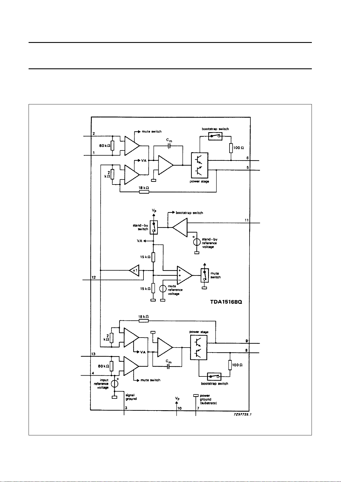
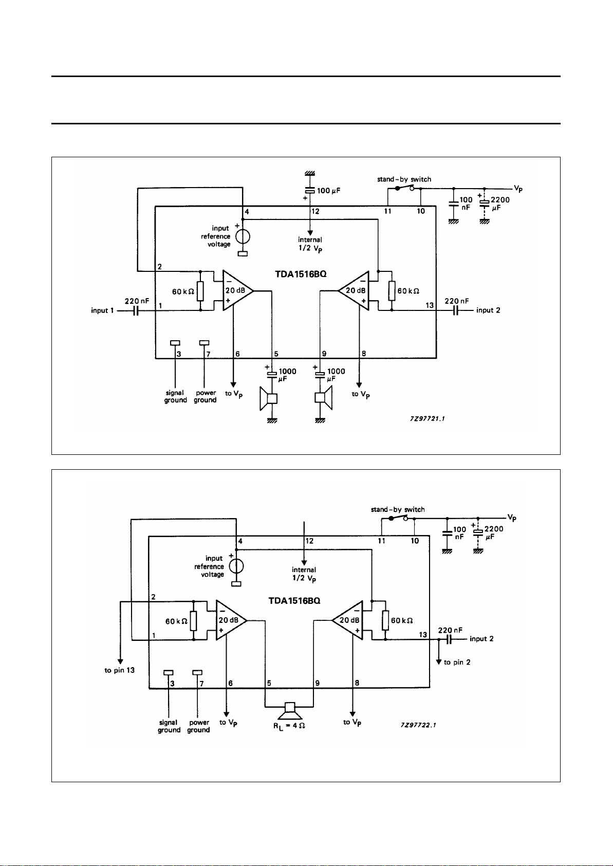
1. All characteristics, for stereo application are measured using the circuit shown in Fig.3.
2. The circuit is d.c. adjusted at VP= 6 V to 18 V and a.c. operating at VP= 8,5 to 18 V.
3. At 18 V < VP< 30 V the d.c. output voltage ≤VP/2.
4. Output power is measured directly at the output pins of the IC.
5. With bootstrap and a 100 kΩresistor from pin 12 to the positive supply voltage (VP), value of bootstrap capacitor is
47 µF.
6. Frequency response externally fixed.
7. Ripple rejection measured at the output with a source impedance of 0 Ω(maximum ripple amplitude of 2 V) and a
frequency between 1 kHz and 10 kHz.
8. Noise voltage measured in a bandwidth of 20 Hz to 20 kHz.
9. Noise output voltage independent of RS(VI= 0 V).
10. All characteristics, for BTL application are measured using the circuit shown in Fig.4.
BTL application note 10
Output power THD = 0,5% Po15,5 17,0 −W
THD = 10% Po20 22 −W
note 5; THD = 10% Po21 24 −W
Output power at VP
= 13,2 V THD = 0,5% Po−13,5 −W
THD = 10% Po−17 −W
note 5; THD = 10% Po−19 −W
Power bandwidth THD = 0,5%
Po= 15 W Bw−20 to −Hz
15 000
Low frequency roll-off note 6;
−3 dB fL−25 −Hz
High frequency roll-off −1 dB fH20 −−kHz
Closed loop voltage gain Gv25 26 27 dB
Supply voltage ripple
rejection: note 7
ON RR 48 −−dB
mute RR 48 −−dB
stand-by RR 80 −−dB
Input impedance |ZI|253038kΩ
Noise output voltage note 8;
ON RS=0ΩVno(rms) −70 −µV
ON RS= 10 kΩVno(rms) −100 200 µV
mute note 9 Vno(rms) −60 −µV
PARAMETER CONDITIONS SYMBOL MIN. TYP. MAX. UNIT

July 1994 9
Philips Semiconductors Product specification
24 W BTL or 2 x 12 watt stereo car radio
power amplifier TDA1516BQ
APPLICATION INFORMATION
Fig.3 Stereo application circuit diagram.
Fig.4 BTL application circuit diagram (without bootstrapping).

July 1994 10
Philips Semiconductors Product specification
24 W BTL or 2 x 12 watt stereo car radio
power amplifier TDA1516BQ
PACKAGE OUTLINE
UNIT A e1
A2bpcD
(1) E(1) Z(1)
deD
hLL
3m
REFERENCES
OUTLINE
VERSION EUROPEAN
PROJECTION ISSUE DATE
IEC JEDEC EIAJ
mm 17.0
15.5 4.6
4.2 0.75
0.60 0.48
0.38 24.0
23.6 20.0
19.6 10 3.4
v
0.8
12.2
11.8 1.7
e2
5.08 2.4
1.6
Eh
62.00
1.45
2.1
1.8
3.4
3.1 4.3
DIMENSIONS (mm are the original dimensions)
Note
1. Plastic or metal protrusions of 0.25 mm maximum per side are not included.
12.4
11.0
SOT141-6
0 5 10 mm
scale
Qj
0.25
w
0.03
x
D
L
E
A
c
A2
m
L3
Q
wM
bp
1
d
D
Ze2
e
e
xh
113
j
E
h
non-concave
view B: mounting base side
92-11-17
95-03-11
DBS13P: plastic DIL-bent-SIL power package; 13 leads (lead length 12 mm) SOT141-6
vM
B

July 1994 11
Philips Semiconductors Product specification
24 W BTL or 2 x 12 watt stereo car radio
power amplifier TDA1516BQ
SOLDERING
Introduction
There is no soldering method that is ideal for all IC
packages. Wave soldering is often preferred when
through-hole and surface mounted components are mixed
on one printed-circuit board. However, wave soldering is
not always suitable for surface mounted ICs, or for
printed-circuits with high population densities. In these
situations reflow soldering is often used.
Thistextgivesavery briefinsightto acomplextechnology.
A more in-depth account of soldering ICs can be found in
our
“IC Package Databook”
(order code 9398 652 90011).
Soldering by dipping or by wave
The maximum permissible temperature of the solder is
260 °C; solder at this temperature must not be in contact
with the joint for more than 5 seconds. The total contact
time of successive solder waves must not exceed
5 seconds.
The device may be mounted up to the seating plane, but
the temperature of the plastic body must not exceed the
specified maximum storage temperature (Tstg max). If the
printed-circuit board has been pre-heated, forced cooling
may be necessary immediately after soldering to keep the
temperature within the permissible limit.
Repairing soldered joints
Apply a low voltage soldering iron (less than 24 V) to the
lead(s) of the package, below the seating plane or not
more than 2 mm above it. If the temperature of the
soldering iron bit is less than 300 °C it may remain in
contact for up to 10 seconds. If the bit temperature is
between 300 and 400 °C, contact may be up to 5 seconds.
DEFINITIONS
LIFE SUPPORT APPLICATIONS
These products are not designed for use in life support appliances, devices, or systems where malfunction of these
products can reasonably be expected to result in personal injury. Philips customers using or selling these products for
use in such applications do so at their own risk and agree to fully indemnify Philips for any damages resulting from such
improper use or sale.
Data sheet status
Objective specification This data sheet contains target or goal specifications for product development.
Preliminary specification This data sheet contains preliminary data; supplementary data may be published later.
Product specification This data sheet contains final product specifications.
Limiting values
Limiting values given are in accordance with the Absolute Maximum Rating System (IEC 134). Stress above one or
more of the limiting values may cause permanent damage to the device. These are stress ratings only and operation
of the device at these or at any other conditions above those given in the Characteristics sections of the specification
is not implied. Exposure to limiting values for extended periods may affect device reliability.
Application information
Where application information is given, it is advisory and does not form part of the specification.
Table of contents
Other Philips Car Amplifier manuals

Philips
Philips CMP200 User manual

Philips
Philips CMQ205 User manual

Philips
Philips TDA1563Q User manual

Philips
Philips TDA1020 User manual

Philips
Philips TDA8567Q User manual

Philips
Philips TDA1561Q User manual

Philips
Philips CID2680 User manual

Philips
Philips TDA8571J User manual

Philips
Philips TDA1552Q User manual

Philips
Philips TDA1519 User manual

Philips
Philips TDA8566 Operational manual

Philips
Philips CMQ205 User manual

Philips
Philips TDA1510AQ User manual

Philips
Philips CMQ405 User manual

Philips
Philips CMP100 User manual

Philips
Philips CMQ205 User manual

Philips
Philips CMQ205 User manual

Philips
Philips CID2680 User manual

Philips
Philips CMP200 User manual