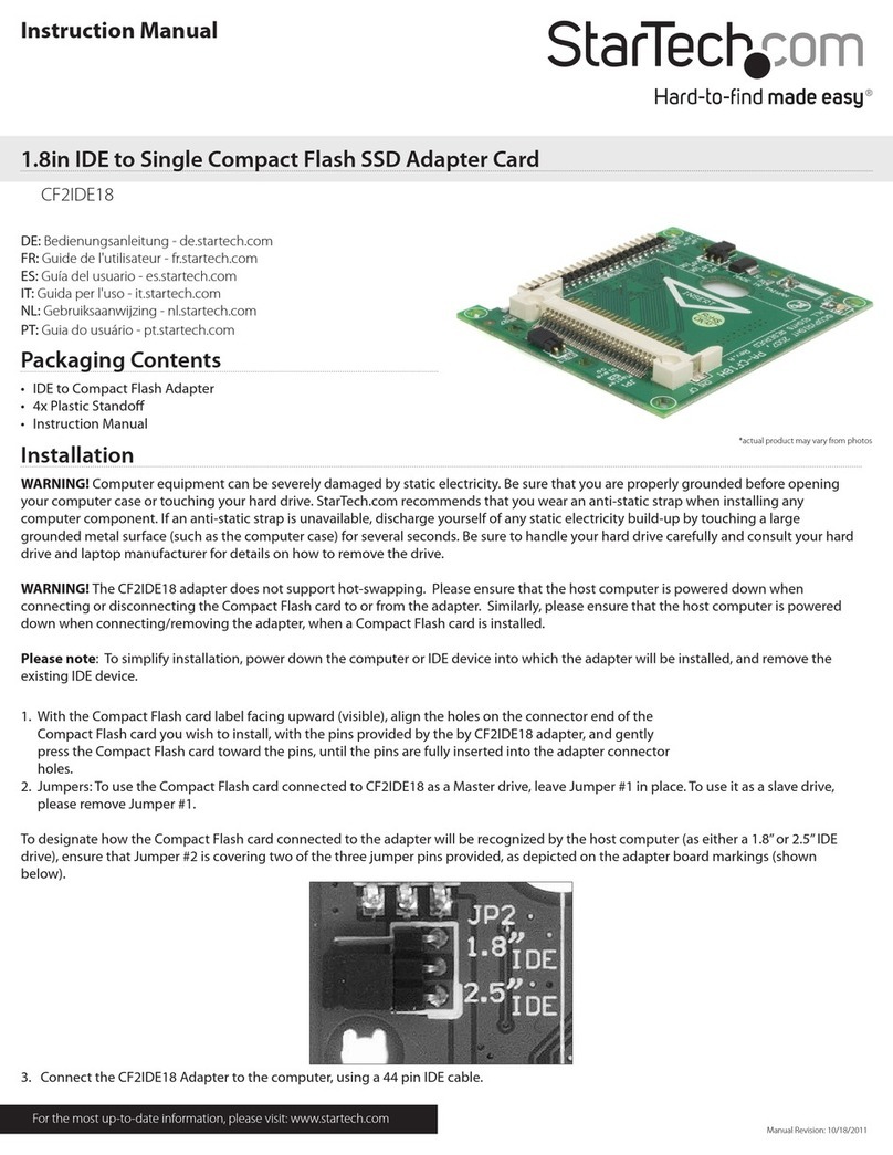
PLX Technology PEX 8618 User manual

PEX 8618
Quick Start Hardware Design Guide
Version 1.2
December 2009
Website: www.plxtech.com
Technical Support: www.plxtech.com/support
Copyright © 2009 by PLX Technology, Inc. All Rights Reserved – Version 1.2
December 18, 2009

PEX 8618 Quick Start Hardware Design Guide – Version 1.2
Copyright © 2009 by PLX Technology, Inc. All rights reserved. ii
© 2009 PLX Technology, Inc. All Rights Reserved.
PLX Technology, Inc. retains the right to make changes to this product at any time, without notice. Products may
have minor variations to this publication, known as errata. PLX assumes no liability whatsoever, including
infringement of any patent or copyright, for sale and use of PLX products.
PLX Technology and the PLX logo are registered trademarks and ExpressLane is a trademark of PLX
Technology, Inc.
Other brands and names are the property of their respective owners.
Document Number: PEX 8618-SIL-DG-1.2
December 18, 2009

PEX 8618 Quick Start Hardware Design Guide – Version 1.2
Copyright © 2009 by PLX Technology, Inc. All rights reserved. iii
Contents
Notice .........................................................................................................................................................v
Revision History..........................................................................................................................................v
1PCI Express Link Interface..................................................................................................................... 1
1.1Transmitter....................................................................................................................................... 2
1.2Receiver........................................................................................................................................... 4
1.3Reference Clock.............................................................................................................................. 4
1.4Spread Spectrum Clocking (SSC)................................................................................................... 6
1.4.1Spread Spectrum Clock Isolation.............................................................................................. 6
1.5Channel ........................................................................................................................................... 7
2PCB Layout and Stackup Considerations.............................................................................................. 8
2.1PEX 8618 BGA Routing Escape and De-Coupling Capacitor Placement....................................... 8
2.2Add-in Board Routing ...................................................................................................................... 9
2.3System Board Routing..................................................................................................................... 9
2.4Midbus Routing.............................................................................................................................. 10
2.5PCB Stackup Considerations........................................................................................................ 10
3Non-Transparent Port Function ........................................................................................................... 11
4Hot-Plug Circuitry................................................................................................................................. 12
5JTAG Interface..................................................................................................................................... 13
6I2C Interface ......................................................................................................................................... 14
7PCI Express Lane Good Indicators...................................................................................................... 14
8Debug Functions.................................................................................................................................. 14
9PEX 8618 Strapping Balls.................................................................................................................... 17
10Power Supplies, Sequencing, and De-Coupling.................................................................................. 18
10.1Power Supplies.............................................................................................................................. 18
10.2Power Sequencing ........................................................................................................................ 18
10.3Board-Level De-Coupling.............................................................................................................. 19
11References........................................................................................................................................... 21

PEX 8618 Quick Start Hardware Design Guide – Version 1.2
Copyright © 2009 by PLX Technology, Inc. All rights reserved. iv
Figures
Figure 1. Sample PCI Express Link Block Diagram..................................................................................1
Figure 2. Single-Ended versus Differential Voltage..................................................................................2
Figure 3. Transport Delay Delta................................................................................................................5
Figure 4. PEX 8618 RefClk Circuit............................................................................................................5
Figure 5. Single Reference Clock Scheme (STRAP_SSC_ISO_ENABLE# pulled high) .........................6
Figure 6. Dual Reference Clock; SSC Crossing Scheme (STRAP_SSC_ISO_ENABLE# pulled low).....7
Figure 7. Add-In Card Routing to PCI Express Gold Fingers ...................................................................9
Figure 8. System Board Routing to PCI Express Slot...............................................................................9
Figure 9. PCI Express Midbus Routing Example....................................................................................10
Figure 10. Enable NT Function with NT Strapping Balls.........................................................................11
Figure 11. Disable NT Function..............................................................................................................11
Figure 12. SHPC Interface to PEX 8618 Block Diagram........................................................................12
Figure 13. JTAG Interface Block Diagram..............................................................................................13
Figure 14. I2C Interface Block Diagram ..................................................................................................14
Figure 15. Power Plane Impedance versus Frequency..........................................................................19
Figure 16. Capacitor Footprint Effects on Series Inductance .................................................................20
Tables
Table 1. Receiver Equalization Settings...................................................................................................4
Table 2. Cross-Reference of Ball Names and Related Debug Signal Names........................................15
Table 3. Strapping Balls..........................................................................................................................17

PEX 8618 Quick Start Hardware Design Guide – Version 1.2
Copyright © 2009 by PLX Technology, Inc. All rights reserved. v
Preface
Notice
This document contains PLX Confidential and Proprietary information. The contents of this document may not be
copied nor duplicated in any form, in whole or in part, without prior written consent from PLX Technology, Inc.
PLX provides the information and data included in this document for your benefit, but it is not possible to entirely
verify and test all the information, in all circumstances, particularly information relating to non-PLX manufactured
products. PLX makes neither warranty nor representation relating to the quality, content, or adequacy of this
information. The information in this document is subject to change without notice. Although every effort has been
made to ensure the accuracy of this manual, PLX shall not be liable for any errors, incidental or consequential
damages in connection with the furnishing, performance, or use of this manual or examples herein. PLX assumes
no responsibility for damage or loss resulting from the use of this manual, for loss or claims by third parties, which
may arise through the use of the PEX 8618, or for any damage or loss caused by deletion of data as a result of
malfunction or repair.
Revision History
Date Version Comments
July 2008 0.1 Preliminary Release
October 2008 1.0 Initial Release
November 2008 1.1 Updated Table2
Updated Table 3
Other Text Edits
December 2009 1.2 Made corrections to section 1.4.1

Introduction
This quick start hardware design guide is an overview of PLX Technology’s ExpressLane™ PEX 8618 PCI
Express Switches and provides examples of how to connect to the various switch interfaces.
1 PCI Express Link Interface
PLX’s PEX 8618 is a 16-Lane, 16-Port PCI Express 2.0 (Gen 2) compliant switch. PCI Express 2.0 supports
transfer rates of 2.5 GT/s and 5.0 GT/s per Lane. The PEX 8618 supports the required 2.5 GT/s as well as the
optional 5.0 GT/s on its physical interface. The Physical Media Attachment (PMA) Layer for each Lane is
implemented as a SerDes transceiver, which is composed of a transmit path and receive path. The transmit path
typically contains a serializer, Phase Lock Loop (PLL), and Current Mode Logic (CML) driver. The receive path
consists of a CML Receiver buffer, Clock and Data Recovery circuit (CDR), and a de-serializer.
As the PCI Express Base Specification, Revision 2.0, continues to mature, so does its description of the Physical
Layer Electrical sub-block. A PCI Express serial Link is described in terms of four components – Transmitter,
Receiver, Channel, and Reference Clock. The Transmitter and Receiver elements are typically integrated into PCI
Express silicon. The channel and Reference Clock are implemented at the system level. The PCI Express
interoperability matrix implies that all four elements must support 5.0 GT/s for the Link to successfully run at
5.0 GT/s. If any one element is not 5.0 GT/s-compliant, the Link will not be able to operate beyond 2.5 GT/s.
Another important concept is that 2.5 GT/s is not a subset of 5.0 GT/s. This implies that a design targeted to meet
5.0 GT/s might not successfully run in a 2.5 GT/s environment, if those design criteria are not met, as well.
Figure 1 illustrates a block diagram of a sample PCI Express Link.
PLL1
CDR1 PLL2
CDR2
RefClk
Rx1
Rx2Tx1
Tx2
Channel
Channel
Device 1 Device 2
Figure 1. Sample PCI Express Link Block Diagram
PEX 8618 Quick Start Hardware Design Guide – Version 1.2
Copyright © 2009 by PLX Technology, Inc. All rights reserved. 1

1.1 Transmitter
A PCI Express Transmitter is typically a differential CML driver that transmits an 8b/10b encoded bit-stream
across the channel to the Receiver. The minimum differential voltage swing (VTX-DIFF-PP) of the Transmitter is
800 mV at both 2.5 GT/s and 5.0 GT/s. The DC common mode voltage can be anywhere between 0 and 3.6V;
hence, AC-coupling capacitors are required to isolate the Transmitter’s DC component from the Receiver’s fixed
0V DC common mode voltage. The AC-coupling capacitor values must range between 75 nF and 200 nF, to
ensure that the lower frequency components of the 8b/10b encoded data are not affected. Figure 2 illustrates
what a generic PCI Express differential signal looks like, as compared to a single-ended signal.
Note: The swing values listed in Figure 2 (400 mV and 800 mV) do not reflect default PLX register values.
PCI Express Transmitters are required to support de-emphasis. The role of de-emphasis is to reduce the amount
of energy used to transmit multiple successive bits of the same polarity (that is, non-transition bits), compared to
the amount of energy used to transmit a set of transition bits (0 -> 1 or 1 -> 0). Transition bits have higher
frequency components than non-transition bits and are, therefore, more distorted by the low-pass channel. This
effect is also known as Inter-Symbol Interference (ISI), which is a source of deterministic jitter in the system.
The PCI Express Base Specification, Revision 2.0 defines two de-emphasis levels for devices running at
5.0 GT/s, 3.0 to 4.0 dB and 5.5 to 6.5 dB. The desired de-emphasis level for a given Link is advertised by the
downstream Ports of a switch during Link recovery. Endpoints and switch upstream capture this value and Set
their de-emphasis level, accordingly. Longer Links should use 6.0 dB, whereas shorter Links can use the 3.5 dB
level.
The standard de-emphasis level is selectable by way of the PEX 8618 Link Control 2 register Selectable De-
Emphasis bit (Configuration register, offset 98h[bit 6]).
TXp
PEX 8618 Quick Start Hardware Design Guide – Version 1.2
Copyright © 2009 by PLX Technology, Inc. All rights reserved. 2
Figure 2. Single-Ended versus Differential Voltage
In addition to supporting the standard de-emphasis levels, the PEX 8618 has a number of programmable
registers to control the Transmitter’s characteristics, such as drive level and de-emphasis. Registers at offsets
B98h to BA4h are the SerDes Drive Level registers. Registers at offsets BA8h to BB4h are the Post-Cursor
Emphasis Level registers. The SerDes Drive Level and Post-Cursor Emphasis Level registers work in
conjunction, to determine the transition and non-transition bits driver swing and de-emphasis ratio. The PLX driver
is implemented as a two-tap driver. When transition bits are transmitted, the SerDes Drive Level and Post-
Cursor Emphasis Level register levels are added together; for non-transition bits, the two values are subtracted.
Using Equation 1, Example 1 presents a calculation of what the drive level and de-emphasis level would be for a
given set of register values.
TXn
VTX-DC-CM
TXp - TXn
400mV
800mV
0V

PEX 8618 Quick Start Hardware Design Guide – Version 1.2
Copyright © 2009 by PLX Technology, Inc. All rights reserved. 3
Systems with short Links and/or power-sensitive applications (such as mobile platforms) can optionally decide to
use low-swing output drive levels (400 mVP-P). In the PEX 8618, this can be accomplished by setting the SerDes
Drive Level register for a specific Lane to 01000b (400 mVP-P), and the Post-Cursor Emphasis Level register to
00000b (no de-emphasis).
Equation 1. PEX 8618 Transmitter Drive Level
(a) VTRANS = VDRV_LVL + VPOST_EMP
(b) VNON-TRANS = VDRV_LVL - VPOST_EMP
(c) VTX-DE-RATIO-3.5DB = 20 log (VNON-TRANS/ VTRANS)
Example 1. Setting for Lane 0 Transmitter to 3.5 dB
Port 0 SerDes Drive Level register, offset B98h[4:0] = 01111b (750 mVpp)
Port 0 Post-Cursor Emphasis Level register, offset BA8h[4:0] = 01101b (162.5 mVpp)
VTRANS = 750 mV + 162.5 mV = 912.5 mVpp
VNON-TRANS = 750 mV - 162.5 mV = 587.5 mVpp
VTX-DE-RATIO-3.5 DB = 20 log (587.5/912.5) = -3.82 dB

PEX 8618 Quick Start Hardware Design Guide – Version 1.2
Copyright © 2009 by PLX Technology, Inc. All rights reserved. 4
1.2 Receiver
The Receiver’s role is to recover the differential bit-stream coming across the channel from the Transmitter, and
latch it so it can be de-serialized and forwarded to the logical sub-block. The main components of a Receiver are
the receive buffer and the CDR circuit.
The PCI Express receive buffer input threshold is 175 mV for 2.5 GT/s data rate and 120 mV for a 5.0 GT/s data
rate. PCI Express Receivers are required to have a DC common mode voltage of 0V.
The receive buffer will provide bits to the CDR circuit, which samples each bit and forwards to the de-serializer.
Digital-based CDRs must track the edges of the incoming bits and determine the best time to sample each bit,
which is typically the center of eye (0.5 UI). The CDRs base Reference Clock(s) is provided by the PLL. A CDR
must be able to track either a fixed phase offset (common clock system) or small continuous phase offset (non-
common clock system) between the incoming data/clock and the CDRs base clock. Jitter on the base CDR clock
and/or the incoming data stream can cause bit sampling errors to occur.
Although not explicitly mentioned in the PCI Express specification, Receivers may implement some form of
Receiver equalization to help compensate for the low-pass characteristics of the channel. In general, Receiver
equalization only needs to be used on longer channels.
The PEX 8618 provides a programmable receive equalization function. Each port has a set of Receiver
Equalizer registers, located at offsets BB8h and BBCh, to control a group of 16 SerDes. Each individual SerDes
has a 4-bit control word. Table 1 describes the Receiver equalization effects.
Table 1. Receiver Equalization Settings
SerDes NReceiver Equalizer[3:0] Equalization
0000b Off
0010b Low
0110b Medium
1110b High
1.3 Reference Clock
The Reference Clock is a key component to a Link that was often overlooked by system designers in first
generation PCI Express systems. The Reference Clock provides a 100 MHz base frequency for the PLL. The PLL
provides a frequency synthesis function, generating the higher speed clocks required to transmit data at a rate of
either 2.5 GT/s or 5.0 GT/s. In designs that implement digital CDRs, the PLL output also provides the Reference
Clocks to the CDR circuit; hence, jitter on the Reference Clock can affect both the Transmitter and Receiver
components.
The PLL has a low-pass, jitter-filter transfer function from its reference input to the high speed output clocks;
therefore, it is important to minimize the low-frequency jitter in the pass band of the PLL. Low-frequency jitter
below the PLL loop bandwidth passes directly to output clocks, which, in turn, drives the Transmitter and CDR
circuits. Jitter at the loop bandwidth is especially critical, given most PLLs have some amount of gain at the cut-off
frequency. High-frequency jitter on the Reference Clock input above the loop bandwidth is typically attenuated,
and is therefore of less concern.
The jitter transfer function of a CDR circuit is modeled as a high-pass filter. Low-frequency jitter, including Spread-
Spectrum Clock (SSC) modulation, is tracked by the CDR circuit, whereas higher-frequency jitter content causes
eye closure at the Receiver. The cut-off frequency of the CDR high-pass function is usually less than the cut-off
frequency of the Transmitter PLL low-pass function. The pass band between these cut-off frequencies is where
Reference Clock jitter causes the most problems.
In PCI Express, the cut-off frequency of the PLL is specified to be between 1.5 to 22 MHz for 2.5 GT/s and 8 to
16 MHz for 5.0 GT/s data rates. The purpose of these bandwidth ranges is to limit the difference in PLL bandwidth
on the two sides of a Link. This is especially important for common clock systems, where the amount of jitter
appearing at the CDR is defined by the difference function between the Tx and Rx PLLs.
Another mechanism that can increase jitter seen by a Receiver in common clocked systems is the fixed phase
difference (transport delay delta) between Transmitter data at the CDR input and a Receiver’s recovered clock,
relative to the 100 MHz Reference Clock source. This delay should not exceed 12ns per PCI Express
specification. The delay budget includes on-chip and off-chip delays. In general terms, all Reference Clock nets in
a system should be matched within 38.1 cm (15 in.). Figure 3 illustrates Reference Clock transport delay delta.
The PEX 8618 PEX_REFCLKn/p signal is the Reference Clock Input buffer. It has an internal DC-biasing circuit,
and hence, should be AC-coupled from the RefClk source driver. Use 0.01 to 0.1 µF capacitors (0603 or 0402-
size) to AC-couple the Reference Clock input, as illustrated in Figure 4.
PLL1
CDR1 PLL2
CDR2
RefClk
Rx1
Rx2Tx1
Tx2
Channel
Channel
Device 1 Device 2
T1
T2
T3
T4
T5
Transport Delay Delta = (T1+T2+T3) – (T4+T5) < 12 ns
Figure 3. Transport Delay Delta
Figure 4. PEX 8618 RefClk Circuit
PEX 8618 Quick Start Hardware Design Guide – Version 1.2
Copyright © 2009 by PLX Technology, Inc. All rights reserved. 5

1.4 Spread Spectrum Clocking (SSC)
Many PCI Express systems implement spread spectrum clocking in order to minimize EMI by spreading the
spectral energy of the clock signal over a wide frequency band. In SSC systems, PCI Express components
generally need to use a reference clock provided by the same source. This allows a transmitter PLL and receiver
clock recovery function (CDR) to track the modulation frequency and stay in sync with each other. If only one side
of the link uses a SSC reference clock and the other side does not, the transmitter and receiver circuits will not be
able to properly track one another. For example, if a system designer implements a PCI Express add-in card that
interfaces to an SSC system and also has a cable connection to a downstream card that is utilizing a constant
frequency clock source (CFC), the downstream interface will not link-up. To solve this problem, a system designer
using the PEX 8618 can either use the SSC isolation feature (explained in section 1.4.1) or provide a means to
pass the SSC clock to the downstream component.
1.4.1 Spread Spectrum Clock Isolation
The PEX 8618 provides a new feature that helps eliminate the issues that exist when trying to communicate
between two different systems, where one or both of those systems use SSC clocking.
The PEX 8618 has the necessary buffering and logic required to allow the upstream port to operate using both an
SSC clock and a constant frequency clock (CFC) source. This feature is enabled when the signal
STRAP_SSC_ISO_ENABLE# is pulled down to VSS. In order to use the SSC isolation feature, the upstream port
must be port 0, and its programmed port width must be x4 or x8.
Enabling this feature provides the benefit of allowing downstream components to operate using an independent
CFC clock source. If a PEX 8618 is placed into a system that uses spread spectrum clocking, and the SSC
isolation feature is enabled, the downstream ports of the PEX 8618 will be clocked by a CFC clock source.
System designers can then connect to a remote system without the requirements of sharing a reference clock
source. The remote system must utilize a CFC clock source that meets the PCI Express +/-300ppm requirements.
Figure 5 depicts running the PEX 8618 using the standard distributed clocking scheme for PCI Express. If SSC
isolation is not used, the PEX_REFCLK_CFCp/n inputs can be left unconnected.
PEX 8618
Port 0
Port 1 . . . Port N
VDD25
PEX
_
REFCLKp/n
Upstream
STRAP_SSC_ISO_ENABLE#
Downstream
Device
RefClk
Generator
(If SSC then required
to be from same
source)
Downstream
Device
Device
Figure 5. Single Reference Clock Scheme (STRAP_SSC_ISO_ENABLE# pulled high)
PEX 8618 Quick Start Hardware Design Guide – Version 1.2
Copyright © 2009 by PLX Technology, Inc. All rights reserved. 6

Figure 6 demonstrates a mixed SSC and CFC system that might exist when utilizing PEX 8618’s SSC isolation
feature. NOTE: When SSC isolation is used, the SSC clock must be connected to PEX_REFCLKp/n.
PEX 8618
Port0
Port 1 . . . Port N
VSS
PEX
_
REFCL
K
_
CFCp/n
PEX
_
REFCLKp /n
Spread Spectrum Clock
(SSC)
Constant Frequency Clock
(CFC) environment
Upstream
Downstream
Device
Downstream
Device
1
RefClk
Generato
r
REFCLKp /n
REFCLKp /n
(Not required to be romf
same source )
2
RefClk
STRAP_SSC_ISO_ENABLE#
Generato
r
Device
Figure 6. Dual Reference Clock; SSC Crossing Scheme (STRAP_SSC_ISO_ENABLE# pulled low)
1.5 Channel
In PCI Express, the channel refers to the board level copper interconnects (including connectors) that lie between
the Transmitter and Receiver balls. The channel is represented as a transmission line, which can be modeled by
a distributed series of Resistance Inductance Conductance Capacitance (RLGC) circuits. A transmission line
behaves like a low-pass filter due to frequency-dependent dielectric and conductor losses.
In PCI Express, the channel contributes to amplitude loss and deterministic jitter. It is important to minimize
discontinuities, such as vias and stubs, to minimize channel effects.
A common issue that presents itself to PCI Express system designers is determining allowable channel length.
This is a question that does not have a simple answer. The best way to determine if a particular channel length is
allowable is to simulate the channel using PLX provided HSPICE models. The PCI Express Base Specification,
Revision 2.0 provides additional details for simulating a channel.
PEX 8618 Quick Start Hardware Design Guide – Version 1.2
Copyright © 2009 by PLX Technology, Inc. All rights reserved. 7

PEX 8618 Quick Start Hardware Design Guide – Version 1.2
Copyright © 2009 by PLX Technology, Inc. All rights reserved. 8
2 PCB Layout and Stackup Considerations
PCB layout is of critical importance for PCI Express systems. Numerous form factor specifications (PCI Express
Base Specification, Revision 2.0 and PCI Express Card Electromechanical (CEM) Specification, Revisions 1.0a
and 1.1) exist for providing important implementation guidelines for a given form factor. It is important to
understand the type of system being designed before starting layout. For example, the PCI Express Card
Electromechanical (CEM) Specification defines two platforms, referred to as system boards and add-in cards
(boards). Each platform has its own criteria, in terms of jitter and loss budget, trace lengths and length matching,
and so forth.
2.1 PEX 8618 BGA Routing Escape and De-Coupling Capacitor Placement
One millimeter pitch BGA package routing can typically escape two rows of balls per signal layer. Power and
ground pads typically have small “dog-bone” nets from the pad to a via which will connect it with an internal power
or ground plane. The PEX 8618 places all Transmitter differential pairs on the outer two rows of balls and
Receiver differential pairs on rows three and four. This means it should take two signal layers in a PCB stackup to
escape the differential pairs from the BGA. All Transmitters can escape on the top layer of a PCB, whereas the
Receiver pairs can escape on either the bottom layer or some other internal signal layer.
Each pair is split between two rows on the package; hence, the pairs start off with a 1-mm (39.4-mil) offset. Small
serpentines may be necessary to match the lengths within the pair. If the differential pairs are tightly coupled,
make the serpentines as close to the launching end of the channel as possible, to allow the differential signal to
be tightly coupled as it travels down the channel. If uncoupled differential pairs are used, only the total
propagation delay of each half of the pair needs to be matched. This makes using uncoupled differential pairs
simpler to route. There are two disadvantages to using uncoupled differential pairs; they take more board real
estate to route, and they are not as immune to common mode noise.
The PEX 8618 is a full matrix, 1-mm pitch BGA. Hence, placing de-coupling capacitors underneath the BGA can
be tricky. It is best to use 0201-sized ceramic capacitors under the BGA matrix (bottom layer), so that the
capacitors can be placed as close to the power balls as possible. Refer to section 10.3 for more details.

2.2 Add-in Board Routing
The PEX 8618 Transmitter pairs escape on the top layer, but at some point must route to the bottom layer, to
connect to the gold fingers. If a logic analyzer midbus footprint is placed in the routing path, the layer transition
can occur at that point. This works out well, because the midbus footprint will have a significant number of ground
vias, which provide effective ground plane stitching for the differential signal’s return path. If a midbus footprint is
not used, layer changing can occur at the AC-coupling capacitors. Dedicated ground vias can be placed near the
capacitors, close to the signal vias, to provide a return path. One ground via per pair is ideal; however, one via per
every two pair is acceptable.
Receiver differential pairs must also transition signal layers, at least one time. Receiver pairs start off at the top
layer, from the gold fingers, and into the inner rows of the BGA. To avoid routing congestion, it is ideal to have the
receiver and transmission pairs transition layers at roughly the same point. In any situation, the transition
locations should have plenty of stitching ground vias.
PCI Express add-in boards must be length-matched within 5-mil. Differential pairs for PCI Express Gen 2 add-in
boards should have a differential impedance of between 68 to 105 ohms (85 ohms, nominal).
Figure 7. Add-In Card Routing to PCI Express Gold Fingers
2.3 System Board Routing
System board routing is simplified slightly. Transmitter pairs can escape on the top layer from the BGA and route
to AC-coupling capacitors. Similarly, Receiver pairs can escape on the bottom layer and directly route to the slot.
Transmitter pairs can also transition to the bottom layer after the AC-coupling capacitors, to minimize the stub
effects of a through-hole PCI Express slot.
PCI Express system boards must be length-matched within 10-mil. Differential pairs for PCI Express Gen 2
system boards should have differential impedance between 68 to 105 ohms (85 ohms, nominal).
Figure 8. System Board Routing to PCI Express Slot
PEX 8618 Quick Start Hardware Design Guide – Version 1.2
Copyright © 2009 by PLX Technology, Inc. All rights reserved. 9

2.4 Midbus Routing
Midbus footprints can be placed into the routing path, to provide an interface to various protocol analyzers, as well
as provide a location to probe a signal using oscilloscopes. Transmitter pairs route on one side of the footprint,
while Receiver signals route through the other side.
Figure 9. PCI Express Midbus Routing Example
2.5 PCB Stackup Considerations
Determining the PCB stackup is one of the most important steps in designing and implementing a system. The
PCB stackup should be determined prior to board routing, because it will determine the trace width and spacing
requirements necessary to achieve a particular characteristic impedance and differential impedance. After the
stackup is known, the trace width can be selected. For a single-ended signal, this is enough to determine the
characteristic impedance of that trace. For differential signals, the last step is to determine the separation
between the positive and negative conductors, to achieve the needed differential impedance.
Additionally, a PCB stackup can determine the power supply de-coupling scheme for a device. Parallel plane
capacitance exists between a PCB’s DC power and ground planes. PCB reference planes have an insignificant
amount of series inductance; therefore, their effective frequency range is much higher than that of
discrete capacitors.
PCB traces can be implemented as one of two types of transmission lines – microstrip and stripline. Microstrip
traces have only one reference plane, and therefore, represent traces on the outer layers (top and bottom layer)
of a PCB. Stripline traces have two reference planes and are implemented using inner routing layers. Typically,
stripline traces are only available for PCBs with six or more layers. Microstrip and stripline traces each have their
own properties, which must be weighed when determining which type of trace to use.
PEX 8618 Quick Start Hardware Design Guide – Version 1.2
Copyright © 2009 by PLX Technology, Inc. All rights reserved. 10

3 Non-Transparent Port Function
The PEX 8618 supports Non-Transparent mode (NT mode) function. Any of the possible 16 Ports can be
configured as the NT Port.
There are three ways to enable the NT function and configure the NT Port for the PEX 8618.
Method 1. Use of the five Strapping balls:
STRAP_NT_ENABLE#
STRAP_NT_UPSTREAM_PORTSEL[3:0]
Pull down the STRAP_NT_ENABLE# to logic zero (0) to enable the NT function. Pull up or down the
STRAP_NT_UPSTREAM_PORTSEL[3:0] to select the NT Port. Make sure the NT port selected is NOT the same
as the upstream port.
Method 2. Enable the NT function and configure the NT Port through the serial EEPROM, when the PEX 8618
switch is powering up.
Method 3. Use the PEX 8618 I2C Port 0 to enable the NT function and configure the NT Port. Figure 10
illustrates how to implement the NT functions through the Strapping balls. Figure 11 illustrates how to disable the
NT functions, through the PEX 8618’s NT Strapping balls.
Figure 10. Enable NT Function with NT Strapping Balls
Figure 11. Disable NT Function
PEX 8618 Quick Start Hardware Design Guide – Version 1.2
Copyright © 2009 by PLX Technology, Inc. All rights reserved. 11

4 Hot-Plug Circuitry
The PEX8618 device supports Hot-Plug through a serial Hot-Plug interface brought out through I2C port 1. By
connecting I2C to multiple I/O expander ICs, the PEX 8618 has the option of having Hot-Plug capability on all
fifteen of its downstream Ports. The PEX 8618’s I2C Port 1 is the I2C Master, which is designed to interface to I/O
expander ICs, to build SHPCs. One 16-I/O expander connects to I2C Port 1 for a single SHPC, and one 40 I/O
expander connects to the I2C Port 1 for two SHPCs. 16-I/O expander(s) and 40-I/O expander(s) cannot
concurrently connect to the I2C Bus. To use 40-I/O expander(s), a register bit within the PEX 8618 must be Set,
and boot with serial EEPROM is essential. After the PEX 8618 is powered up, the state machine inside the PEX
8618 scans the number of I/O expander ICs connecting to the I2C Bus, starting from Address 000h, in ascending
order. If it cannot locate the device with Address 000h, it stops the scan process. After it locates the I/O expander
IC, it automatically assigns a valid Port Number for this SHPC. Figure 12 illustrates a block diagram of the SHPC
interface to the PEX 8618. Besides the 10 standard Hot-Plug signals, INTERLOCK, SLOTID[3:0], and one GPIO
are added to the SHPC. Also, the interrupt signal output, INT#, from the I/O expander, should be connected to the
PEX 8618’s Interrupt Input ball, SHPC_INT#, for the PEX 8618 to service input events at the SHPC.
Figure 12. SHPC Interface to PEX 8618 Block Diagram
PEX 8618 Quick Start Hardware Design Guide – Version 1.2
Copyright © 2009 by PLX Technology, Inc. All rights reserved. 12

5 JTAG Interface
The PEX 8618 supports a five-ball JTAG Boundary Scan interface. The JTAG interface consists of the following
signals:
JTAG_TCK
JTAG_TMS
JTAG_TDI
JTAG_TDO
JTAG_TRST#
At the board level, pull JTAG_TDI, JTAG_TMS, and JTAG_TCK up to 2.5V with 1-kohm to 5-kohm resistors. Pull
JTAG_TRST# down to VSS with a 1-kohm to 5-kohm resistor. Because the PEX 8618 JTAG clock frequency can
be as high as 25 MHz, a 15-ohm series terminator can be added to TCK, TDI, and TDO, to improve signal quality.
Figure 13 illustrates a generic JTAG interconnection.
Figure 13. JTAG Interface Block Diagram
PEX 8618 Quick Start Hardware Design Guide – Version 1.2
Copyright © 2009 by PLX Technology, Inc. All rights reserved. 13

6 I2C Interface
The PEX 8618 also implements a two-wire I2C Slave interface (I2C Port 0). Through its I2C_SCL0 and I2C_SDA0
balls, the PEX 8618 allows an external I2C Master to read and write device registers through an out-of-band
mechanism. The I2C slave address is 0111xxx, with the lower 3 bits being determined by the values on Strapping
balls I2C_ADDR[2:0]. The simplest way to implement an I2C interface to the PEX 8618 is illustrated in Figure 14 .
Figure 14. I2C Interface Block Diagram
7 PCI Express Lane Good Indicators
The PEX 8618 provides 16 Active-Low “Lane Good” Output balls for each PCI Express Lane on the device.
These Output balls can be used to indicate the status of each PEX 8618 Lane. If a given Lane Good indicator is
continually asserted, that lane is up and operating at 5 GT/s. If a given Lane Good indicator is blinking, that lane is
up and operating at 2.5 GT/s.
8 Debug Functions
(The optional Debug function is primarily intended for prototyping activities. Its use requires assistance from PLX
Technical Support.)
Two major debug functions of the PEX 8618 are External Probe mode (EPM) and SerDes Debug mode (SDM).
The EPM function is for viewing the internal state machines and control signals of the station-based modules and
the core-based module. The SDM function is for viewing the 20-bit Receive Bus (elastic buffer exit) and 20-bit
Transmit Bus of each Lane of the SerDes, in the PEX 8618. Two Strapping balls are used to enable either Debug
mode function. Pulling down the STRAP_PROBE_MODE# ball enables the EPM function. Pulling down the
STRAP_SERDES_MODE_EN# ball enables the SDM function. The EPM contains 18 inputs and 38 outputs. The
SDM contains 7 inputs and 45 outputs. When either Debug mode is enabled, the EPM and SDM inputs and
outputs are serviced by most of the General-Purpose I/O balls, the Spare balls, as well as other control and status
balls such as PEX_LANE_GOOD and STRAPPING balls. Table 2 cross-references the ball names and their
related Debug signal names.
Notes: Inputs are marked in blue, outputs are marked in red.
The maximum frequency of Debug mode Output signals, such as PROCMON (N/C, at location T6), is 125 MHz,
with fast rise and fall time. When routing these traces to the mictor connector for scope probing, 50-ohm, single-
ended controlled-impedance traces are recommended. To service normal operation and debug functions, low-
capacitive load bus switches can be used to prevent the reflections. For example, a bus switch can be used to
separate the LED circuit from the PEX_PORT_GOODx# signals, when they are used as outputs of Debug mode
signals.
PEX 8618 Quick Start Hardware Design Guide – Version 1.2
Copyright © 2009 by PLX Technology, Inc. All rights reserved. 14

PEX 8618 Quick Start Hardware Design Guide – Version 1.2
Copyright © 2009 by PLX Technology, Inc. All rights reserved. 15
Table 2. Cross-Reference of Ball Names and Related Debug Signal Names
Ball Name Probe Mode SerDes Debug Mode
STRAP_NT_UPSTRM_PORTSEL2 stn_sel
STRAP_DEBUG_SEL0 mod_sel3 In_sel3
STRAP_UPCFG_TIMER_EN# mod_sel2 rcvr_dat18
STRAP_SMBUS_EN# mod_sel1 In2_add1
STRAP_SPARE0# mod_sel0 In2_add0
I2C_ADDR2 port_sel3 In_sel0
GPIO30 port_sel2 In_sel2
GPIO29 port_sel1 In_sel1
STRAP_NT_UPSTRM_PORTSEL3 port_sel0
GPIO3 outA_sel3 rx_status0
GPIO2 outA_sel2
GPIO1 outA_sel1
GPIO0 outA_sel0
I2C_ADDR1 outB_sel3
I2C_ADDR0 outB_sel2
GPIO5 outB_sel1 rx_status2
GPIO4 outB_sel0 rx_status1
STRAP_SPARE1# ext_trig_in rcvr_polarity
PEX_LANE_GOOD15# prb_outA17 rcvr_dat17
PEX_LANE_GOOD14# prb_outA16 rcvr_dat16
PEX_LANE_GOOD13# prb_outA15 rcvr_dat15
PEX_LANE_GOOD12# prb_outA14 rcvr_dat14
PEX_LANE_GOOD7# prb_outA13 rcvr_dat13
PEX_LANE_GOOD6# prb_outA12 rcvr_dat12
PEX_LANE_GOOD5# prb_outA11 rcvr_dat11
PEX_LANE_GOOD4# prb_outA10 rcvr_dat10
GPIO15 prb_outA9 rcvr_dat9
GPIO14 prb_outA8 rcvr_dat8
GPIO13 prb_outA7 rcvr_dat7
GPIO12 prb_outA6 rcvr_dat6
GPIO11 prb_outA5 rcvr_dat5
GPIO10 prb_outA4 rcvr_dat4
GPIO9 prb_outA3 rcvr_dat3
GPIO8 prb_outA2 rcvr_dat2
GPIO7 prb_outA1 rcvr_dat1
GPIO6 prb_outA0 rcvr_dat0
GPIO25 prb_outB17 xmit_dat17
GPIO24 prb_outB16 xmit_dat16
GPIO23 prb_outB15 xmit_dat15
GPIO22 prb_outB14 xmit_dat14
GPIO21 prb_outB13 xmit_dat13
GPIO20 prb_outB12 xmit_dat12
GPIO19 prb_outB11 xmit_dat11
GPIO18 prb_outB10 xmit_dat10
GPIO17 prb_outB9 xmit_dat9
GPIO16 prb_outB8 xmit_dat8
PEX_LANE_GOOD11# prb_outB7 xmit_dat7
PEX_LANE_GOOD10# prb_outB6 xmit_dat6
PEX_LANE_GOOD9# prb_outB5 xmit_dat5
Table of contents
Other PLX Technology Computer Hardware manuals

PLX Technology
PLX Technology PEX 8615 User manual

PLX Technology
PLX Technology PEX 8114RDK-R Quick user guide

PLX Technology
PLX Technology CompactPCI 9030RDK-LITE Quick user guide

PLX Technology
PLX Technology PEX 8606 User manual

PLX Technology
PLX Technology PEX 8604 User manual

PLX Technology
PLX Technology PEX 8548-AA RDK Quick user guide
Popular Computer Hardware manuals by other brands

Acrosser Technology
Acrosser Technology AR-B2001 manual

National Instruments
National Instruments PXI/CompactPCI Embedded Computer NI PXI-8108 user manual

Cypress
Cypress CY8CKIT-029 PSoC quick start guide

Exsys
Exsys EX-6069-2 manual

GE
GE Profibus - DP Bus instructions

Kodak
Kodak X-Omat 270 RA PROCESSOR installation instructions