RL78/G10 ターゲット・ボード
RTE510Y470TGB00000R ユーザーズ・マニュアル
ユーザーズ・マニュアル
R20UT2894XJ0100
Rev 1.00 2014.2.28
本製品は、ルネサス エレクトロニクス製のプログラミング機能付きオンチップ・デバッグ・エミュレータ E1 を使用して、マイコンの動作を試
すためのターゲット・ボードです。
①RL78/G10 ターゲット・ボード(RTE510Y470TGB00000R)の特徴
●RL78/G10(R5F10Y47)搭載
●20MHz の発振子を搭載
●ユニバーサル・エリア(2.54mm ピッチ)を搭載
●フラッシュ・メモリ・プログラミング, オンチップ・デバッグの両方に対応(TOOL0 端子使用)
●マイコンの端子を周辺ボード・コネクタに配置した高拡張性
●基板を切り離すことで, 2.54 ㎜DIP ピッチに変換した基板として使用可能
CPU R5F10Y47 メイン・クロック動作周波数 20MHz
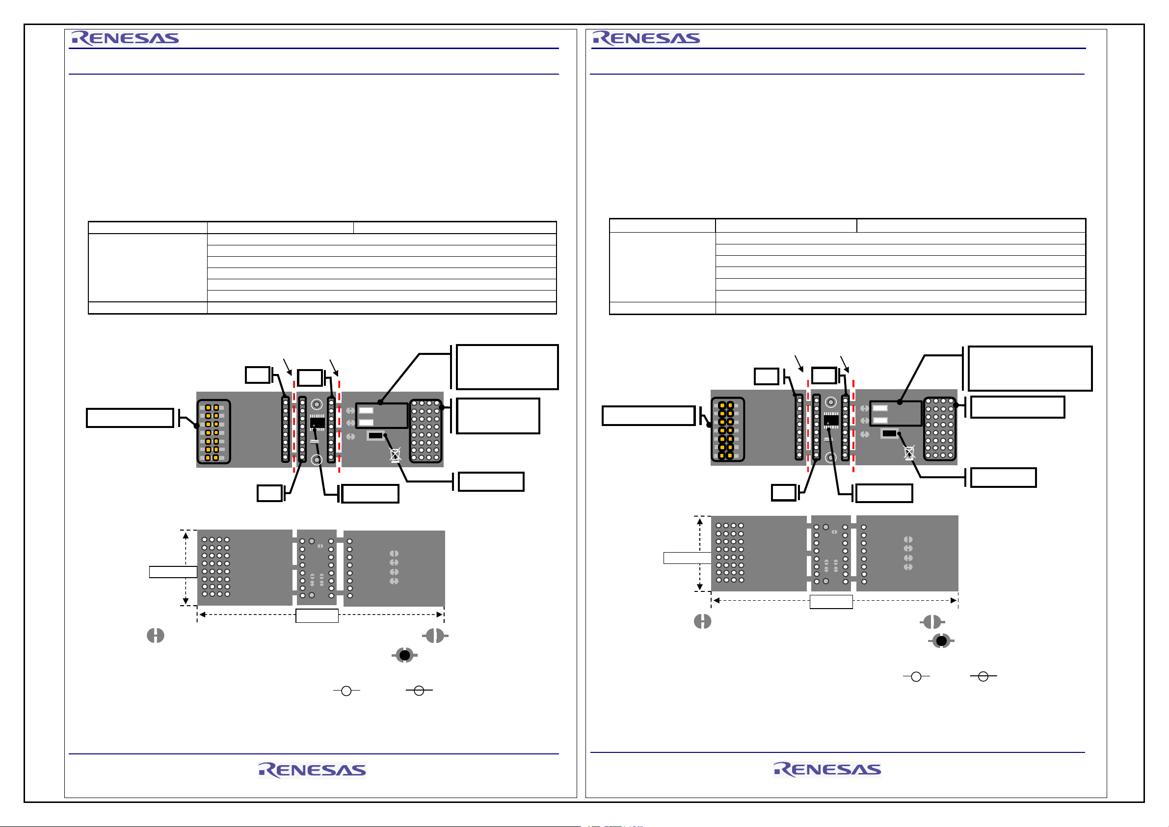
搭載部品
CN1,CN2,CN4: 周辺ボードコネクタ(2.54mm ピッチ) 8pin ソケット x3(パッドのみ)
CN3: 14pin コネクタ(E1 接続用)
Power LED: 赤x1(LED2)
評価用 LED: 黄x1(LED1 はP00 へ接続)
評価用 SW: SW1(INTP0 へ接続)
メイン・クロック(OSC1): 20MHz 発振子(X1,X2 へ接続)
動作電圧 2.0V~5.5V
SW1
P00
GND
SG-13-0556-01
60mm
LED
上:LED2(POWER)
下:LED1(P00)
14pinコネクタ
21.98mm
<Top View>
<.ottom View>
POWER
GND
9
8
CN2
CN4
16
RL78/G10
VDD
CN1
RTE510Y470TGB00000R
JP3
JP4
JP1
JP2
P122 P121
X2 X1
RESET
VDD
N.C.
TOOL0
RESET
T_RESET
N.C.
N.C.
GND
VDD
N.C.
TOOL0
RESET
T_RESET
N.C.
N.C.
GND
VDD
ユニバーサル
・エリア
1
SW1(INTP0)
:パターンをカットすることで、その回路はオープンとなります。
再度接続させたい場合は半田ショートしてください。
P00 を使用する場合は LED の左のショートパッドをパターンカットしてください。
回路図のパッドの表示 オープン:ショート:
・本製品に関してのサポートはお受けしておりません。初期不良の場合に限り、交換いたします。
・基板を切り離す際は,カッター等で切り込みを入れてから割ってください。 ニッパーでの切り離しも可能です。
R20UT2894XJ0100 Rev.1.00 Page 1 of 3
RL78/G10 Target board
RTE510Y470TGB00000R User’s Manual
User’s Manual
R20UT2894XJ0100
The RTE510Y470TGB00000R is a target board used for evaluating microcontroller operations, using the E1, the Renesas
Electronics on-chip debug emulator with programming function (hereinafter referred to as E1).
(1) RL78/G10 target board (RTE510Y470TGB00000R) features
●Incorporates RL78/G10 (R5F10Y47)
●A 20MHz resonator is mounted
●Equipped with universal area (2.54 mm pitch)
●Supports both flash memory programming and on-chip debugging (using TOOL0 pin)
●Highly extendable; peripheral board connectors are equipped with microcontroller pins
●It can be used as a DIP conversion board of 2.54mm pitch by cutting off a board.
(2) hardware specifications
Main clock operating frequency
CN1, CN2, CN4: Peripheral board connectors (2.54 mm pitch), 8-pin socket ×3 (pad only)
CN3: 14-pin connector (for E1 connection)
Te s t LED: Yellow ×1(LED1 connected to P00)
Te s t SW: SW1 (connected to INTP0)
Main clock (OSC1): 20 MHz resonator(connected to X1 and X2)
(3) Dimensions and parts layout
SW1
P00
GND
SG-13-0556-01
LED
upper:LED2(POWER)
lower:LED1(P00)
14pin connector
SW1(INTP0)
POWER
9
8
CN2
CN4
16
VDD
RTE510Y470TGB00000R
N.C.
TOOL0
RESET
T_RESET
N.C.
N.C.
GND
VDD
Universal area
1
<Top View>
60mm
21.98mm
<.ottom View>
GND
JP3
JP4
JP1
JP2
P122 P121
X2 X1
RESET
VDD
N.C.
TOOL0
RESET
T_RESET
N.C.
N.C.
GND
VDD
RL78/G10
CN1
Pattern on the board:
Splitting this wiring leaves open the relevant circuit ( ).
To reconnect the circuit, short the circuit by soldering ( ).
When using P00 cut off the short pad on the left side of LED.
Showing of the pad on circuit diagram. open: short:
(4) Notes on use
●Renesas Electronics will not provide any support for this board, but the board can be exchanged with a new product only when
it has an initial failure.
●Before cutting off a board by hand, please make a cut by using a cutter. It is also possible to cut off it by using nippers.
R20UT2894XJ0100 Rev.1.00 Page 1 of 3
基板切り離し時のカット位置 Cutting points


