AN1874 Rev 0.00 Page 2 of 12
August 6, 2013
ZL2102DEMO1Z
Functional Description
The ZL2102DEMO1Z Demo Board provides a simple platform to
demonstrate the features of the ZL2102. The ZL2102DEMO1Z
has a functionally optimized ZL2102 circuit layout that allows
efficient operation up to the maximum output current. Power and
load connections are provided through plug-in sockets.
Standalone operation is achieved using a combination of
pin-strap settings and stored settings. The pin-strap setting
details are described in the ZL2102 data sheet. The stored
settings are listed in “Default Configuration Settings” on page 11.
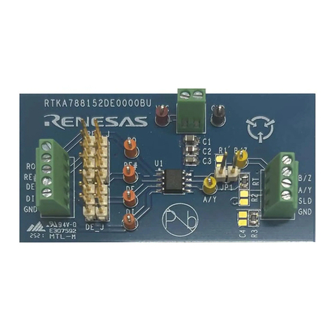
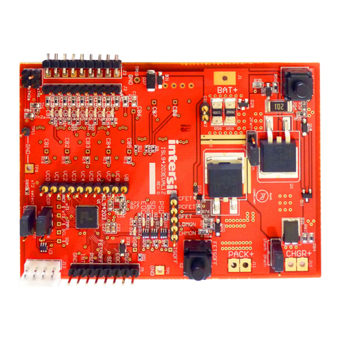
The ZL2102DEMO1Z Demonstration Board is shown in Figure 2
and Figure 3. The hardware enable function is controlled by a
toggle switch. The power-good (PG) LED indicates that VOUT is
regulating. The right angle headers at opposite ends of the board
are for connecting a USB to SMBus control board or for daisy
chaining of multiple Intersil evaluation boards.
Connecting multiple Intersil Zilker Lab boards allows the user to
setup many shared features such as clock synchronization,
controlled sequencing, phase spreading, and fault spreading
within Intersil’s Power Navigator software as part of a single
power project. The ZL2102DEMO1Z Circuit Schematic (Figure 9)
shows the schematic, bill of materials, and PCB layers for
reference. Figures 10 through 13 show performance data taken
using this hardware in its optimized configuration. The
configuration settings that the hardware ships with are shown on
Page 11.
Operating Range
By default, the ZL2102DEMO1Z is configured for the operating
conditions shown in “USB (PMBus) Operation”. The board can
also support a wider operating range, and modifying the
operating conditions will change the performance results.
The board VIN range is 7.5V to 14V. The board VOUT setting is
fixed at 3.3V by pin strap setting, but the programmable range is
0.54V to 3.6V (including margin high/low). The output voltage
can be changed by using the VOUT_COMMAND PMBus
command. The board IOUT range is 0 to 6A. For continuous
operation at 6A, airflow across the board may be needed.
The switching frequency (fSW) is set to 600kHz by PMBus
command, but the fSW setting can be changed by using the
FREQUENCY_SWITCH PMBus command (while the device is
disabled). The fSW range is 200kHz to 1MHz.
PCB Layout Notes
The ZL2102DEMO1Z PCB layout has been optimized for
electrical and thermal performance.
The following key features are:
• The large 5x5 via pattern under the ZL2102 is connected to a
large copper plane for effective thermal dissipation.
• SGND and power GND are isolated. The ZL2102’s thermal pad
is connected to the isolated SGND plane which is then
reconnected to the power GND plane at pin 14 of ZL2102 on
inner layer 1.
• The VSEN pin is Kelvin connected to C2 through inner layer 2
for improved noise performance.
Quick Start Guide
Stand Alone Operation
1. Ensure that the board is properly connected to the supply and
loads prior to applying any power.
2. Connect the input supply to VIN and GND.
3. Connect the load to VOUT and GND.
4. Set ENABLE switch to “DISABLE”.
5. Turn input power supply ON.
6. Set ENABLE switch to “ENABLE”.
7. Test ZL2102 operation.
USB (PMBus) Operation
1. Follow step 1 through 5 of Stand Alone Operation.
2. Download PowerNavigator software from the Intersil website
and install.
3. Connect USB-to-SMBus interface board to J2 of
ZL2102DEMO1Z.
4. Set voltage to desired value in GUI.
5. Set ENABLE switch on EVB to “ENABLE”.
6. Monitor and configure EVB using PMBus commands in the
evaluation software.
7. Test ZL2102 operation using the evaluation software.
