Richtek RT7297B User manual

RT7297B
®
DS7297B-02 September 2012 www.richtek.com
1
©
Copyright 2012 Richtek Technology Corporation. All rights reserved. is a registered trademark of Richtek Technology Corporation.
Ordering Information
Note :
Richtek products are :
`RoHS compliant and compatible with the current require-
ments of IPC/JEDEC J-STD-020.
`Suitable for use in SnPb or Pb-free soldering processes.
Pin Configurations
(TOPVIEW)
Applications
WirelessAP/Router
Set-Top-Box
Industrial and Commercial Low Power Systems
LCDMonitorsandTVs
GreenElectronics/Appliances
PointofLoadRegulationof High-PerformanceDSPs
SOP-8 (Exposed Pad)
3A, 18V, 1.2MHz Synchronous Step-Down Converter
General Description
TheRT7297Bisahighefficiency,monolithicsynchronous
step-down DC/DC converter that can deliver up to 3A
output current from a 4.5V to 18V input supply. The
RT7297B's current mode architecture and external
compensation allow the transient response to be
optimizedoverawideinputvoltagerangeandloads.Cycle-
by-cyclecurrentlimitprovides protection against shorted
outputs,andsoft-starteliminatesinputcurrentsurgeduring
start-up. The RT7297B also provides under voltage
protection and thermal shutdown protection. The low
current (<3μA) shutdown mode provides output
disconnection, enabling easy power management in
battery-powered systems. The RT7297B is available in
an SOP-8 (Exposed Pad) package.
Features
±±
±±
±1.5% High Accuracy Reference Voltage
4.5V to 18V Input Voltage Range
3A Output Current
Integrated N-MOSFET Switches
Current Mode Control
Fixed Frequency Operation : 1.2MHz
Output Adjustable from 0.8V to 12V
Up to 95% Efficiency
Programmable Soft-Start
Stable with Low ESR Ceramic Output Capacitors
Cycle-by-Cycle Over Current Protection
Input Under Voltage Lockout
Output Under Voltage Protection
Thermal Shutdown Protection
RoHS Compliant and Halogen Free
BOOT
VIN
SW
GND
SS
EN
FB
COMP
GND
2
3
45
6
7
8
9
Package Type
SP : SOP-8 (Exposed Pad-Option 1)
RT7297B
Lead Plating System
Z : ECO (Ecological Element with
Halogen Free and Pb free)
H : UVP Hiccup
L : UVP Latch-Off
Marking Information
RT7297BxZSP : Product Number
x : H or L
YMDNN : Date Code
RT7297Bx
ZSPYMDNN

RT7297B
2DS7297B-02 September 2012www.richtek.com
©
Copyright 2012 Richtek Technology Corporation. All rights reserved. is a registered trademark of Richtek Technology Corporation.
Functional Pin Description
Pin No. Pin Name Pin Function
1 BOOT
Bootstrap for High Side Gate Driver. Connect a 0.1μF or greater ceramic
capacitor from BOOT to SW pins.
2 VIN
Input Supply Voltage, 4.5V to 18V. Must bypass with a suitable large ceramic
capacitor.
3 SW Switch Node. Connect this pin to an external L-C filter.
4,
9 (Exposed Pad) GND Ground. The exposed pad must be soldered to a large PCB and connected to
GND for maximum power dissipation.
5 FB Feedback Input. It is used to regulate the output of the converter to a set value
via an external resistive voltage divider.
6 COMP
Compensation Node. COMP is used to compensate the regulation control
loop. Connect a series RC network from COMP to GND. In some cases, an
additional capacitor from COMP to GND is required.
7 EN
Enable Input Pin. A logic high enables the converter; a logic low forces the IC
into shutdown mode reducing the supply current to less than 3μA. Attach this
pin to VIN with a 100kΩpull up resistor for automatic startup.
8 SS Soft-Start Control Input. SS controls the soft-start period. Connect a capacitor
from SS to GND to set the soft-start period. A 0.1μF capacitor sets the
soft-start period to 13.5ms.
Typical Application Circuit
VOUT (V) R1 (kΩ) R2 (kΩ) RC(kΩ) CC(nF) L (μH) COUT (μF)
8 27 3 51 2.2 10 22 x 2
5 62 11.8 33 2.2 6.8 22 x 2
3.3 75 24 22 2.2 3.6 22 x 2
2.5 25.5 12 16 2.2 3.6 22 x 2
1.5 10.5 12 10 2.2 2 22 x 2
1.2 12 24 8.2 2.2 2 22 x 2
1 3 12 6.8 2.2 2 22 x 2
Table 1. Suggested Components Selection
VIN
EN
GND
BOOT
FB
SW
7
5
2
3
1L
3.6µH
0.1µF
22µF x 2
R1
75k
R2
24k
VOUT
3.3V
10µF x 2
VIN
4.5V to 18V RT7297B
SS
8
CSS
COMP
CC
2.2nF RC
22k
CP
Open
6
4, 9 (Exposed Pad)
CBOOT
CIN
0.1µF
COUT
REN 100k

RT7297B
3
DS7297B-02 September 2012 www.richtek.com
©
Copyright 2012 Richtek Technology Corporation. All rights reserved. is a registered trademark of Richtek Technology Corporation.
Function Block Diagram
+
-
+
-
+
-
UV
Comparator
Oscillator
Foldback
Control
0.4V
Internal
Regulator
+
-
Shutdown
Comparator
Current Sense
Amplifier
BOOT
VIN
GND
SW
FB
EN
COMP
VCC
6µA
Slope Comp
Current
Comparator
+
-EA
0.8V
S
R
Q
Q
SS
+
-
1.2V
Lockout
Comparator
VCC
+
Ω90m
Ω110m
VA
2.5V
VARSENSE
5kΩ

RT7297B
4DS7297B-02 September 2012www.richtek.com
©
Copyright 2012 Richtek Technology Corporation. All rights reserved. is a registered trademark of Richtek Technology Corporation.
Electrical Characteristics
(VIN = 12V, TA= 25°C, unless otherwise specified)
Absolute Maximum Ratings (Note 1)
Supply InputVoltage, VIN ----------------------------------------------------------------------------------------- −0.3V to 20V
Switch Voltage, SW ------------------------------------------------------------------------------------------------ −0.3Vto (VIN + 0.3V)
VBOOT −VSW ---------------------------------------------------------------------------------------------------------- −0.3V to 6V
Other Pins Voltage -------------------------------------------------------------------------------------------------- −0.3V to 20V
Power Dissipation, PD@ TA= 25°C
SOP-8 (Exposed Pad) --------------------------------------------------------------------------------------------- 1.333W
Package Thermal Resistance (Note 2)
SOP-8 (Exposed Pad), θJA ---------------------------------------------------------------------------------------- 75°C/W
SOP-8 (Exposed Pad), θJC --------------------------------------------------------------------------------------- 15°C/W
LeadTemperature(Soldering,10sec.)------------------------------------------------------------------------- 260°C
JunctionTemperature----------------------------------------------------------------------------------------------- 150°C
StorageTemperatureRange -------------------------------------------------------------------------------------- −65°Cto150°C
ESD Susceptibility (Note 3)
HBM(HumanBodyModel)---------------------------------------------------------------------------------------- 2kV
Recommended Operating Conditions (Note 4)
Supply InputVoltage, VIN ----------------------------------------------------------------------------------------- 4.5V to 18V
JunctionTemperatureRange-------------------------------------------------------------------------------------- −40°C to125°C
AmbientTemperatureRange-------------------------------------------------------------------------------------- −40°C to 85°C
Parameter Symbol Test Conditions Min Typ Max Unit
Shutdown Supply Current VEN = 0V -- 0.5 3 μA
Supply Current VEN = 3V, VFB = 0.9V -- 0.8 1.2 mA
Reference Voltage VREF 4.5V ≤ VIN ≤ 18V 0.788 0.8 0.812 V
Error Amplifier
Transconductance GEA ΔIC= ±10μA -- 940 -- μA/V
High Side Switch
On-Resistance RDS(ON)1 -- 110 -- mΩ
Low Side Switch
On-Resistance RDS(ON)2 -- 90 -- mΩ
High Side Switch Leakage
Current V
EN = 0V, VSW = 0V -- 0 10 μA
Upper Switch Current Limit Min. Duty Cycle, VBOOT − VSW = 4.8V -- 5.1 -- A
COMP to Current Sense
Transconductance GCS -- 4.7 -- A/V
Oscillation Frequency fOSC1 1 1.2 1.4 MHz
Short Circuit Oscillation
Frequency fOSC2 V
FB = 0V -- 270 -- kHz
Maximum Duty Cycle DMAX V
FB = 0.7V -- 78 -- %
Minimum On Time tON -- 100 -- ns

RT7297B
5
DS7297B-02 September 2012 www.richtek.com
©
Copyright 2012 Richtek Technology Corporation. All rights reserved. is a registered trademark of Richtek Technology Corporation.
Parameter Symbol Test Conditions Min Typ Max Unit
Logic-High VIH 2.7 -- 18
EN Input Threshold
Voltage Logic-Low VIL -- -- 0.4
V
Input Under Voltage Lockout
Threshold VUVLO V
IN Rising 3.8 4.2 4.5 V
Input Under Voltage Lockout
Hysteresis ΔVUVLO -- 320 -- mV
Soft-Start Current ISS V
SS = 0V -- 6 -- μA
Soft-Start Period tSS C
SS = 0.1μF -- 13.5 -- ms
Thermal Shutdown TSD -- 150 -- °C
Note 1. Stresses beyond those listed “Absolute Maximum Ratings”may cause permanent damage to the device. These are
stress ratings only, and functional operation of the device at these or any other conditions beyond those indicated in
the operational sections of the specifications is not implied. Exposure to absolute maximum rating conditions may
affect device reliability.
Note 2. θJA is measured at TA= 25°C on a high effective thermal conductivity four-layer test board per JEDEC 51-7. θJC is
measured at the exposed pad of the package.
Note 3. Devices are ESD sensitive. Handling precaution is recommended.
Note 4. The device is not guaranteed to function outside its operating conditions.

RT7297B
6DS7297B-02 September 2012www.richtek.com
©
Copyright 2012 Richtek Technology Corporation. All rights reserved. is a registered trademark of Richtek Technology Corporation.
Typical Operating Characteristics
Efficiency vs. Load Current
0
10
20
30
40
50
60
70
80
90
100
00.511.522.53
Load Current (A)
Efficiency (%)
VOUT = 3.3V
VIN = 12V
VIN = 17V
Output Voltage vs. Temperature
3.26
3.27
3.28
3.29
3.30
3.31
3.32
3.33
3.34
-50 -25 0 25 50 75 100 125
Temperature (°C)
Output Voltage (V)
VIN = 12V, VOUT = 3.3V
Output Voltage vs. Load Current
3.20
3.22
3.24
3.26
3.28
3.30
3.32
3.34
3.36
3.38
3.40
0 0.5 1 1.5 2 2.5 3
Load Current (A)
Output Voltage (V)
VOUT = 3.3V
VIN = 12V
VIN = 17V
Switching Frequency vs. Temperature
1.10
1.11
1.12
1.13
1.14
1.15
1.16
1.17
1.18
1.19
1.20
1.21
1.22
1.23
1.24
-50 -25 0 25 50 75 100 125
Temperature (°C)
Switching Frequency (kHz)1
VOUT = 3.3V, IOUT = 0A
VIN = 17V
VIN = 12V
Switching Frequency vs. Input Voltage
1.16
1.17
1.18
1.19
1.20
1.21
1.22
1.23
1.24
1.25
1.26
4.5 7 9.5 12 14.5 17
Input Voltage (V)
Switching Frequency (MHz)1
VIN = 4.5V to 17V, VOUT = 3.3V, IOUT = 0A
Output Voltage vs. Input Voltage
3.26
3.27
3.28
3.29
3.30
3.31
3.32
3.33
3.34
4 6 8 1012141618
Input Voltage (V)
Output Voltage (V)
VIN = 4.5V to 17V

RT7297B
7
DS7297B-02 September 2012 www.richtek.com
©
Copyright 2012 Richtek Technology Corporation. All rights reserved. is a registered trademark of Richtek Technology Corporation.
Current Limit vs. Temperature
3.0
3.5
4.0
4.5
5.0
5.5
6.0
6.5
7.0
-50-25 0 25 50 75100125
Temperature (°C)
Current Limit (A)
VIN = 12V, VOUT = 3.3V
Current Limit vs. Input Voltage
1.0
1.5
2.0
2.5
3.0
3.5
4.0
4.5
5.0
5.5
6.0
4.5 7 9.5 12 14.5 17
Input Voltage (V)
Current Limit (A)
VIN = 4.5V to 17V, VOUT = 3.3V
Time (100μs/Div)
Load Transient Response
VOUT
(100mV/Div)
IOUT
(2A/Div)
VIN = 12V, VOUT = 3.3V, IOUT = 0A to 3A
Time (100μs/Div)
Load Transient Response
VOUT
(100mV/Div)
IOUT
(2A/Div)
VIN = 12V, VOUT = 3.3V, IOUT = 1.5A to 3A
Time (500ns/Div)
Switching
VSW
(10V/Div)
VOUT
(5mV/Div)
IL
(2A/Div) VIN = 12V, VOUT = 3.3V, IOUT = 1.5A
Time (500ns/Div)
Switching
VIN = 12V, VOUT = 3.3V, IOUT = 3A
VSW
(10V/Div)
VOUT
(5mV/Div)
IL
(2A/Div)

RT7297B
8DS7297B-02 September 2012www.richtek.com
©
Copyright 2012 Richtek Technology Corporation. All rights reserved. is a registered trademark of Richtek Technology Corporation.
Power On from VIN
Time (10ms/Div)
VIN = 12V, VOUT = 3.3V, IOUT = 3A
IL
(2A/Div)
VOUT
(2V/Div)
VIN
(5V/Div)
Power Off from VIN
Time (10ms/Div)
IL
(2A/Div)
VOUT
(2V/Div)
VIN
(5V/Div)
VIN = 12V, VOUT = 3.3V, IOUT = 3A
Power On from EN
Time (10ms/Div)
VOUT
(2V/Div)
VEN
(5V/Div)
IL
(2A/Div) VIN = 12V, VOUT = 3.3V, IOUT = 3A
Power Off from EN
Time (10ms/Div)
VIN = 12V, VOUT = 3.3V, IOUT = 3A
VOUT
(2V/Div)
VEN
(5V/Div)
IL
(2A/Div)

RT7297B
9
DS7297B-02 September 2012 www.richtek.com
©
Copyright 2012 Richtek Technology Corporation. All rights reserved. is a registered trademark of Richtek Technology Corporation.
Application Information
Output Voltage Setting
TheresistivedividerallowstheFBpin to sense the output
voltage as shown in Figure 1.
Figure 1. Output Voltage Setting
The output voltage is set by an external resistive voltage
divideraccordingto the followingequation:
OUT REF R1
V =V 1
R2
⎛⎞
+
⎜⎟
⎝⎠
Where VREF is the reference voltage (0.8V typ.).
External Bootstrap Diode
Connect a 100nF low ESR ceramic capacitor between
the BOOT pin and SW pin. This capacitor provides the
gatedrivervoltage forthehighsideMOSFET.
It is recommended to add an external bootstrap diode
between an external 5V and BOOT pin for efficiency
improvementwheninputvoltageislowerthan5.5Vorduty
ratio is higher than 65% .The bootstrap diode can be a
low cost one such as IN4148 or BAT54. The external 5V
can be a 5V fixed input from system or a 5V output of the
RT7297B. Note that the external boot voltage must be
lowerthan 5.5V
Figure 2. External BootstrapDiode
Chip Enable Operation
The EN pin is the chip enable input. Pulling the EN pin
low (<0.4V) will shutdown the device. During shutdown
mode,theRT7297B quiescentcurrentdropstolower than
3μA. Driving the EN pin high (>2.7V, <18V) will turn on
the device again. For external timing control, the EN pin
canalsobeexternallypulled highbyaddingaREN resistor
and CEN capacitor from the VINpin (see Figure 3).
SW
BOOT
5V
RT7297B 0.1µF
RT7297B
GND
FB
R1
R2
VOUT
Soft-Start
The RT7297B provides soft-start function. The soft-start
function is used to prevent large inrush current while
converter is being powered-up. The soft-start timing can
beprogrammedbytheexternalcapacitorbetweenSS and
GND. An internal current source ISS (6μA) charges an
external capacitor to build a soft-start ramp voltage. The
VFB voltagewilltrackthe internalramp voltage duringsoft-
start interval. The typical soft-start time is calculated as
follows :
RT7297B
EN
GND
VIN REN
CEN
EN
An external MOSFET can be added to implement digital
controlontheENpin when nosystemvoltageabove1.8V
is available, as shown in Figure 4. In this case, a 100kΩ
pull-up resistor, REN, is connected between VIN and the
EN pin. MOSFET Q1 will be under logic control to pull
down the EN pin.
RT7297B
EN
GND
100k
VIN
REN
Q1
EN
Figure3.EnableTimingControl
Figure 4.Digital Enable Control Circuit
SS
SS SS
SS
0.8 C
Soft-Start time t = , if C capacitor
I0.8 0.1
is 0.1 F, then soft-start time = 13.5ms
6
μ
μμ
×
× ≒

RT7297B
10 DS7297B-02 September 2012www.richtek.com
©
Copyright 2012 Richtek Technology Corporation. All rights reserved. is a registered trademark of Richtek Technology Corporation.
OUT OUT
LIN
VV
I = 1
fL V
⎡⎤⎡ ⎤
Δ×−
⎢⎥⎢ ⎥
×
⎣⎦⎣ ⎦
Under Voltage Protection
Hiccup Mode
FortheRT7297BH,itprovidesHiccupMode UnderVoltage
Protection (UVP). When the VFB voltage drops below
0.4V, the UVP function will be triggered to shut down
switching operation. If the UVP condition remains for a
period, the RT7297BH will retry automatically. When the
UVP condition is removed, the converter will resume
operation. The UVP is disabled during Soft-Start period.
Having a lower ripple current reduces not only the ESR
lossesintheoutputcapacitors butalsotheoutputvoltage
ripple.Highfrequencywithsmall ripplecurrent canachieve
the highest efficiency operation. However, it requires a
large inductor to achieve this goal.
Fortheripplecurrentselection,the valueofΔIL=0.24(IMAX)
will be a reasonable starting point. The largest ripple
current occurs at the highest VIN. To guarantee that the
ripple current stays below the specified maximum, the
inductorvalueshould bechosenaccordingto thefollowing
equation :
Table 2. Suggested Inductors for Typical
Application Circuit
Component
Supplier Series Dimensions
(mm)
TDK VLF10045 10 x 9.7 x 4.5
TDK SLF12565 12.5 x 12.5x 6.5
TAIYO
YUDEN NR8040 8 x 8 x 4
OUT OUT
L(MAX) IN(MAX)
VV
L = 1
fI V
⎡⎤⎡ ⎤
×−
⎢⎥⎢ ⎥
×Δ
⎣⎦⎣ ⎦
Theinductor'scurrentrating(causeda40°Ctemperature
rising from 25°C ambient) should be greater than the
maximum load current and its saturation current should
begreaterthanthe short circuit peak current limit.Please
see Table 2 for the inductor selection reference.
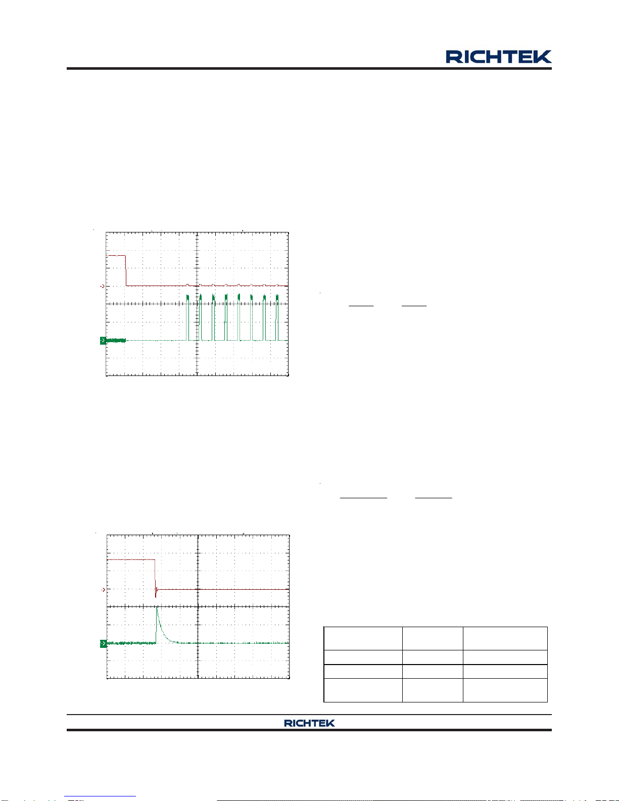
Figure 5. Hiccup Mode Under Voltage Protection
Figure6.Latch-OffModeUnderVoltageProtection
Latch-Off Mode
For the RT7297BL, it provides Latch-Off Mode Under
Voltage Protection (UVP). When the FB voltage drops
below half of the feedback reference voltage, VFB, UVP
willbetriggered andtheRT7297BLwillshutdownin Latch-
Off Mode. In shutdown condition, the RT7297BL can be
reset by EN pin or power input VIN.
Over Temperature Protection
The RT7297B features an Over Temperature Protection
(OTP) circuitry to prevent from overheating due to
excessive power dissipation. The OTP will shut down
switching operation when junction temperature exceeds
150°C. Once the junction temperature cools down by
approximately20°C,theconverterwillresumeoperation.
Tomaintaincontinuousoperation,themaximumjunction
temperatureshouldbelowerthan125°C.
Inductor Selection
Theinductorvalueandoperating frequencydeterminethe
ripple current according to a specific input and output
voltage. The ripple current ΔILincreases with higher VIN
anddecreases with higher inductance.
Time (50ms/Div)
Hiccup Mode
VOUT
(2V/Div)
ILX
(2A/Div)
IOUT = Short
Time (250μs/Div)
Latch-Off Mode
VOUT
(2V/Div)
ILX
(2A/Div)
IOUT = Short

RT7297B
11
DS7297B-02 September 2012 www.richtek.com
©
Copyright 2012 Richtek Technology Corporation. All rights reserved. is a registered trademark of Richtek Technology Corporation.
OUT IN
RMS OUT(MAX) IN OUT
VV
I =I 1
VV
−
CIN and COUT Selection
The input capacitance, CIN, is needed to filter the
trapezoidalcurrentatthesourceofthehighsideMOSFET.
Topreventlargeripplecurrent, alowESRinputcapacitor
sizedforthemaximumRMScurrentshouldbeused.The
approximate RMS current is given :
This formula has a maximum at VIN = 2VOUT, where
IRMS = IOUT / 2. This simple worst case condition is
commonly used for design because even significant
deviations do not offer much relief. Choose a capacitor
rated at a higher temperature than required. Several
capacitors may also be paralleled to meet size or height
requirements in the design. For the input capacitor, two
10μFlowESRceramic capacitorsaresuggested.Forthe
suggested
capacitor, please refer to Table 3 for more details. The
selection of COUT is determined by the required ESR to
minimize voltage ripple. Moreover, the amount of bulk
capacitance is also a key for COUT selection to ensure
that the control loop is stable. Loop stability can be
checked by viewing the load transient response as
described in a later section.
The output ripple, ΔVOUT, is determined by :
OUT L OUT
1
VIESR
8fC
⎡⎤
Δ≤Δ +
⎢⎥
⎣⎦
Theoutputripplewillbethehighest at the maximum input
voltage since ΔILincreases with input voltage. Multiple
capacitors placed in parallel may be needed to meet the
ESRandRMScurrenthandlingrequirement.Highervalues,
lowercostceramiccapacitorsarenowbecomingavailable
insmallercasesizes.Theirhighripplecurrent,highvoltage
ratingandlow ESRmakethemidealforswitchingregulator
applications. However, care must be taken when these
capacitors are used at input and output. When a ceramic
capacitor is used at the input and the power is supplied
by a wall adapter through long wires, a load step at the
output can induce ringing at the input, VIN. At best, this
ringing can couple to the output and be mistaken as loop
instability. At worst, a sudden inrush of current through
the long wires can potentially cause a voltage spike at
VIN large enough to damage the part.
Thermal Considerations
For continuous operation, do not exceed the maximum
operation junction temperature 125°C. The maximum
power dissipation depends on the thermal resistance of
IC package, PCB layout, the rate of surroundings airflow
andtemperature differencebetweenjunctiontoambient.
The maximum power dissipation can be calculated by
followingformula:
PD(MAX) = (TJ(MAX) − TA ) / θJA
Where TJ(MAX) is the maximum operation junction
temperature,TAis theambient temperatureandthe θJAis
the junction to ambient thermal resistance.
For recommended operating conditions specification of
RT7297B, the maximum junction temperature is 125°C.
The junction to ambient thermal resistance θJA is layout
dependent. For SOP-8 (Exposed Pad) package, the
thermalresistance θJA is75°C/WonthestandardJEDEC
51-7four-layersthermaltestboard.Themaximumpower
dissipation at TA= 25°C can be calculated by following
formula :
PD(MAX) = (125°C −25°C) / (75°C/W) = 1.333W
(min.copper area PCB layout)
PD(MAX) = (125°C −25°C) / (49°C/W) = 2.04W
(70mm2copperareaPCBlayout)
The thermal resistance θJA of SOP-8 (Exposed Pad) is
determined by the package architecture design and the
PCB layout design. However, the package architecture
design had been designed. If possible, it's useful to
increase thermal performance by the PCB layout copper
design. The thermal resistance θJA can be decreased by
adding copper area under the exposed pad of SOP-8
(ExposedPad)package.
AsshowninFigure7,theamountofcopperareatowhich
the SOP-8 (Exposed Pad) is mounted affects thermal
performance. When mounted to the standard
SOP-8 (Exposed Pad) pad (Figure 7.a), θJA is 75°C/W.
Adding copper area of pad under the SOP-8 (Exposed
Pad) (Figure7.b)reducestheθJA to64°C/W.Evenfurther,
increasing the copper area of pad to 70mm2(Figure 7.e)
reduces the θJA to 49°C/W.

RT7297B
12 DS7297B-02 September 2012www.richtek.com
©
Copyright 2012 Richtek Technology Corporation. All rights reserved. is a registered trademark of Richtek Technology Corporation.
(d) CopperArea = 50mm2,θJA = 51°C/W
(e) CopperArea = 70mm2,θJA = 49°C/W
Figure7.ThermalResistancevs.CopperArea Layout
Design
Figure8.DeratingCurveofMaximumPowerDissipation
(a) Copper Area = (2.3 x 2.3) mm2,θJA = 75°C/W
(b) CopperArea = 10mm2,θJA = 64°C/W
(c) Copper Area = 30mm2,θJA = 54°C/W
0.0
0.2
0.4
0.6
0.8
1.0
1.2
1.4
1.6
1.8
2.0
2.2
0 25 50 75 100 125
Ambient Temperature (°C)
Power Dissipation (W)
Copper Area
70mm2
50mm2
30mm2
10mm2
Min.Layout
Four-Layer PCB
Themaximumpowerdissipationdependsontheoperating
ambient temperature for fixed TJ(MAX) and thermal
resistance, θJA.ThederatingcurveinFigure8ofderating
curves allows the designer to see the effect of rising
ambient temperature on the maximum power dissipation
allowed.

RT7297B
13
DS7297B-02 September 2012 www.richtek.com
©
Copyright 2012 Richtek Technology Corporation. All rights reserved. is a registered trademark of Richtek Technology Corporation.
Layout Consideration
FollowthePCBlayoutguidelinesforoptimalperformance
oftheRT7297B.
`Keep the traces of the main current paths as short and
wide as possible.
`Puttheinputcapacitorascloseaspossibletothedevice
pins(VINandGND).
Figure 9. PCB LayoutGuide
Table 3. Suggested Capacitors for CIN and COUT
Location Component Supplier Part No. Capacitance (μF) Case Size
CIN MURATA GRM31CR61E106K 10 1206
CIN TDK C3225X5R1E106K 10 1206
CIN TAIYO YUDEN TMK316BJ106ML 10 1206
COUT MURATA GRM31CR60J476M 47 1206
COUT TDK C3225X5R0J476M 47 1210
COUT MURATA GRM32ER71C226M 22 1210
COUT TDK C3225X5R1C22M 22 1210
`SW node is with high frequency voltage swing and
shouldbekeptatsmallarea.Keepanalogcomponents
away from the SW node to prevent stray capacitive
noise pick-up.
`Connectfeedbacknetworkbehindtheoutputcapacitors.
Keep the loop area small. Place the feedback
components nearthe RT7297B.
`An example of PCB layout guide is shown in Figure 9
forreference.
VIN
VOUT
GND
CIN
GND
CP
CC
RC
SW
VOUT
COUT
L
R1
R2
Input capacitor must
be placed as close
to the IC as possible.
SW nods is with high frequency voltage swing and should
be kept at small area. Keep analog components away from
the SW node to prevent stray capacitive noise pick-up
The feedback components
must be connected as close
to the device as possible.
BOOT
VIN
SW
GND
SS
EN
FB
COMP
GND
2
3
45
6
7
8
9
CSS
GND VIN
REN
CBOOT

RT7297B
14 DS7297B-02 September 2012www.richtek.com
Richtek Technology Corporation
5F, No. 20, Taiyuen Street, Chupei City
Hsinchu, Taiwan, R.O.C.
Tel: (8863)5526789
Richtek products are sold by description only. Richtek reserves the right to change the circuitry and/or specifications without notice at any time. Customers should
obtain the latest relevant information and data sheets before placing orders and should verify that such information is current and complete. Richtek cannot
assume responsibility for use of any circuitry other than circuitry entirely embodied in a Richtek product. Information furnished by Richtek is believed to be
accurate and reliable. However, no responsibility is assumed by Richtek or its subsidiaries for its use; nor for any infringements of patents or other rights of third
parties which may result from its use. No license is granted by implication or otherwise under any patent or patent rights of Richtek or its subsidiaries.
Outline Dimension
A
B
J
F
H
M
C
D
I
Y
X
EXPOSED THERMAL PAD
(Bottom of Package)
8-Lead SOP (Exposed Pad) Plastic Package
Dimensions In Millimeters Dimensions In Inches
Symbol Min Max Min Max
A 4.801 5.004 0.189 0.197
B 3.810 4.000 0.150 0.157
C 1.346 1.753 0.053 0.069
D 0.330 0.510 0.013 0.020
F 1.194 1.346 0.047 0.053
H 0.170 0.254 0.007 0.010
I 0.000 0.152 0.000 0.006
J 5.791 6.200 0.228 0.244
M 0.406 1.270 0.016 0.050
X 2.000 2.300 0.079 0.091
Option 1 Y 2.000 2.300 0.079 0.091
X 2.100 2.500 0.083 0.098
Option 2 Y 3.000 3.500 0.118 0.138
Table of contents
Other Richtek Media Converter manuals