Richtek RT7247A User manual

RT7247A
®
DS7247A-03 October 2016 www.richtek.com
1
Copyright 2016 Richtek Technology Corporation. All rights reserved. is a registered trademark of Richtek Technology Corporation.
©
Design
Tools Sample &
Buy
Applications
WirelessAP/Router
Set-Top-Box
Industrial and Commercial Low Power Systems
LCDMonitorsandTVs
GreenElectronics/Appliances
PointofLoadRegulationof High-PerformanceDSPs
2A, 18V, 340kHz Synchronous Step-Down Converter
General Description
TheRT7247Aisahighefficiency,monolithicsynchronous
step-down DC/DC converter that can deliver up to 2A
output current from a 4.5V to 18V input supply. The
RT7247A's current mode architecture and external
compensation allow the transient response to be
optimized over a wide input range and loads. Cycle-by-
cycle current limit provides protection against shorted
outputs,and soft-starteliminatesinputcurrentsurgeduring
start-up. The RT7247A also provides under voltage
protection and thermal shutdown protection. The low
current (<3μA) shutdown mode provides output
disconnection, enabling easy power management in
battery-powered systems. The RT7247A is available in
an SOP-8 (Exposed Pad) package.
Features
±±
±±
±1.5% High Accuracy Reference Voltage
4.5V to 18V Input Voltage Range
2A Output Current
Integrated N-MOSFET Switches
Current Mode Control
Fixed Frequency Operation : 340kHz
Output Adjustable from 0.8V to 15V
Stable with Low ESR Ceramic Output Capacitors
Up to 95% Efficiency
Programmable Soft-Start
Cycle-by-Cycle Over Current Protection
Input Under Voltage Lockout
Output Under Voltage Protection
Thermal Shutdown Protection
RoHS Compliant and Halogen Free
Marking Information
RT7247Ax
GSPYMDNN
RT7247AxGSP : Product Number
x : H or L or N
YMDNN : Date Code
Simplified Application Circuit
VIN
EN
GND
BOOT
FB
SW L
R1
R2
VOUT
VIN RT7247A
SS
CSS COMP CCRC
CP
CBOOT
CIN
COUT
Chip Enable

RT7247A
2DS7247A-03 October 2016www.richtek.com
©
Copyright 2016 Richtek Technology Corporation. All rights reserved. is a registered trademark of Richtek Technology Corporation.
Functional Pin Description
Pin No. Pin Name Pin Function
1 BOOT
Bootstrap for High Side Gate Driver. Connect a 0.1F or greater ceramic
capacitor from BOOT to SW pins.
2 VIN
Input Supply Voltage, 4.5V to 18V. Must bypass with a suitable large ceramic
capacitor.
3 SW Switch Node. Connect this pin to an external L-C filter.
4,
9 (Exposed Pad) GND Ground. The exposed pad must be soldered to a large PCB and connected to
GND for maximum power dissipation.
5 FB Feedback Input. It is used to regulate the output of the converter to a set value
via an external resistive voltage divider.
6 COMP
Compensation Node. COMP is used to compensate the regulation control
loop. Connect a series RC network from COMP to GND. In some cases, an
additional capacitor from COMP to GND is required.
7 EN
Enable Input. A logic high enables the converter; a logic low forces the IC into
shutdown mode reducing the supply current to less than 3A. Attach this pin
to VIN with a 100kpull-up resistor for automatic startup.
8 SS Soft-Start Control Input. SS controls the soft-start period. Connect a capacitor
from SS to GND to set the soft-start period. A 0.1F capacitor sets the
soft-start period to 13.5ms.
Ordering Information
Note :
Richtek products are :
RoHS compliant and compatible with the current require-
ments of IPC/JEDEC J-STD-020.
Suitable for use in SnPb or Pb-free soldering processes.
Package Type
SP : SOP-8 (Exposed Pad-Option 2)
RT7247A
Lead Plating System
G : Green (Halogen Free and Pb Free)
H : UVP Hiccup
L : UVP Latch-Off
N : UVP Disabled
Pin Configurations
(TOPVIEW)
SOP-8 (Exposed Pad)
BOOT
VIN
SW
GND
SS
EN
FB
COMP
GND
2
3
45
6
7
8
9

RT7247A
3
DS7247A-03 October 2016 www.richtek.com
©
Copyright 2016 Richtek Technology Corporation. All rights reserved. is a registered trademark of Richtek Technology Corporation.
Function Block Diagram
RSENSE
+
-
+
-
+
-
UV
Comparator
Oscillator
Foldback
Control
0.4V
Internal
Regulator
+
-
1.8V
Shutdown
Comparator
Current Sense
Amplifier
BOOT
VIN
GND
SW
FB
EN
COMP
VAVCC
6µA
Slope Comp
Current
Comparator
+
-EA
0.8V
S
R
Q
Q
SS
+
-
1.2V
Lockout
Comparator
VCC
+
150m
5k
VA
130m
Operation
Shutdown Comparator
Activate internal regulator once EN input level is larger
than the target level. Force IC to enter shutdown mode
when the ENinput level is lower than 0.4V.
Internal Regulator
Provide internal power for logic control and switch gate
drivers.
Lockout Comparator
Activate the Current Comparator, release lock-out logic,
and enable the switches as EN input level is larger than
lockout voltage. Otherwise, the switches still locks out.
Oscillator
The oscillator provides internal clock and controls the
converter'sswitchingfrequency.
Foldback Control
Dynamicallyadjusttheinternal clock. It provides a slower
frequency as a lower FB voltage.
UV Comparator
AsFBvoltageis lower than the UVvoltage,it will activate
a UV protect scheme.
ErrorAmp
TheoutputvoltageCOMPoftheerroramplifieris adjusted
comparing FB signal with the internal reference voltage
and SS signal.
Current Sense Amplifier
RSENSE detects the peak current of the high-side switch.
This signal is amplified by the Current Sense Amplifier
and added with a Slope Compensation. Then, it controls
the switches by comparing this signal with the COMP
voltage.

RT7247A
4DS7247A-03 October 2016www.richtek.com
©
Copyright 2016 Richtek Technology Corporation. All rights reserved. is a registered trademark of Richtek Technology Corporation.
Electrical Characteristics
(VIN = 12V, TA= 25°C, unless otherwise specified)
Absolute Maximum Ratings (Note 1)
Supply Input Voltage, VIN ------------------------------------------------------------------------------------------ −0.3V to 20V
Switch Voltage, SW ------------------------------------------------------------------------------------------------ −0.3V to (VIN + 0.3V)
<10ns ------------------------------------------------------------------------------------------------------------------ −5V to 25V
VBOOT −VSW ---------------------------------------------------------------------------------------------------------- −0.3V to 6V
Other Pins Voltage ------------------------------------------------------------------------------------------------- −0.3V to 20V
Power Dissipation, PD@ TA= 25°C
SOP-8 (Exposed Pad) --------------------------------------------------------------------------------------------- 1.333W
PackageThermal Resistance (Note 2)
SOP-8 (Exposed Pad), θJA ---------------------------------------------------------------------------------------- 75°C/W
SOP-8 (Exposed Pad), θJC --------------------------------------------------------------------------------------- 15°C/W
LeadTemperature(Soldering,10sec.)------------------------------------------------------------------------- 260°C
JunctionTemperature----------------------------------------------------------------------------------------------- 150°C
StorageTemperatureRange -------------------------------------------------------------------------------------- −65°Cto150°C
ESD Susceptibility (Note 3)
HBM(HumanBodyModel)---------------------------------------------------------------------------------------- 2kV
Recommended Operating Conditions (Note 4)
Supply Input Voltage, VIN ------------------------------------------------------------------------------------------ 4.5V to 18V
JunctionTemperatureRange-------------------------------------------------------------------------------------- −40°Cto 125°C
AmbientTemperatureRange-------------------------------------------------------------------------------------- −40°Cto85°C
Parameter Symbol Test Conditions Min Typ Max Unit
Shutdown Supply Current VEN = 0V -- 0.5 3 A
Supply Current VEN = 3V, VFB = 0.9V -- 0.8 1.2 mA
Reference Voltage VREF 4.5V VIN 18V 0.788 0.8 0.812 V
Error Amplifier
Transconductance GEA IC= ±10A -- 940 -- A/V
High Side Switch
On-Resistance RDS(ON)1 -- 150 -- m
Low Side Switch
On-Resistance RDS(ON)2 -- 130 -- m
High Side Switch Leakage
Current V
EN = 0V, VSW = 0V -- 0 10 A
Upper Switch Current Limit Min. Duty Cycle, VBOOT VSW = 4.8V -- 4 -- A
COMP to Current Sense
Transconductance GCS -- 3.7 -- A/V
Oscillation Frequency fOSC1 300 340 380 kHz
Short Circuit Oscillation
Frequency fOSC2 V
FB = 0V -- 100 -- kHz
Maximum Duty Cycle DMAX V
FB = 0.7V -- 93 -- %
Minimum On-Time tON -- 100 -- ns

RT7247A
5
DS7247A-03 October 2016 www.richtek.com
©
Copyright 2016 Richtek Technology Corporation. All rights reserved. is a registered trademark of Richtek Technology Corporation.
Parameter Symbol Test Conditions Min Typ Max Unit
Logic-High VIH 2 -- 18
EN Input Voltage Logic-Low VIL -- -- 0.4
V
Input Under Voltage Lockout
Threshold VUVLO V
IN Rising 3.8 4.2 4.5 V
Input Under Voltage Lockout
Hysteresis VUVLO -- 320 -- mV
Soft-Start Current ISS V
SS = 0V -- 6 -- A
Soft-Start Period tSS C
SS = 0.1F -- 13.5 -- ms
Thermal Shutdown TSD -- 150 -- C
Note 1. Stresses beyond those listed “Absolute Maximum Ratings”may cause permanent damage to the device. These are
stress ratings only, and functional operation of the device at these or any other conditions beyond those indicated in
the operational sections of the specifications is not implied. Exposure to absolute maximum rating conditions may
affect device reliability.
Note 2. θJA is measured at TA= 25°C on a high effective thermal conductivity four-layer test board per JEDEC 51-7. θJC is
measured at the exposed pad of the package.
Note 3. Devices are ESD sensitive. Handling precaution is recommended.
Note 4. The device is not guaranteed to function outside its operating conditions.

RT7247A
6DS7247A-03 October 2016www.richtek.com
©
Copyright 2016 Richtek Technology Corporation. All rights reserved. is a registered trademark of Richtek Technology Corporation.
Typical Application Circuit
VOUT (V) R1 (k) R2 (k) RC(k) CC(nF) L (H) COUT (F)
8 27 3 27 3.3 22 22 x 2
5 62 11.8 20 3.3 15 22 x 2
3.3 75 24 13 3.3 10 22 x 2
2.5 25.5 12 9.1 3.3 6.8 22 x 2
1.5 10.5 12 4.7 3.3 3.6 22 x 2
1.2 12 24 3.6 3.3 3.6 22 x 2
1 3 12 3 3.3 3.6 22 x 2
Table 1. Suggested Components Selection
VIN
EN
GND
BOOT
FB
SW
7
5
2
3
1L
10µH
0.1µF
22µF x 2
R1
75k
R2
24k
VOUT
3.3V
10µF x 2
VIN
4.5V to 18V RT7247A
SS
8
CSS
COMP
CC
3.3nF RC
13k
CP
Open
6
4, 9 (Exposed Pad)
CBOOT
CIN
0.1µF
COUT
Chip Enable

RT7247A
7
DS7247A-03 October 2016 www.richtek.com
©
Copyright 2016 Richtek Technology Corporation. All rights reserved. is a registered trademark of Richtek Technology Corporation.
Typical Operating Characteristics
Efficiency vs. Output Current
0
10
20
30
40
50
60
70
80
90
100
0 0.25 0.5 0.75 1 1.25 1.5 1.75 2
Output Current (A)
Efficiency (%)
VOUT = 3.3V
VIN = 4.5V
VIN = 12V
VIN = 17V
Output Voltage vs. Input Voltage
3.27
3.28
3.29
3.30
3.31
3.32
3.33
4 6 8 1012141618
Input Voltage (V)
Output Voltage (V)
VOUT = 3.3V, IOUT = 1A
Reference Voltage vs. Temperature
0.75
0.76
0.77
0.78
0.79
0.80
0.81
0.82
0.83
0.84
0.85
-50-25 0 25 50 75100125
Temperature (°C)
Reference Voltage (V)
VOUT = 3.3V, IOUT = 1A
VIN = 4.5V
VIN = 12V
VIN = 17V
Output Voltage vs. Output Current
3.280
3.285
3.290
3.295
3.300
3.305
3.310
0 0.25 0.5 0.75 1 1.25 1.5 1.75 2
Output Current (A)
Output Voltage (V)
VOUT = 3.3V
VIN = 4.5V
VIN = 12V
VIN = 17V
Switching Frequency vs. Input Voltage
300
310
320
330
340
350
360
370
380
369121518
Input Voltage (V)
Switching Frequency (kHz)1
VOUT = 3.3V, IOUT = 0A
Switching Frequency vs. Temperature
300
310
320
330
340
350
360
370
380
-50-25 0 25 50 75100125
Temperature (°C)
Switching Frequency (kHz)1
VOUT = 3.3V, IOUT = 0A
VIN = 4.5V
VIN = 12V
VIN = 17V

RT7247A
8DS7247A-03 October 2016www.richtek.com
©
Copyright 2016 Richtek Technology Corporation. All rights reserved. is a registered trademark of Richtek Technology Corporation.
Time (10ms/Div)
Power On from VIN
VOUT
(2V/Div)
VIN
(5V/Div)
IL
(2A/Div) VIN = 12V, VOUT = 3.3V, IOUT = 2A
Time (10ms/Div)
Power Off from VIN
VOUT
(2V/Div)
VIN
(5V/Div)
IL
(2A/Div) VIN = 12V, VOUT = 3.3V, IOUT = 2A
Time (2.5μs/Div)
Output Ripple Voltage
VOUT
(5mV/Div)
VSW
(5V/Div)
IL
(1A/Div) VIN = 12V, VOUT = 3.3V, IOUT = 2A
Time (100μs/Div)
Load Transient Response
VOUT
(100mV/Div)
IOUT
(1A/Div) VIN = 12V, VOUT = 3.3V, IOUT = 1A to 2A
Current Limit vs. Temperature
2.0
2.5
3.0
3.5
4.0
4.5
5.0
5.5
6.0
-50-25 0 25 50 75100125
Temperature (°C)
Current Limit (A)
VOUT = 3.3V
VIN = 12V
VIN = 17V
Time (100μs/Div)
Load Transient Response
VOUT
(100mV/Div)
IOUT
(1A/Div) VIN = 12V, VOUT = 3.3V, IOUT = 0A to 2A

RT7247A
9
DS7247A-03 October 2016 www.richtek.com
©
Copyright 2016 Richtek Technology Corporation. All rights reserved. is a registered trademark of Richtek Technology Corporation.
Time (10ms/Div)
Power On from EN
VOUT
(2V/Div)
VEN
(5V/Div)
IL
(1A/Div) VIN = 12V, VOUT = 3.3V, IOUT = 2A
Time (10ms/Div)
Power Off from EN
VOUT
(2V/Div)
VEN
(5V/Div)
IL
(1A/Div) VIN = 12V, VOUT = 3.3V, IOUT = 2A

RT7247A
10 DS7247A-03 October 2016www.richtek.com
©
Copyright 2016 Richtek Technology Corporation. All rights reserved. is a registered trademark of Richtek Technology Corporation.
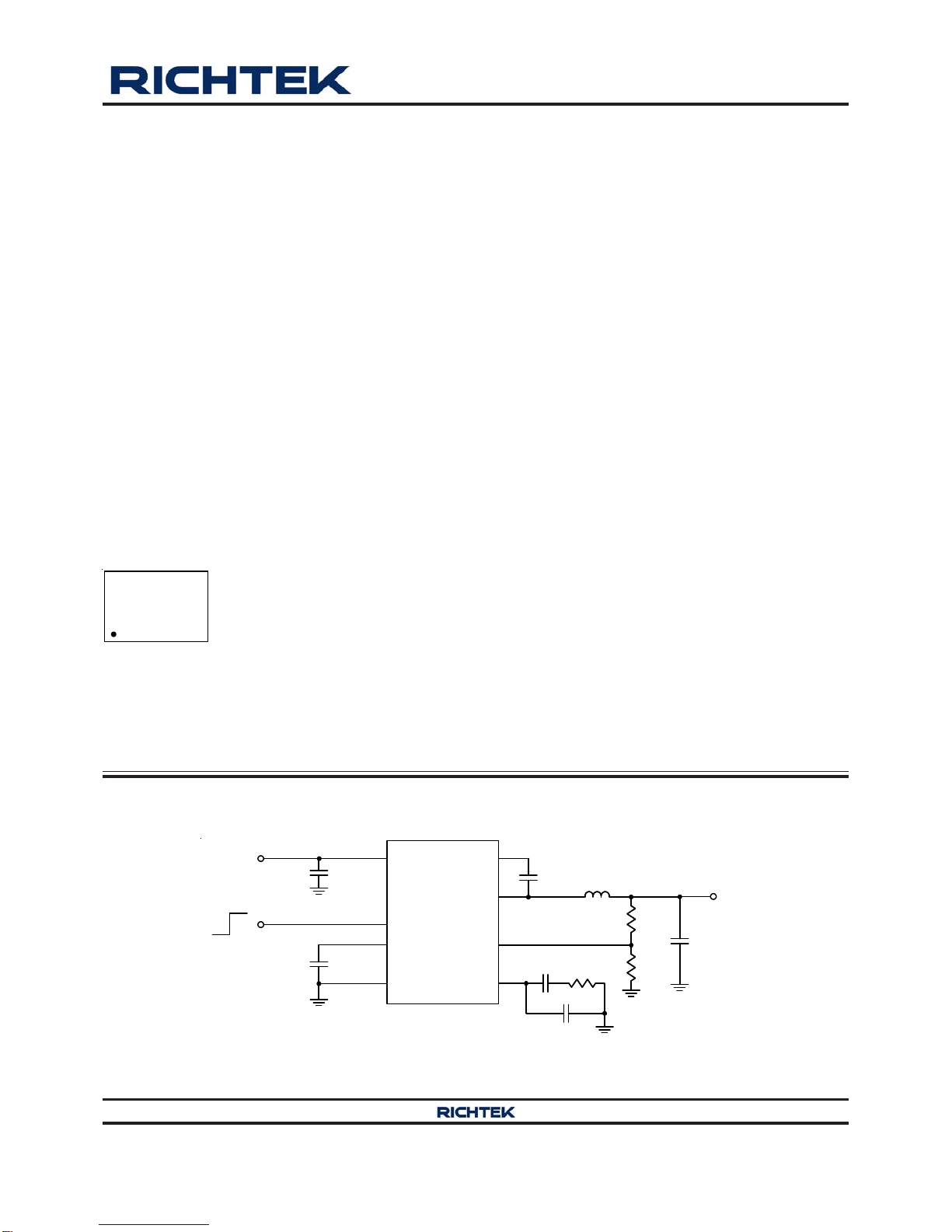
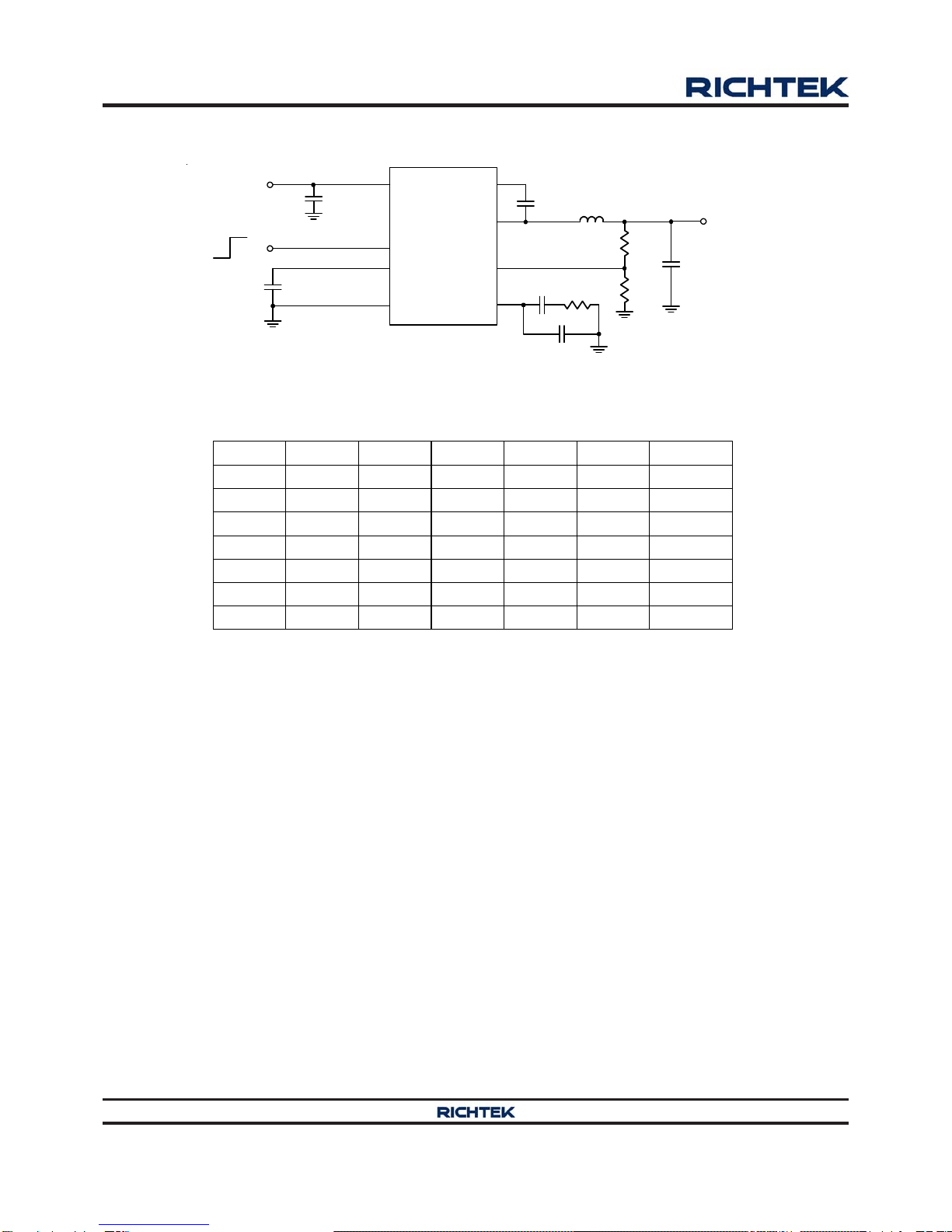
Application Information
Output Voltage Setting
TheresistivedividerallowstheFBpin to sense the output
voltage as shown in Figure 1.
Figure 1. Output Voltage Setting
The output voltage is set by an external resistive voltage
divideraccordingto the followingequation:
OUT REF R1
V =V 1
R2
Where VREF is the reference voltage (0.8V typ.).
External Bootstrap Diode
Connecta0.1μFlowESRceramic capacitor between the
BOOT pin and SW pin. This capacitor provides the gate
drivervoltageforthehighsideMOSFET.
It is recommended to add an external bootstrap diode
between an external 5V and BOOT pin for efficiency
improvementwheninputvoltageis lowerthan5.5Vorduty
ratio is higher than 65% .The bootstrap diode can be a
low cost one such as IN4148 or BAT54. The external 5V
can be a 5V fixed input from system or a 5V output of the
RT7247A. Note that the external boot voltage must be
lowerthan 5.5V
Figure 2. External BootstrapDiode
Chip Enable Operation
The EN pin is the chip enable input. Pulling the EN pin
low (<0.4V) will shut down the device. During shutdown
mode,theRT7247A quiescentcurrentdropstolower than
3μA.Driving the ENpin high (>2V, <18V) will turn on the
device again. For external timing control, the ENpin can
also be externally pulled high by adding a REN resistor
and CEN capacitor from theVINpin (see Figure 3).
Soft-Start
The RT7247A provides soft-start function. The soft-start
function is used to prevent large inrush current while
converter is being powered-up. The soft-start timing can
beprogrammedbytheexternalcapacitorbetweenSSand
GND. An internal current source ISS (6μA) charges an
external capacitor to build a soft-start ramp voltage. The
VFB voltagewilltracktheinternalramp voltage duringsoft-
start interval. The typical soft start time is calculated as
follows :
SS
SS SS
SS
0.8 C
Soft-Start time t = , if C capacitor
I0.8 0.1
is 0.1 F, then soft-start time = 13.5ms
6
≒
An external MOSFET can be added to implement digital
controlontheENpin when nosystemvoltageabove2.5V
is available, as shown in Figure 4. In this case, a 100kΩ
pull-up resistor, REN, is connected between VIN and the
EN pin. MOSFET Q1 will be under logic control to pull
down the EN pin.
Figure3.EnableTimingControl
Figure 4.Digital Enable Control Circuit
RT7247A
GND
FB
R1
R2
VOUT
SW
BOOT
5V
RT7247A 100nF
RT7247A
EN
GND
VIN REN
CEN
EN
RT7247A
EN
GND
100k
VIN
REN
Q1
EN

RT7247A
11
DS7247A-03 October 2016 www.richtek.com
©
Copyright 2016 Richtek Technology Corporation. All rights reserved. is a registered trademark of Richtek Technology Corporation.
Under Voltage Protection
Hiccup Mode
FortheRT7247AH,itprovidesHiccupModeUnderVoltage
Protection(UVP).WhentheVFB voltage dropsbelow0.4V,
theUVPfunctionwill be triggered to shut down switching
operation. If the UVP condition remains for a period, the
RT7247AH will retry automatically. When the UVP
conditionisremoved,the converter willresumeoperation.
The UVP is disabled during soft-start period.
Figure 5. Hiccup Mode Under Voltage Protection
Latch-Off Mode
For the RT7247AL, it provides Latch-Off Mode Under
Voltage Protection (UVP). When the FB voltage drops
below half of the feedback reference voltage, VFB, UVP
willbetriggeredandtheRT7247ALwillshutdown inLatch-
Off Mode. In shutdown condition, the RT7247AL can be
reset by EN pin or power input VIN.
Figure6.Latch-OffModeUnderVoltageProtection
OUT OUT
LIN
VV
I = 1
fL V
Having a lower ripple current reduces not only the ESR
lossesintheoutputcapacitors butalsotheoutputvoltage
ripple.Highfrequencywithsmall ripplecurrent canachieve
the highest efficiency operation. However, it requires a
large inductor to achieve this goal.
Fortheripplecurrentselection,the valueofΔIL=0.24(IMAX)
will be a reasonable starting point. The largest ripple
current occurs at the highest VIN. To guarantee that the
Over Temperature Protection
The RT7247Afeatures an Over Temperature Protection
(OTP) circuitry to prevent from overheating due to
excessive power dissipation. The OTP will shut down
switching operation when junction temperature exceeds
150°C. Once the junction temperature cools down by
approximately20°C,theconverterwillresumeoperation.
To maintaincontinuousoperation,themaximum junction
temperatureshouldbelowerthan125°C.
Inductor Selection
Theinductorvalueandoperating frequencydeterminethe
ripple current according to a specific input and output
voltage. The ripple current ΔILincreases with higher VIN
anddecreases with higher inductance.
Clamp Mode
For the RT7247AN, it provides inductor current clamp
mode.
Figure7.Clamp Mode
Time (1ms/Div)
Clamp Mode
VOUT
(2V/Div)
ILX
(1A/Div) IOUT = Short
Time (25ms/Div)
Hiccup Mode
VOUT
(2V/Div)
ILX
(1A/Div) IOUT = Short
Time (25μs/Div)
Latch-Off Mode
VOUT
(2V/Div)
ILX
(2A/Div)
IOUT = Short

RT7247A
12 DS7247A-03 October 2016www.richtek.com
©
Copyright 2016 Richtek Technology Corporation. All rights reserved. is a registered trademark of Richtek Technology Corporation.
OUT IN
RMS OUT(MAX) IN OUT
VV
I =I 1
VV
CIN and COUT Selection
The input capacitance, CIN, is needed to filter the
trapezoidalcurrentatthesourceofthehighsideMOSFET.
To preventlargeripplecurrent,a low ESR inputcapacitor
sizedforthemaximumRMScurrentshouldbeused.The
approximate RMS current equation is given :
This formula has a maximum at VIN = 2VOUT, where
IRMS = IOUT / 2. This simple worst case condition is
commonly used for design because even significant
deviationsdonotoffermuch relief.
Choose a capacitor rated at a higher temperature than
required. Several capacitors may also be paralleled to
meet size or height requirements in the design.
For the input capacitor, two 10μF low ESR ceramic
capacitors are suggested. For the suggested capacitor,
please refer to Table 3 for more details.
Theselection of COUT isdeterminedby the required ESR
to minimize voltage ripple.
Moreover, the amount of bulk capacitance is also a key
forCOUT selectiontoensurethatthecontrolloop is stable.
OUT L OUT
1
VIESR
8fC
Theoutputripplewillbethehighest at the maximum input
voltage since ΔIL increases with input voltage. Multiple
capacitors placed in parallel may be needed to meet the
ESRandRMScurrenthandlingrequirement.Highervalues,
lowercostceramiccapacitorsarenowbecoming available
insmallercasesizes.Theirhighripplecurrent,highvoltage
ratingandlow ESRmakethemidealforswitchingregulator
applications. However, care must be taken when these
capacitors are used at input and output. When a ceramic
capacitor is used at the input and the power is supplied
by a wall adapter through long wires, a load step at the
output can induce ringing at the input, VIN. At best, this
ringing can couple to the output and be mistaken as loop
instability. At worst, a sudden inrush of current through
the long wires can potentially cause a voltage spike at
VIN large enough to damage the part.
Thermal Considerations
For continuous operation, do not exceed the maximum
operation junction temperature 125°C. The maximum
power dissipation depends on the thermal resistance of
IC package, PCB layout, the rate of surroundings airflow
andtemperaturedifferencebetweenjunctiontoambient.
The maximum power dissipation can be calculated by
followingformula:
PD(MAX) = (TJ(MAX) − TA ) / θJA
Where TJ(MAX) is the maximum operation junction
temperature,TAis theambient temperatureandtheθJAis
the junction to ambient thermal resistance.
Forrecommendedoperatingconditionspecifications,the
maximumjunction temperature is 125°C. The junctionto
ambient thermal resistance θJA is layout dependent. For
SOP-8 (Exposed Pad) package, the thermal resistance
θJA is 75°C/W on the standard JEDEC 51-7 four-layers
thermal test board. The maximum power dissipation at
TA= 25°C can be calculated by following formula :
Table 2. Suggested Inductors for Typical
Application Circuit
Component
Supplier Series Dimensions
(mm)
TDK VLF10045 10 x 9.7 x 4.5
TDK SLF12565 12.5 x 12.5x 6.5
TAIYO
YUDEN NR8040 8 x 8 x 4
OUT OUT
L(MAX) IN(MAX)
VV
L = 1
fI V
Theinductor'scurrentrating(causeda40°Ctemperature
rising from 25°C ambient) should be greater than the
maximum load current and its saturation current should
begreaterthanthe short circuit peak current limit.Please
see Table 2 for the inductor selection reference.
ripple current stays below the specified maximum, the
inductorvalueshould bechosenaccordingtothefollowing
equation :
Loopstabilitycanbecheckedbyviewing theloadtransient
response as described in a later section.
The output ripple, ΔVOUT , is determined by :

RT7247A
13
DS7247A-03 October 2016 www.richtek.com
©
Copyright 2016 Richtek Technology Corporation. All rights reserved. is a registered trademark of Richtek Technology Corporation.
PD(MAX) = (125°C −25°C) / (75°C/W) = 1.333W
(min.copper area PCB layout)
PD(MAX) = (125°C −25°C) / (49°C/W) = 2.04W
(70mm2copperareaPCBlayout)
The thermal resistance θJA of SOP-8 (Exposed Pad) is
determined by the package architecture design and the
PCB layout design. However, the package architecture
designhasbeendesigned.Ifpossible,it'susefultoincrease
thermal performance by the PCB layout copper design.
The thermal resistance θJA can be decreased by adding
copper area under the exposed pad of SOP-8 (Exposed
Pad) package.
AsshowninFigure8,theamountofcopperareatowhich
the SOP-8 (Exposed Pad) is mounted affects thermal
performance. When mounted to the standard
SOP-8 (Exposed Pad) pad (Figure 8.a), θJA is 75°C/W.
Adding copper area of pad under the SOP-8 (Exposed
Pad) (Figure8.b)reducestheθJA to64°C/W. Evenfurther,
increasing the copper area of pad to 70mm2(Figure 8.e)
reduces the θJA to 49°C/W.
The maximum power dissipation depends on operating
ambient temperature for fixed TJ(MAX) and thermal
resistance θJA.TheFigure9ofderatingcurvesallowsthe
designer to see the effect of rising ambient temperature
on the maximum power dissipation allowed.
Figure9.DeratingCurveofMaximumPowerDissipation
0.0
0.2
0.4
0.6
0.8
1.0
1.2
1.4
1.6
1.8
2.0
2.2
0 25 50 75 100 125
Ambient Temperature (°C)
Power Dissipation (W)
Copper Area
70mm2
50mm2
30mm2
10mm2
Min.Layout
Four-Layer PCB
(a) Copper Area = (2.3 x 2.3) mm2,θJA = 75°C/W
(b) CopperArea = 10mm2,θJA = 64°C/W
(c) Copper Area = 30mm2,θJA = 54°C/W
(d) CopperArea = 50mm2,θJA = 51°C/W
(e) CopperArea = 70mm2,θJA = 49°C/W
Figure8.ThermalResistance vs. CopperArea Layout
Design

RT7247A
14 DS7247A-03 October 2016www.richtek.com
©
Copyright 2016 Richtek Technology Corporation. All rights reserved. is a registered trademark of Richtek Technology Corporation.
Layout Consideration
FollowthePCBlayoutguidelinesforoptimalperformance
oftheRT7247A.
Keep the traces of the main current paths as short and
wide as possible.
Puttheinputcapacitorascloseaspossibletothedevice
pins(VINandGND).
SW node is with high frequency voltage swing and
shouldbekeptatsmallarea.Keepanalogcomponents
awayfromthe SWnodetopreventstraycapacitivenoise
pick-up.
Connectfeedbacknetworkbehindtheoutputcapacitors.
Keep the loop area small. Place the feedback
components nearthe RT7247A.
An example of PCB layout guide is shown in Figure 10
forreference.
Figure 10. PCB LayoutGuide
Table 3. Suggested Capacitors for CIN and COUT
Location Component Supplier Part No. Capacitance (F) Case Size
CIN MURATA GRM31CR61E106K 10 1206
CIN TDK C3225X5R1E106K 10 1206
CIN TAIYO YUDEN TMK316BJ106ML 10 1206
COUT MURATA GRM31CR60J476M 47 1206
COUT TDK C3225X5R0J476M 47 1210
COUT MURATA GRM32ER71C226M 22 1210
COUT TDK C3225X5R1C22M 22 1210
VIN
VOUT
GND
CIN
GND
CP
CC
RC
SW
VOUT
COUT
L
R1
R2
Input capacitor must
be placed as close
to the IC as possible.
SW node is with high frequency voltage swing and should
be kept at small area. Keep analog components away from
the SW node to prevent stray capacitive noise pick-up
The feedback components
must be connected as close
to the device as possible.
BOOT
VIN
SW
GND
SS
EN
FB
COMP
GND
2
3
45
6
7
8
9
CSS
GND VIN
REN
CBOOT

RT7247A
15
DS7247A-03 October 2016 www.richtek.com
Richtek Technology Corporation
14F, No. 8, Tai Yuen 1st Street, Chupei City
Hsinchu, Taiwan, R.O.C.
Tel: (8863)5526789
Richtek products are sold by description only. Richtek reserves the right to change the circuitry and/or specifications without notice at any time. Customers should
obtain the latest relevant information and data sheets before placing orders and should verify that such information is current and complete. Richtek cannot
assume responsibility for use of any circuitry other than circuitry entirely embodied in a Richtek product. Information furnished by Richtek is believed to be
accurate and reliable. However, no responsibility is assumed by Richtek or its subsidiaries for its use; nor for any infringements of patents or other rights of third
parties which may result from its use. No license is granted by implication or otherwise under any patent or patent rights of Richtek or its subsidiaries.
Outline Dimension
A
B
J
F
H
M
C
D
I
Y
X
EXPOSED THERMAL PAD
(Bottom of Package)
8-Lead SOP (Exposed Pad) Plastic Package
Symbol Dimensions In Millimeters Dimensions In Inches
Min Max Min Max
A 4.801 5.004 0.189 0.197
B 3.810 4.000 0.150 0.157
C 1.346 1.753 0.053 0.069
D 0.330 0.510 0.013 0.020
F 1.194 1.346 0.047 0.053
H 0.170 0.254 0.007 0.010
I 0.000 0.152 0.000 0.006
J 5.791 6.200 0.228 0.244
M 0.406 1.270 0.016 0.050
Option 1 X 2.000 2.300 0.079 0.091
Y 2.000 2.300 0.079 0.091
Option 2 X 2.100 2.500 0.083 0.098
Y 3.000 3.500 0.118 0.138
Table of contents
Other Richtek Media Converter manuals