Richtek RT8509A User manual

RT8509A
®
DS8509A-00 November 2013 www.richtek.com
1
©
Copyright 2013 Richtek Technology Corporation. All rights reserved. is a registered trademark of Richtek Technology Corporation.
4.5A Step-Up DC/DC Converter
General Description
The RT8509A is a high performance switching Boost
converter that provides a regulated supply voltage for active
matrix thin film transistor (TFT) liquid crystal displays
(LCDs).
The RT8509A incorporates current mode, fixed-frequency,
pulse width modulation (PWM) circuitry with a built in
N-MOSFET to achieve high efficiency and fast transient
response.
The RT8509A has a wide input voltage range from 2.8V to
14V. In addition, the output voltage can be adjusted up to
24V via an external resistive voltage divider. The maximum
peak current is limited to 4.5A (min.). Other features
include adjustable soft-start, over-voltage protection, and
over-temperature protection.
The RT8509A is available in the WDFN-12L 5x5 package.
Features
90%Efficiency
Adjustable Output Up to 24V
2.8V to 14V Input Supply Voltage
Input Supply Under-Voltage Lockout
Fixed 1.2MHz Switching Frequency
Adjustable Soft-Start
VOUT Over-Voltage Protection
Over-Temperature Protection
Thin 12-Lead WDFN Package
RoHS Compliant and Halogen Free
Applications
GIP TFT-LCD Panels
Ordering Information
Note :
Richtek products are :
RoHS compliant and compatible with the current require-
ments of IPC/JEDEC J-STD-020.
Suitable for use in SnPb or Pb-free soldering processes.
Package Type
QW : WDFN-12L 5x5 (W-Type)
RT8509A
Lead Plating System
G : Green (Halogen Free and Pb Free)
LX
RT8509A
VIN
EN
VOUT
FB
SS
COMPGND
R1
R2
COUT
VOUT
CSS
R3
C1
C2
R4
CIN
VIN
L1 D1
C3
Enable
Marking Information
RT8509A
GQW
YMDNN
RT8509AGQW : Product Number
YMDNN : Date Code
Simplified Application Circuit

RT8509A
2
DS8509A-00 November 2013www.richtek.com
©
Copyright 2013 Richtek Technology Corporation. All rights reserved. is a registered trademark of Richtek Technology Corporation.
Functional Pin Description
Pin No. Pin Name Pin Function
1 COMP
Compensation Node for Error Amplifier. Connect a series RC from COMP to
ground.
2 FB
Feedback Voltage Input. The FB regulation voltage is 1.25V nominal. Connect an
external resistive voltage divider between the step-up regulator’s output (VOUT)
and GND, with the center tap connected to FB. Place the divider close to the IC
and minimize the trace area to reduce noise coupling.
3 EN Enable Control Input. Drive EN low to turn off the Boost.
4, 5, 6, 9,
13 (Exposed Pad) GND Ground. The Exposed Pad must be soldered to a large PCB and connected to
GND for maximum power dissipation.
7, 8 LX Switch Node. LX is the Drain of the internal MOSFET. Connect the
inductor/rectifier diode junction to LX and minimize the trace area for lower EMI.
10 VOUT
Over-Voltage Protection Input for Boost Converter. Bypass VOUT with a
minimum 1F ceramic capacitor directly to GND.
11 VIN Supply Voltage Input. Bypass VIN with a minimum 1μF ceramic capacitor directly
to GND.
12 SS
Soft-Start Time Setting. Connect a soft-start capacitor (CSS) to this pin. The
soft-start capacitor is charged with a constant current of 5A. The soft-start
capacitor is discharged to ground when EN is low.
Pin Configurations
WDFN-12L 5x5
(TOP VIEW)
COMP
FB
GND
GND
SS
VIN
VOUT
LX
GND
EN
GND LX
GND
13
11
10
9
1
2
3
4
5
12
67
8

RT8509A
3
DS8509A-00 November 2013 www.richtek.com
©
Copyright 2013 Richtek Technology Corporation. All rights reserved. is a registered trademark of Richtek Technology Corporation.
Function Block Diagram
Operation
The RT8509A is a high-performance step-up DC/DC
converter that provides a regulated and high precision
supply voltage. It incorporates current mode, fixed-
frequency, pulse-width modulation (PWM) circuitry with
a built-in N-Channel power MOSFET to achieve high
efficiency and fast transient response. The device features
an adjustable soft start time using an external soft-start
capacitor to reduce in-rush current.
Soft
Start
Control
and
Driver
Logic
Current
Sense
Protection
+
-
+
-
Slope
Compensation
Oscillator
OVP
LX
OTP
Error Amplifier
VDD
1.25V
FB
COMP
EN
VIN
VOUT
Summing
Comparator
LX
SS
GND
Clock

RT8509A
4
DS8509A-00 November 2013www.richtek.com
©
Copyright 2013 Richtek Technology Corporation. All rights reserved. is a registered trademark of Richtek Technology Corporation.
Electrical Characteristics
Recommended Operating Conditions (Note 4)
Ambient Temperature Range -------------------------------------------------------------------------------------------- −40°C to 85°C
Junction Temperature Range -------------------------------------------------------------------------------------------- −40°C to 125°C
Absolute Maximum Ratings (Note 1)
LX toGND ------------------------------------------------------------------------------------------------------------------- −0.3V to 28V
VIN, EN to GND ------------------------------------------------------------------------------------------------------------ −0.3V to 16.5V
Other Pins------------------------------------------------------------------------------------------------------------------- −0.3V to 6.5V
Power Dissipation, PD@ TA= 25°C
WDFN-12L 5x5 ------------------------------------------------------------------------------------------------------------- 3.38W
Package Thermal Resistance (Note 2)
WDFN-12L 5x5, θJA ------------------------------------------------------------------------------------------------------- 29.5°C/W
WDFN-12L 5x5, θJC ------------------------------------------------------------------------------------------------------- 7.5°C/W
Junction Temperature ----------------------------------------------------------------------------------------------------- 150°C
Storage Temperature Range -------------------------------------------------------------------------------------------- −65°C to 150°C
Lead Temperature (Soldering, 10sec.) -------------------------------------------------------------------------------- 260°C
ESD Susceptibility (Note 3)
HBM (Human Body Model) ---------------------------------------------------------------------------------------------- 2kV
MM (Machine Model) ----------------------------------------------------------------------------------------------------- 200V
(VIN = 3.3V, VOUT = 10V, TA=25°C unless otherwise specified)
Parameter Symbol Test Conditions Min Typ Max Unit
Supply Current
Input Voltage Range VIN 2.8 -- 14 V
Output Voltage Range VOUT -- -- 24 V
Under Voltage Lockout
Threshold VUVLO V
IN Rising -- 2.5 3 V
UVLO Hysteresis VUVLO -- 200 -- mV
VFB = 1.3V, LX Not Switching -- 1 --
VIN Quiescent Current IQVFB = 1V, LX Switching -- 5 -- mA
Thermal Shutdown Threshold TSD Temperature Rising -- 155 -- C
Thermal Shutdown
Hysteresis TSD -- 10 --
C
VOUT Over Voltage
Threshold VOUT Rising -- 26 -- V
Oscillator
Oscillator Frequency fOSC 1000 1200 1500 kHz
Maximum Duty Cycle DMAX -- 90 -- %
Error Amplifier
FB Regulation Voltage VREF 1.2312 1.25 1.2688 V
FB Input Bias Current IFB -- -- 100 nA
FB Line Regulation -- 0.05 0.2 %/V

RT8509A
5
DS8509A-00 November 2013 www.richtek.com
©
Copyright 2013 Richtek Technology Corporation. All rights reserved. is a registered trademark of Richtek Technology Corporation.
Parameter Symbol Test Conditions Min Typ Max Unit
Transconductance gm I = ±2.5μA at VCOMP = 1V -- 100 --
A/V
Voltage Gain AVFB to COMP -- 700 -- V/V
N-MOSFET
Current Limit ILIM 4.5 5 -- A
On-Resistance RDS(ON) -- 100 250
m
Leakage Current ILEAK V
LX = 24V -- 30 45
A
Current Sense
Transresistance RCS -- 0.25 -- V/A
Soft-Start
Charge Current -- 5 -- A
Control Inputs
Logic-High VIH 1.5 -- --
EN Input
Voltage Logic-Low VIL -- -- 0.5
V
Note 1. Stresses beyond those listed “Absolute Maximum Ratings”may cause permanent damage to the device. These are
stress ratings only, and functional operation of the device at these or any other conditions beyond those indicated in
the operational sections of the specifications is not implied. Exposure to absolute maximum rating conditions may
affect device reliability.
Note 2. θJA is measured at TA= 25°C on a high effective thermal conductivity four-layer test board per JEDEC 51-7. θJC is
measured at the exposed pad of the package.
Note 3. Devices are ESD sensitive. Handling precaution is recommended.
Note 4. The device is not guaranteed to function outside its operating conditions.

RT8509A
6
DS8509A-00 November 2013www.richtek.com
©
Copyright 2013 Richtek Technology Corporation. All rights reserved. is a registered trademark of Richtek Technology Corporation.
Typical Application Circuit
LX
RT8509A
VIN
EN
VOUT
FB
SS
COMP
GND
2
12
1
R1
R2
COUT
VOUT
18V
CSS
R3
C1
7, 8
11
3
10
C2
R4
CIN
VIN
12V
4, 5, 6, 9,
13 (Exposed Pad)
L1
D1
10µF x 3
10
1µF
4.7µH
134k
10k
10µF x 4
33nF
56k
1nF
C3
1µF
Enable

RT8509A
7
DS8509A-00 November 2013 www.richtek.com
©
Copyright 2013 Richtek Technology Corporation. All rights reserved. is a registered trademark of Richtek Technology Corporation.
Boost Reference Voltage vs. Input Voltage
1
1.1
1.2
1.3
1.4
1.5
2 4 6 8 101214
Input Voltage (V)
Boost Reference Voltage (V)
Typical Operating Characteristics
Boost Efficiency vs. Load Current
50
60
70
80
90
100
0 0.3 0.6 0.9 1.2 1.5
Load Current (A)
Boost Efficiency (%)
VOUT = 18V, fOSC = 1.2MHz
VIN = 14V
VIN = 12V
VIN = 10V
Boost Efficiency vs. Load Current
50
60
70
80
90
100
0 0.1 0.2 0.3 0.4 0.5
Load Current (A)
Boost Efficiency (%)
VOUT = 13.5V, fOSC = 1.2MHz
VIN = 3.3V
VIN = 5V
Boost Reference Voltage vs. Temperature
1
1.1
1.2
1.3
1.4
1.5
-50 -25 0 25 50 75 100 125
Temperature (°C)
Boost Reference Voltage (V)
VIN = 3.3V
Boost Frequency vs. Temperature
900
1000
1100
1200
1300
1400
-50 -25 0 25 50 75 100 125
Temperature (°C)
Boost Frequency (kHz
)
VIN = 3.3V
Boost Current Limit vs. Input Voltage
3
4
5
6
7
8
2 4 6 8 10 12 14
Input Voltage (V)
Boost Current Limit (A)

RT8509A
8
DS8509A-00 November 2013www.richtek.com
©
Copyright 2013 Richtek Technology Corporation. All rights reserved. is a registered trademark of Richtek Technology Corporation.
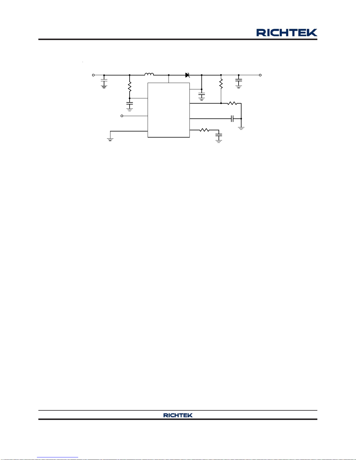
Application Information
The RT8509A is a high performance step-up DC/DC
converter that provides a regulated supply voltage for panel
source driver ICs. The RT8509A incorporates current mode,
fixed frequency, Pulse Width Modulation (PWM) circuitry
with a built-in N-MOSFET to achieve high efficiency and
fast transient response. The internal driver power is
supplied from the VOUT pin and that will increase efficiency
when low input voltage condition. The following content
contains detailed description and information for
component selection.
BoostRegulator
The RT8509A is a current mode Boost converter integrated
with a 24V/5A power switch, covering a wide VIN range
from 2.8V to 14V. It performs fast transient responses to
generate source driver supplies for TFT-LCD display. The
high operation frequency allows the use of smaller
components to minimize the thickness of the LCD panel.
The output voltage can be adjusted by setting the resistive
voltage-divider sensing at the FB pin. The error amplifier
varies the COMP voltage by sensing the FB pin to regulate
the output voltage. For better stability, the slope
compensation signal summed with the current sense
signal will be compared with the COMP voltage to
determine the current trip point and duty cycle. The Boost
minimum gain ratio depends on minimum on-time. It's
suggested that VOUT higher than 1.2 x VIN for better
performance.
Soft-Start
The RT8509A provides soft-start function to minimize the
inrush current. When powered on, an internal constant
current charges an external capacitor. The rising voltage
rate on the COMP pin is limited from VSS = 0V to 1.24V
and the inductor peak current will also be limited at the
same time. When powered off, the external capacitor will
be discharged until the next soft-start time.
The soft-start function is implemented by the external
capacitor with a 5μA constant current charging to the soft-
start capacitor. Therefore, the capacitor should be large
enough for output voltage regulation. A typical value for
soft-start capacitor is 33nF. The available soft-start capacitor
range is from 10nF to 100nF.
OUT REF REF
R1
V = V x 1 , where V = 1.25V (typ.)
R2
The recommended value for R2 should be at least 10kΩ
without some sacrificing. Place the resistive voltage divider
as close as possible to the chip to reduce noise sensitivity.
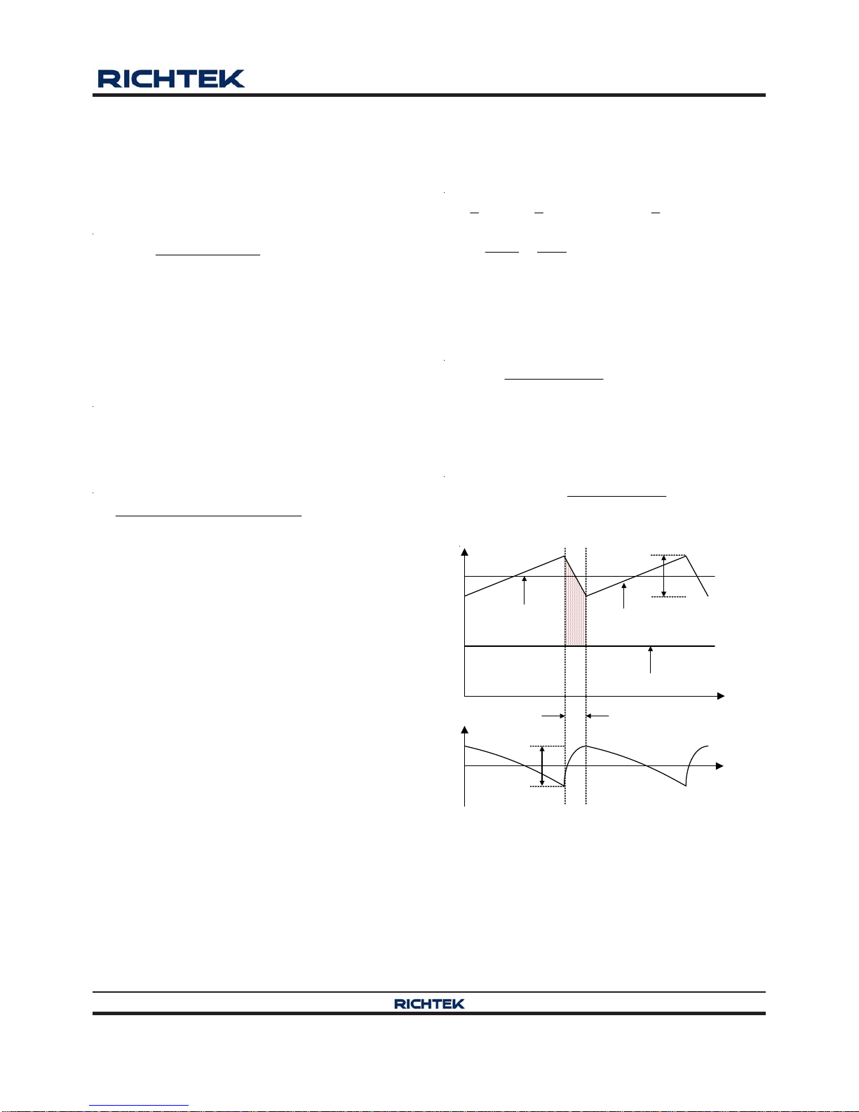
Loop Compensation
The voltage feedback loop can be compensated with an
external compensation network consisting of R3. Choose
R3 to set high frequency integrator gain for fast transient
response and C1 to set the integrator zero to maintain
loop stability. For typical application, VIN = 5V,
VOUT = 13.6V, COUT = 4.7μF x 3, L1 = 4.7μH, while the
recommended value for compensation is as follows :
R3 = 56kΩ, C1 = 1nF.
Over-Current Protection
The RT8509A Boost converter has over-current protection
to limit the peak inductor current. It prevents the inductor
and diode from damage due to large current. During the
On-time, once the inductor current exceeds the current
limit, the internal LX switch turns off immediately and
shortens the duty cycle. Therefore, the output-voltage
drops if the over current condition occurs. The current
limit is also affected by the input voltage, duty cycle, and
inductor value.
Over-Temperature Protection
The RT8509A Boost converter has thermal protection
function to prevent the chip from overheating. When the
junction temperature exceeds 155°C, the function shuts
down the device. Once the device cools down by
approximately 10°C, it will automatically restart to normal
operation. To guarantee continuous operation, do not
operate over the maximum junction temperature rating of
125°C.
If CSS < 220pF, the internal soft-start function will be turned
on and period time is approximately 1ms.
Output Voltage Setting
The regulated output voltage is shown as the following
equation :

RT8509A
9
DS8509A-00 November 2013 www.richtek.com
©
Copyright 2013 Richtek Technology Corporation. All rights reserved. is a registered trademark of Richtek Technology Corporation.
where ηis the efficiency of the converter, IIN(MAX) is the
maximum input current, and IRIPPLE is the inductor ripple
current. The input peak current can then be obtained by
adding the maximum input current with half of the inductor
ripple current as shown in the following equation :
PEAK IN(MAX)
I1.2xI
Note that the saturated current of the inductor must be
greater than IPEAK. The inductance can eventually be
determined according to the following equation :
2
IN OUT IN
2
OUT OUT(MAX) OSC
x (V ) x(V V )
L
0.4 x (V ) xI x f
where fosc is the switching frequency. For better system
performance, a shielded inductor is preferred to avoid EMI
problems.
Diode Selection
Schottky diodes are chosen for their low forward voltage
drop and fast switching speed. When selecting a Schottky
diode, important parameters such as power dissipation,
reverse voltage rating, and pulsating peak current should
all be taken into consideration. A suitable Schottky diode's
reverse voltage rating must be greater than the maximum
output voltage and its average current rating must exceed
the average output current. Last of all, the chosen diode
should have a sufficiently low leakage current level, since
it will increase with temperature.
Output Capacitor Selection
The output ripple voltage is an important index for
estimating chip performance. This portion consists of two
parts. One is the product of the inductor current with the
ESR of the output capacitor, while the other part is formed
by the charging and discharging process of the output
OUT OUT(MAX)
IN(MAX)
IN
RIPPLE IN(MAX)
V xI
I = x V
I = 0.4 x I
Inductor Selection
The inductance depends on the maximum input current.
As a general rule, the inductor ripple current range is 20%
to 40% of the maximum input current. If 40% is selected
as an example, the inductor ripple current can be
calculated according to the following equations : IN L OUT IN L OUT
IN OUT OUT1
OUT OSC
11 1
Q xI II I II
22 2
V1
x x C x V
Vf
where fOSC is the switching frequency, and ΔILis the
inductor ripple current. Bring COUT to the left side to
estimate the value of ΔVOUT1 according to the following
equation :
OUT
OUT1
OUT OSC
D x I
Vx C x f
where D is the duty cycle and ηis the Boost converter
efficiency. Finally, taking ESR into account, the overall
output ripple voltage can be determined by the following
equation :
OUT
OUT IN
OUT OSC
D x I
V I x ESR x C x f
The output capacitor, COUT, should be selected accordingly.
Time
Time
Inductor Current
Output Current
Output Ripple
Voltage (ac)
(1-D)TS
ΔVOUT1
ΔIL
Input Current
Figure 1. The Output Ripple Voltage without the
Contribution of ESR
Input Capacitor Selection
Low ESR ceramic capacitors are recommended for input
capacitor applications. Low ESR will effectively reduce
the input voltage ripple caused by switching operation. A
10μF capacitor is sufficient for most applications.
capacitor. As shown in Figure 1, ΔVOUT1 can be evaluated
based on the ideal energy equalization. According to the
definition of Q, the Q value can be calculated as the
following equation :

RT8509A
10
DS8509A-00 November 2013www.richtek.com
©
Copyright 2013 Richtek Technology Corporation. All rights reserved. is a registered trademark of Richtek Technology Corporation.
Nevertheless, this value can be decreased for lower output
current requirement. Another consideration is the voltage
rating of the input capacitor which must be greater than
the maximum input voltage.
Thermal Considerations
For continuous operation, do not exceed absolute
maximum junction temperature. The maximum power
dissipation depends on the thermal resistance of the IC
package, PCB layout, rate of surrounding airflow, and
difference between junction and ambient temperature. The
maximum power dissipation can be calculated by the
following formula :
PD(MAX) = (TJ(MAX) −TA) / θJA
where TJ(MAX) is the maximum junction temperature, TAis
the ambient temperature, and θJA is the junction to ambient
thermal resistance.
For recommended operating condition specifications, the
maximum junction temperature is 125°C. The junction to
ambient thermal resistance, θJA, is layout dependent. For
WDFN-12L 5x5 packages, the thermal resistance, θJA, is
29.5°C/W on a standard JEDEC 51-7 four-layer thermal
test board. The maximum power dissipation at TA= 25°C
can be calculated by the following formula :
PD(MAX) = (125°C −25°C) / (29.5°C/W) = 3.38W for
WDFN-12L 5x5 package
The maximum power dissipation depends on the operating
ambient temperature for fixed TJ(MAX) and thermal
resistance, θJA. The derating curve in Figure 2 allows the
designer to see the effect of rising ambient temperature
on the maximum power dissipation.
Figure 2. Derating Curve of Maximum Power Dissipation
LayoutConsiderations
For high frequency switching power supplies, the PCB
layout is important to get good regulation, high efficiency
and stability. The following descriptions are the guidelines
for better PCB layout.
For good regulation, place the power components as
close as possible. The traces should be wide and short
enough especially for the high current output loop.
The feedback voltage divider resistors must be near the
feedback pin. The divider center trace must be shorter
and the trace must be kept away from any switching
nodes.
The compensation circuit should be kept away from the
power loops and be shielded with a ground trace to
prevent any noise coupling.
Minimize the size of the LX node and keep it wide and
shorter. Keep the LX node away from the FB.
The exposed pad of the chip should be connected to a
strong ground plane for maximum thermal consideration.
0.0
0.5
1.0
1.5
2.0
2.5
3.0
3.5
4.0
0 25 50 75 100 125
Ambient Temperature (°C)
Maximum Power Dissipation (W)1
Four-Layer PCB

RT8509A
11
DS8509A-00 November 2013 www.richtek.com
©
Copyright 2013 Richtek Technology Corporation. All rights reserved. is a registered trademark of Richtek Technology Corporation.
Figure 3. PCB Layout Guide
GND
VOUT
Place the power components
as close as possible. The
traces should be wide and
short especially for the high-
current loop.
COUT
L1
R3
C1
Locate the C2 as close to
the VIN pin as possible.
D1
VIN
CIN
R1
R2
VOUT
VIN
GND R4
C2
VIN
GND
The feedback voltage-divider
resistors must near the feedback
pin. The divider center trace
must be shorter and avoid the
trace near any switching nodes.
COMP
VOUT
LX
LX
FB
EN
GND
GND
1
2
3
4
5
12
11
10
8
7
13
GND
VIN
SS
GND 6
9GND
More GND via and layout area for
better thermal performance.
The switching trace should be wide and
short especially for the high-current loop.
The compensation circuit should be kept away from the power loops and
should be shielded with a ground trace to prevent any noise coupling.
+

RT8509A
12
DS8509A-00 November 2013www.richtek.com
Richtek Technology Corporation
14F, No. 8, Tai Yuen 1st Street, Chupei City
Hsinchu, Taiwan, R.O.C.
Tel: (8863)5526789
Richtek products are sold by description only. Richtek reserves the right to change the circuitry and/or specifications without notice at any time. Customers should
obtain the latest relevant information and data sheets before placing orders and should verify that such information is current and complete. Richtek cannot
assume responsibility for use of any circuitry other than circuitry entirely embodied in a Richtek product. Information furnished by Richtek is believed to be
accurate and reliable. However, no responsibility is assumed by Richtek or its subsidiaries for its use; nor for any infringements of patents or other rights of third
parties which may result from its use. No license is granted by implication or otherwise under any patent or patent rights of Richtek or its subsidiaries.
Outline Dimension
W-Type 12L DFN 5x5 Package
11
2
2
Note : The configuration of the Pin #1 identifier is optional,
but must be located within the zone indicated.
DETAILA
Pin #1 ID and Tie Bar Mark Options
Min. Max. Min. Max.
A 0.700 0.800 0.028 0.031
A1 0.000 0.050 0.000 0.002
A3 0.175 0.250 0.007 0.010
b 0.200 0.300 0.008 0.012
D 4.900 5.100 0.193 0.201
D2 4.250 4.350 0.167 0.171
E 4.900 5.100 0.193 0.201
E2 3.650 3.750 0.144 0.148
e
L 0.350 0.450 0.014 0.018
Symbol DimensionsIn Millimeters DimensionsIn Inches
0.800 0.031
Table of contents
Other Richtek Media Converter manuals