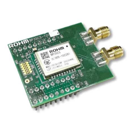
Rohm LAPIS MK71351 User manual

PJDK71351-03
Issue Date:Feb,8,2019
MK71351
BluetoothLow Enegy wireless module
•Bluetooth®is a registered trademark of Bluetooth SIG, Inc.
•All other company and product names are the trademarks or registered trademarks of the respective companies. 1/24
■Overview
MK71351 is a wireless module which is integrating Bluetooth®Specification v4.2 compliant LSI(TC3567CFSG),26MHz/
32.768kHz crystal oscillator, 2.4GHz PCB pattern antenna and passive components.
MK71351 is suitable for applications such as Healthcare, fitness device, Remote Controller or PC peripherals.
■Features
Wireless module wich is integrated 2.4GHz PCB pattern antenna and passive components
Bluetooth® Specification v4.2 low energy compliant
Radio certification
MIC JAPAN(certification no: 006-000680)
FCC(FCC ID: 2ACIJ71351)
ISED(IC: 20971-71351)
CE (RED) EN300 328 V2.1.1
Bluetooth®Qualification(End Product, QDID:xxxxx)
Integrated Bluetooth®Specification v4.2 low enegy compliant LSI (TC3567CFSG)
Integrated 26MHz /32.768kHz crystal oscillator
Integrated NOR Flash Memory(128 KB、105times of erase and program)
Integrated bypass capacitor and external component of switching regulator
RSSI accuracy: ±1 dB(Typ, -85~-10dBm @input,25℃)
●General Purpose Input/Output(13ports)
●General Purpose Serial Interfaces
SPI Inteeface (1 ch assigned to a General Purpose IO)
I2C Interface (1 ch assigned to a General Purpose IO)
●Host Interface
UART Interface(9600bps~921.6kbps、1ch - shared with GPIOs)
SPI Interface
●PWM Interface (3ch、assigned to General Purpose IOs)
●AD Converter
10bit resolution
External analog inputs assigned to GPIOs(3ch)
Internal VDD monitoring (1 ch - connected inside)
Single power supply 2.0V to 3.6V (Typ.3.0V)
Operating Temperature -40 deg.C to 85 deg.C
Current Consumptions
Deep Sleep State 0.05 uA (Typ.)
Sleep State 2.5 uA (Typ.)
Back up State 2.4 uA (Typ.)
Idle State 0.8 mA (Typ.)
Active RX 3.0 mA (Typ.)
Active TX 2.9 mA(Typ.)
Flash Writing 15.6mA (Typ.)
Product name :MK71351-NNNYEZ05B
PKG :M-FLGA33-9.7X11.95-0.75-9Y
Dimension : 9.7mm (W) x 11.95mm (L) x 2.1mm (H)
Pb Free, RoHS compliant
PJDK71351-03
MK71351
2/24
■Block Diagram
ANTENNA
DCDC
LC Filter
X’tal
26MHz
X’tal
32.768kHz
OUT_ANT
RFIO
VBAT
GND
MK71351
VDDIO
Bluetooth®v4.2 LSI
TC3567C
SWDCLK
SWDIO
GPIO
13
RESETX
TMODE
[UART/SPI/I2C/PWM/ADC]
VPGM
VDDCORE

PJDK71351-03
MK71351
3/24
■Pin Layout
TOP VIEW
GND
OUT_ANT
NC
VPGM
TMODE
VDDCORE
GND
RESETX
SWDIO
GND
NC
GPIO1
/mode1
GPIO8
GPIO7
GPIO6
GPIO5
GPIO11
GPIO12
GPIO15
GND
VBAT
VDDIO
GPIO13
GPIO10
GPIO4
GPIO3
SWDCLK
GPIO0
1
2
3
4
5
6
7
8
9
10
11
12
13
14
15
16
17
18
19
20
28
27
26
25
24
23
22
21
29
30
31
32
33
RFIO

PJDK71351-03
MK71351
4/24
■List of Pins
Symbols
IRF
:
RF I/O pin.
ISHPUD
:
Schmitt Trigger input pin with Pull-up, and Pull-down.
Ish
:
Schmitt Trigger input pin
IOSHPUD
:
Schmitt Trigger Digital I/O pin with Pull-up, and Pull-down.
IOASHPUD
Schmitt Trigger Digital I/O with Pull-up, and Pull-down. and analog input pin
Pin
Symbol
Attribute/value
at reset
I/O
Active
level
Description
1
NC
---
---
---
NC Pin
2
OUT_ANT
---
IRF
---
PCB antenna input
(to be connected to RFIO by user's PCB)
3
RFIO
---
IRF
---
RF Input/Output from Module
(to be connected to OUT_ANT by user's PCB)
4
GND
---
---
---
GND
5
VPGM
---
---
---
Test pin
6
TMODE
Input
Ish
---
TEST MODE input (Low = Normal operation)
7
VDDCORE
1.35 V output
---
---
CORE voltage monitor pin
8
GND
---
---
---
GND
9
RESETX
Input
Ish
Low
Reset input (Low = Reset)
10
SWDIO
Input
IOSHPUD
---
Serial wire debugger data pin and operation mode
switching pin
11
GND
---
---
---
GND
12
VBAT
---
---
---
Power supply 2.0 to 3.6 V
13
VDDIO
---
---
---
Power supply 2.0 to 3.6 V
14
GPIO13
Pull-up
IOSHPUD
---
General-purpose IO pin
15
GPIO10
Hi-Z
IOASHPUD
---
ADC input, general-purpose IO pin
16
GPIO4
Hi-Z
IOASHPUD
---
ADC input, general-purpose IO pin
17
GPIO3
Hi-Z
IOASHPUD
---
ADC input, general-purpose IO pin
18
SWDCLK
Input
ISHPUD
---
Serial wire debugger clock pin
19
GPIO0
Hi-Z
IOSHPUD
---
General-purpose IO pin and WakeUp0 input pin
20
GND
---
---
---
GND
21
GPIO15
Hi-Z
IOSHPUD
---
General-purpose IO pin and WakeUp1 input pin
22
GPIO12
Pull-up
IOSHPUD
---
General-purpose IO pin
23
GPIO11
Pull-up
IOSHPUD
---
General-purpose IO pin
24
GPIO5
Pull-up
IOSHPUD
---
General-purpose IO pin
25
GPIO6
Pull-up
IOSHPUD
---
General-purpose IO pin
26
GPIO7
Pull-up
IOSHPUD
---
General-purpose IO pin
27
GPIO8
Pull-up
IOSHPUD
---
General-purpose IO pin
28
GPIO1
Pull-up
IOSHPUD
---
General-purpose IO pin
29
NC
---
---
---
NC pin
30
GND
---
---
---
GND
31
GND
---
---
---
GND
32
GND
---
---
---
GND
33
GND
---
---
---
GND
Note: Pull-up/Pull-down register’s range is 20k~100kΩ.

PJDK71351-03
MK71351
5/24
■Pin Description
Symbols
IRF
:
RF I/O pin.
ISHPUD
:
Schmitt Trigger input pin with Pull-up, and Pull-down.
Ish
:
Schmitt Trigger input pin
IOSHPUD
:
Schmitt Trigger Digital I/O pin with Pull-up, and Pull-down..
IOASHPUD
Schmitt Trigger Digital I/O with Pull-up, and Pull-down. and analog input pin.
●RF, Analog Related Pins
Pin
Symbol
Attribute/value
at reset
I/O
Active
level
Description
2
OUT_ANT
---
IRF
---
PCB antenna input
(to be connected to RFIO by user's PCB)
3
RFIO
---
IRF
---
RF Input/Output from Module
(to be connected to OUT_ANT by user's PCB)
●General-Purpose IO Pins
Pin
Symbol
Attribute/value
at reset
I/O
Active
level
Description
19
GPIO0
Hi-Z
IOSHPUD
---
General-purpose I/O pin
During reset, internal Pull-up/Pull-down resistor
turns OFF and is put into the Disable state.
After the pin configuration by software
processing, this pin can function as a function pin
or a GPIO pin of I/O.
See Table 2-2.
21
GPIO15
Hi-Z
IOSHPUD
---
28
GPIO1
Pull-up
IOSHPUD
---
General-purpose I/O pin
During reset, internal Pull-up resistor turns ON
and is put into the Disable state.
After the pin configuration by software
processing, this pin can function as a function pin
or a GPIO pin of I/O.
GPIO1 is used as a condition for switching the
operation mode.
See List of GPIO Pin Functions section.
24
GPIO5
Pull-up
IOSHPUD
---
25
GPIO6
Pull-up
IOSHPUD
---
26
GPIO7
Pull-up
IOSHPUD
---
27
GPIO8
Pull-up
IOSHPUD
---
23
GPIO11
Pull-up
IOSHPUD
---
22
GPIO12
Pull-up
IOSHPUD
---
17
GPIO3
Hi-Z
IOASHPUD
---
ADC input, general-purpose I/O pin
During reset, internal Pull-up/Pull-down resistor
turns OFF and is put into the Disable state.
After the pin configuration by software
processing, this pin can function as a function
pin, a general-purpose ADC channel pin, or a
GPIO pin of I/O, by selecting either of these.
See List of GPIO Pin Functions section.
16
GPIO4
Hi-Z
IOASHPUD
---
15
GPIO10
Hi-Z
IOASHPUD
---
14
GPIO13
Pull-up
IOSHPUD
---
General-purpose I/O pin
During reset, internal Pull-up resistor turns ON
and is put into the input Disable state.
After the pin configuration by software
processing, this pin can function as a function pin
or a GPIO pin of I/O.
See List of GPIO Pin Functions section.

PJDK71351-03
MK71351
6/24
●Other Pins
Pin
Symbol
Attribute/value
at reset
I/O
Active
level
Description
6
TMODE
Input
Ish
---
TEST MODE input (Low = Normal operation)
9
RESETX
Input
Ish
Low
Reset input (Low = Reset)
●CORE Voltage Related Pins
Pin
Symbol
Attribute/value
at reset
I/O
Active
level
Description
7
VDDCORE
1.35 V output
---
---
CORE voltage monitor pin
Normally, use this pin in the OPEN.
●Debugger Related Pins
Pin
Symbol
Attribute/value
at reset
I/O
Active
level
Description
10
SWDIO
Input
Pull-up
IOSHPUD
---
Serial wire debugger data pin and operation mode switching
pin.
During reset, internal Pull-down resistor turns ON and is put
into the input state. After the reset is released, this pin turns
into the I/O of the serial wire debugger data.
If this function is not used, the pin should be OPEN.
18
SWDCLK
Input
Pull-Down
ISHPUD
---
Serial wire debugger clock pin
During reset, internal Pull-down resistor turns ON and is put
into the input state. After the reset is released, this pin turns
into the input of the serial wire debugger clock.
If this function is not used, the pin should be OPEN.
●Power Supply Pin
Pin
Symbol
Attribute/value
at reset
I/O
Active
level
Description
5
VPGM
---
---
---
Power supply pin for test
Connect this pin to GND.
12
VBAT
---
---
---
Power supply 2.0 to 3.6 V
13
VDDIO
---
---
---
Power supply 2.0 to 3.6 V
4
GND
---
---
---
GND
8
GND
---
---
---
GND
11
GND
---
---
---
GND
20
GND
---
---
---
GND
30
GND
---
---
---
GND
31
GND
---
---
---
GND
32
GND
---
---
---
GND
33
GND
---
---
---
GND
●N.C. Pins
Pin
Symbol
Attribute/value
at reset
I/O
Active
level
Description
1
NC
---
---
---
NC pin, always use in the OPEN.
29
NC
---
---
---
NC pin, always use in the OPEN.

PJDK71351-03
MK71351
7/24
●List of GPIO Pin Functions
The functions of GPIO pins are allocated to the UART interface and serial memory interface, among others, depending on the
firmware implemented to ROM and commands from the external host. This list indicates the hardware state during reset, the
software control setting immediately after the reset is released, and the functions which can be set for each GPIO pin.
When the same function name is allocated to several pins, it is not possible to select several pins to allocate the function at the
same time.
Pin name
State
during
reset
State
immediately
after the reset is
released
Function 1
Function 2
Function 3
Function 4
Analog
input
GPIO0
Disable/
Hi-Z
Disable/
Pull-up,
Pull-down: off
WakeUp0
input
-
-
-
-
GPIO1
Disable/
Pull-up
Input/Pull-up
(*1)
PWM0
output
-
-
-
-
GPIO3
Disable/
Hi-Z
Disable/
Pull-up,
Pull-down: off
PWM2
output
SPI-DOUT
output
-
-
ADC1
input
GPIO4
Disable/
Hi-Z
Disable/
Pull-up,
Pull-down: off
PWM3
output
SPI-DIN
input
-
-
ADC2
input
GPIO5
Disable/
Pull-up
Input/Pull-up
(*2)
UART1-TX
output
SPI-DOUT
output
-
-
-
GPIO6
Disable/
Pull-up
Input/Pull-up
(*2)
UART1-RX
input
SPI-DIN
input
-
-
-
GPIO7
Disable/
Pull-up
Input/Pull-up
I2C-SCL
output
-
SPI-SCS
output
UART1-RTSX
output
-
GPIO8
Disable/
Pull-up
Input/Pull-up
I2C-SDA
I/O
-
SPI-SCLK
output
UART1-CTSX
input
-
GPIO10
Disable/
Hi-Z
Disable/
Pull-up,
Pull-down: off
-
-
-
-
ADC4
input
GPIO11
Disable/
Pull-up
Input/Pull-up
I2C-SCL
output
SPI-DOUT
output
-
-
-
GPIO12
Disable/
Pull-up
Input/Pull-up
I2C-SDA
I/O
SPI-DIN
input
-
-
-
GPIO13
Disable/
Pull-up
Input/Pull-up
-
-
-
-
GPIO15
Disable/
Hi-Z
Disable/
Pull-up,
Pull-down: off
WakeUp1
input
-
-
-
-
(*1) In any mode expect for the User-App mode, this will be Pull-down.
(*2) In the HCI mode, the Pull-up/Pull-down resistance will be OFF.
(*) The state of GPIO pin indicates the state when it is used in the User App mode. When the module is
started in the HCI mode, some pins may have a different state. As to the detailed state of each pin and how to
set it, refer to the Software Application Notes.

PJDK71351-03
MK71351
8/24
●Termination of Unused Pins
See below for the handling of unused pins.
Pin termination which can impair the basic operation of the MK71351 is not included.
Pin
Symbol
Description
1,29
NC
Open
7
VDDCORE
Open
10
SWDIO
Open
14
GPIO13
Open
15
GPIO10
Open
16
GPIO4
Open
17
GPIO3
Open
18
SWDCLK
Open
19
GPIO0
Open
21
GPIO15
Open
22
GPIO12
Open
23
GPIO11
Open
24
GPIO5
Open
25
GPIO6
Open
26
GPIO7
Open
27
GPIO8
Open
28
GPIO1
Open (*1)
(*1) Care should be taken because this pin is used as the operation mode switching pin.

PJDK71351-03
MK71351
9/24
■Electrical Characteristics
The values listed in the section indicated as typical. below represent typical median values. They are not guaranteed values, as
no consideration is given to a variety.
●Absolute Maximum Ratings
Item
Symbol
Condition
Rating
Unit
Power supply voltage
VBAT,
VDDIO (*1)
-0.3 to +3.9
V
Input voltage
VIN
–0.3 to VDDIO+0.3 (*2)
V
Output voltage
VOUT
Ta = 40 to +85 °C
–0.3 to VDDIO+0.3 (*2)
V
Input current
IIN
-10 to +10
mA
Input power
RFIO
+6
dBm
Storage temperature
Tstg
–
-40 to +85
°C
(*1) When voltage is applied to the VDDIO power supply, do not connect VBAT to GND.
Otherwise, current flows from VDDIO to VBAT through the circuit inside IC and may cause breaking, damage, or
deterioration.
(*2) VDDIO+0.3 V should not exceed 3.9 V when using.
●Recommended Operating Conditions
Item
Symbol
Min.
Standard
Max.
Unit
Power supply
voltage
VBAT operating voltage
(*)
VBAT
2.00
3.00
3.60
V
VDDIO operating voltage
VDDIO
2.00
3.00
3.60
V
RF channel frequency
FC
2400
–
2483.5
MHz
ADC
Analog reference voltage
VREFH
2.00
3.00
3.60
V
Analog input voltage
VAIN
GND
–
VREFH
V
Operating temperature
Ta
-40
+25
+85
℃

PJDK71351-03
MK71351
10/24
●Current consumption (Ta=25℃)
Item
Symbol
Condition
Min.
Standard
Max.
Unit
Current consumption
of digital section
IDDDIG
(Active1)
Operating state
-
0.8
-
mA
IDDRD
(FlashRead)
Flash read
-
2.4
-
mA
IDDWR
(FlashWrite)
Flash write
-
15.6
-
mA
Current consumption
of power supply
IDDRX
(Active2)
RF receiving state
-
3.0
-
mA
IDDTX
(Active3)
RF transmitting state (0 dBm)
-
2.9
-
mA
Current consumption
at low power
With connection
IDDS1
(Sleep)
26 MHz crystal oscillation has
stopped
32 kHz crystal oscillation
-
2.5
-
uA
Current consumption
at low power
Without connection
IDDS2
(Backup)
26 MHz crystal oscillation has
stopped
32 kHz crystal oscillation
-
2.4
-
uA
Current consumption
at low power
Without connection
IDDS
(Deep Sleep)
26 MHz crystal oscillation has
stopped
32 kHz crystal oscillation has
stopped
-
0.05
-
uA
(*) Condition: VBAT=VDDIO=3.0V, GND=0V
(*) The operating current of I/O section during active operation varies depending on the buffer setting.
●DC Characteristics (Ta=-40~85℃)
Item
Symbol
Condition
Min.
Standard
Max.
Unit
I/F voltage
condition
Other conditions
High-level input
voltage
VIH
3.0 V
LVCMOS
VBAT
X0.8
-
-
V
Low-level input voltage
VIL
3.0 V
LVCMOS
-
-
VBAT
X0.2
V
High-level output
voltage
VOH
3.0 V
IOH=1 mA
VBAT
- 0.6
-
-
V
Low-level output
voltage
VOL
3.0 V
IOL=1 mA
-
-
0.4
V
(*) Condition: VBAT=VDDIO=3.0V, GND=0V
(*)The target pin is a digital input / digital output pin.

PJDK71351-03
MK71351
11/24
●RF Characteristics (Ta=25℃)
Item
Symbol
Condition
Min.
Standard
Max.
Unit
Transmitter
Maximum transmitter
power
POUT
0 dBm setting value
–
0
–
dBm
Center frequency
tolerance
FCERR
Master Clock tolerance <
40 ppm
-40
0
40
ppm
Modulation data rate
DRATE
–
–
1
–
Mbps
Modulation index
FIDX
–
0.45
0.50
0.55
–
Bandwidth Time
BT
GFSK
–
0.5
–
–
Receiver
Receiver sensitivity
PSENS
PER = 30.8 % (*1)
–
-93.5
-
dBm
Maximum receiving
Power
PRXMAX
PER = 30.8 % (*1)
–
–
-10
dBm
(*) Condition: VBAT=VDDIO=3.0V, GND=0V
(*1) PER=30.8 % corresponds to BER=0.1 %.
●Power Supply Sequence
VBAT
VDDIO
Master Clock
(26MHz)
RESET
Internal LDO
DC/DC
Converter
Sleep Clock
(32.768kHz)
BOOT done
Oscillation
When starting up ,Requires 2.0 V or more
Operation start
Boot Started
LDO On
DC/DC On
→Reset release after stabilization of VDDIO is required
After sleep clock detection, internal power supply is
Switched.
(Temporarily switch to sleep mode)
Should not be VBAT<VDDIO
Oscillation

PJDK71351-03
MK71351
12/24
■Operation Mode
MK71351 has the following operation modes.
Operation mode
General description
HCI mode
The standard operation mode of Bluetooth®.
HCI mode conducts communication between
MK71351 and the host MCU through the UART
interface.
User-App mode
This is the Application mode which downloads
the program code to the built-in SRAM.
It is possible to operate this mode alone without
the external host MCU.
MK71351 chooses the operation mode during the Boot process at the start. Refer to the state of pins indicated below when
choosing the operation mode.
Operation mode
Pin status
Note
GPIO1
HCI mode
Low input
User-App mode
OPEN

PJDK71351-03
MK71351
13/24
●HCI Mode
The following figure shows the protocol stack configuration when MK71351 is set to the HCI mode.
It can transmit/receive HCI commands/events compliant with Bluetooth®v4.2 to/from HOST-CPU through the UART
interface.
●User-App Mode
In this mode, the firmware which is stored in the Flash ROM is downloaded and executed after the Boot operation.
In the User-App mode, the operation is possible without host MCU. This operation assumes a Use Case, in which the data
collected from the sensor device is transferred to another device by using Bluetooth® wireless technology. The following figure
shows the protocol stack configuration when MK71351 is set to the User-App mode.
Bluetooth® Host Stack
Bluetooth® Controller
Bluetooth® Profile
Application
(UART)
MK71351
HOST MCU
Bluetooth®Host Stack
Bluetooth®Controller
MK71351
LBLE framework
User Application
Bluetooth®Manager API

PJDK71351-03
MK71351
14/24
■Module Dimension
Remarks for Mounting the Surface Mount Type Package
Surface mount type package is very sensitive affected by heating from reflow process, humidity during storage.
Therefore, before you perform reflow mounting, contact sales office for the product name, package name, pin number, package
code and desired mounting conditions (reflow method, temperature and times) and storage environment.

PJDK71351-03
MK71351
15/24
■Examples of Application Circuit
●Connection Example in HCI mode
In this example, GPIO pins except for HOST I/F(UART) are unused.
- Application data is written from HCI interface or SWD interface.
- Over the Air (OTA) function can be used to rewrite the application data.
MK71351
NC
OUT_ANT
RFIO
VDDCORE
TMODE
GPIO8
GPIO7
GPIO5
GPIO6
RESETX
VPGM
SWDIO
SWDCLK
GPIO0
GPIO15
GPIO1
VBAT
GND
24
25
26
27
9
19
21
GPIO3
GPIO4
GPIO10
GPIO13
GPIO11
GPIO12
17
16
15
23
22
14
1,29
2
3
Power supply
12
7
5
6
28
4,8,11,20
GND
30,31,32,33
0Ω
RESETX
WAKEUP0
WAKEUP1
UART_RXD
UART_RTS
UART_CTS
UART_TXD
10
18
VDDIO
13
VDD
1kΩ
Operation Mode Setting
HCI
mode
User-App
mode
GPIO1
L
OPEN

PJDK71351-03
MK71351
16/24
●Connection Example in User-App mode
In this example, GPIO pins and SWD pins are unused.
- Application data is written from HCI interface or SWD interface.
- Over the Air (OTA) function can be used to rewrite the application data.
- Please refer to the related manual (MK71351 AT Command Application User’s Manual),when using the AT Command
Application.
Operation mode setting
HCI
mode
User-App
mode
GPIO1
L
OPEN
MK71351
NC
OUT_ANT
RFIO
VDDCORE
TMODE
RESETX
VPGM
GPIO0
GPIO15
VBAT
GND
9
19
21
1,29
2
3
Power supply
12
7
5
6
4,8,11,20
GND
30,31,32,33
0Ω
17
16
26
27
15
23
22
14
GPIO8
GPIO7
GPIO3
GPIO4
GPIO10
GPIO13
GPIO11
GPIO12
VDD
SW
VDDIO
13
1kΩ
SWDIO
SWDCLK
GPIO1
28
10
18
SWD I/F
HCI I/F for Programming
User-application
GPIO5
GPIO6
24
25
UART_RXD
UART_TXD

PJDK71351-03
MK71351
17/24
■Appendix
●Reference Land Pattern

PJDK71351-03
MK71351
18/24
●Metal Keep-Out Area (Recommended Layout)
29.7mm min
10mm
TOP VIEW
Main Board
Metal exclusion zone to edge of board
(no metal on any layer except mechanical LGA pads and RF trace line.)
10mm
3.45mm
0Ω
【Note】
・Main Board: Substrate material is FR4 and substrate thickness is 1.0-1.6 mm.
・Do not place a signal pattern or the GND/VDD area on the lower side of the antenna or the above metal
placement prohibited area

PJDK71351-03
MK71351
19/24
●Radio Certification
MIC JAPAN(certification no 006-000680)
MK71351 complies with MIC JAPAN radio certification.(certification no:006-000680)
FCC(FCC ID: 2ACIJ71351)
This device complies with Part 15 of the FCC Rules.
Operation is subject to the following two conditions:
(1)this device may not cause harmful interference, and (2)this device must accept any interference received, including
interference that may cause undesired operation.
The regulatory label on the final system must include the statement: “Contains FCC ID: 2ACIJ71351" or using electronic
labeling method as documented in KDB 784748.
This equipment complies with FCC radiation exposure limits set forth for an uncontrolled environment.
The antenna used for this transmitter must not be collocated or operating in conjunction with any other antenna or transmitter
within a host device, except in accordance with FCC multi-transmitter product procedures.
The final system integrator must ensure there is no instruction provided in the user manual or customer documentation
indicating how to install or remove the transmitter module except such device has implemented two-ways authentication
between module and the host system.
OEM Responsibilities to comply with FCC Regulations
This module has been certified for integration into products only by OEM integrators under the following condition:
- The transmitter module must not be colocated or operating in conjunction with any other antenna or transmitter.
As long as the conditions above are met, further transmitter testing will not be required. However, the OEM integrator is still
responsible for testing their end-product for any additional compliance requirements required with this module installed (for
example, digital device emissions, PC peripheral requirements, etc.).
IMPORTANT NOTE:
In the event that any of these conditions can not be met (for example the reference trace specified in this manual, or use of a
different antenna), then the FCC authorization is no longer considered valid and the FCC ID can not be used on the final
product. In these circumstances, the OEM integrator will be responsible for re-evaluating the end product (including the
transmitter) and obtaining a separate FCC authorization.
Changes or modification not expressly approved by the party responsible for compliance could void the user’s authority to
operate the equipment.
IC(IC: 20971-71351)
This device complies with Industry Canada’s licence-exempt RSSs. Operation is subject to the following two conditions:
(1) This device may not cause interference; and
(2) This device must accept any interference, including interference that may cause undesired operation of the device.
Le présent appareil est conforme aux CNR d’Industrie Canada applicables aux appareils radio exempts de licence.
L’exploitation est autorisée aux deux conditions suivantes :
(1) l’appareil ne doit pas produire de brouillage;
(2) l’utilisateur de l’appareil doit accepter tout brouillage radioélectrique subi, même si le brouillage est susceptible d’en
compromettre le fonctionnement.
The regulatory label on the final system must include the statement: “Contains IC:20971-71351".
Due to the model size the IC identifier is displayed in this manual only and can not be displayed on the modules label due to
the limited size.
CE(RED)
MK71351 complies with the radio test requirements (EN 300 328 V2.1.1) ,which is based on the RE Directive.
EMC and Safety test that is required for the CE marking should be done in the final end-product.

PJDK71351-03
MK71351
20/24
●Bluetooth SIG Qualification(End Product)
MK71351 is listed on the Bluetooth SIG website as qualified End Products.(QDID:XXXXX)
■Note
- When mounting this product on the double-sided board, do not mount it on the initial mounting side.
(Reflow on the other side from the module mounting side is prohibited.)
- Due to its material characteristic, the sealed case may change color. However, this does not affect the product performance
and its quality.
■Related Documents
The following related documents are available and should be referenced as needed.
-MK71351 SDK related documents:
Download "MK71351 SDK" and related documents from the location related to Bluetooth Low Energy at the LAPIS Support
Site below.
https://www.lapis-semi.com/cgi-bin/MyLAPIS/regi/login.cgi (English)
-TC3567CFSG-002 related documents
Download the below documents from the location related to the technical documentation download website of Bluetooth®ICs
at the below site.
https://toshiba.semicon-storage.com/ap-en/product/wireless-communication/bluetooth/documents.html
▪Hardware datasheet
▪Software application manual
▪Software refarence manual
▪Sample software manual
Table of contents
Other Rohm Control Unit manuals
Popular Control Unit manuals by other brands

Helvest
Helvest DCC100-E user manual

ENGO CONTROLS
ENGO CONTROLS ECB02M230 quick guide

Rockwell Automation
Rockwell Automation Allen-Bradley DM2 Application Technique

Siemens
Siemens 3VA9908-0BC Series operating instructions

Pulsar
Pulsar MSRK Series user manual

welldana
welldana DRYDEN AQUA SPACE installation guide