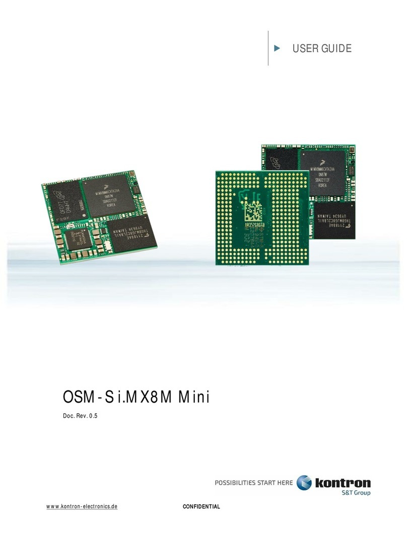
S&T Kontron VX3060 User manual

VX3060 & VX3060-S2 User Guide –D247914-V1.2
www.kontron.com // 2
VX3060 & VX3060-S2 - User Guide
Disclaimer
Kontron would like to point out that the information contained in this user guide may be subject to alteration, particularly as a
result of the constant upgrading of Kontron products. This document does not entail any guarantee on the part of Kontron with
respect to technical processes described in the user guide or any product characteristics set out in the user guide. Kontron assumes
no responsibility or liability for the use of the described product(s), conveys no license or title under any patent, copyright or mask
work rights to these products and makes no representations or warranties that these products are free from patent, copyright or
mask work right infringement unless otherwise specified. Applications that are described in this user guide are for illustration
purposes only. Kontron makes no representation or warranty that such application will be suitable for the specified use without
further testing or modification. Kontron expressly informs the user that this user guide only contains a general description of
processes and instructions which may not be applicable in every individual case. In cases of doubt, please contact Kontron.
This user guide is protected by copyright. All rights are reserved by Kontron. No part of this document may be reproduced,
transmitted, transcribed, stored in a retrieval system, or translated into any language or computer language, in any form or by any
means (electronic, mechanical, photocopying, recording, or otherwise), without the express written permission of Kontron. Kontron
points out that the information contained in this user guide is constantly being updated in line with the technical alterations and
improvements made by Kontron to the products and thus this user guide only reflects the technical status of the products by
Kontron at the time of publishing.
Brand and product names are trademarks or registered trademarks of their respective owners.
©2021 by Kontron Europe GmbH
Kontron Europe GmbH
Gutenbergstraße 2
85737 Ismaning
Germany
www.kontron.com

VX3060 & VX3060-S2 User Guide –D247914-V1.2
www.kontron.com // 3
Revision History
Publication Title:
VX3060 User Guide
Doc. ID:
D247914
Revision
Brief Description of Changes
Date of Issue
1.0
Initial issue
Jan-2022
1.1
Latest updates added and tracked by change bars in the left document margin
28-Apr-2022
1.2
Section 1.3.2: Block diagram updated
29-Apr-2022

VX3060 & VX3060-S2 User Guide –D247914-V1.2
www.kontron.com // 4
Customer Support
Please contact our support team at support.KFR@kontron.com
Customer Service
As a trusted technology innovator and global solutions provider, Kontron extends its embedded market strengths into a services
portfolio allowing companies to break the barriers of traditional product lifecycles. Proven product expertise coupled with
collaborative and highly-experienced support enables Kontron to provide exceptional peace of mind to build and maintain
successful products.
For more details on Kontron’s service offerings such as: enhanced repair services, extended warranty, Kontron training academy,
and more visit https://www.kontron.com/support-and-services/kontron-europe-and-asia/services .
Customer Comments
If you have any difficulties using this user guide, discover an error, or just want to provide some feedback, contact Kontron support.
Detail any errors you find. We will correct the errors or problems as soon as possible and post the revised user guide on our website.

VX3060 & VX3060-S2 User Guide –D247914-V1.2
www.kontron.com // 5
Symbols
The following symbols may be used in this user guide
DANGER indicates a hazardous situation which, if not avoided,
will result in death or serious injury.
WARNING indicates a hazardous situation which, if not avoided,
could result in death or serious injury.
CAUTION indicates a hazardous situation which, if not avoided,
may result in minor or moderate injury.
NOTICE indicates a property damage message.
Electric Shock!
This symbol and title warn of hazards due to electrical shocks (> 60 V) when touching products or parts
of products. Failure to observe the precautions indicated and/or prescribed by the law may endanger
your life/health and/or result in damage to your material.
ESD Sensitive Device!
This symbol and title inform that the electronic boards and their components are sensitive to static
electricity. Care must therefore be taken during all handling operations and inspections of this product
in order to ensure product integrity at all times.
HOT Surface!
Do NOT touch! Allow to cool before servicing.
Laser!
This symbol inform of the risk of exposure to laser beam and light emitting devices (LEDs) from an
electrical device. Eye protection per manufacturer notice shall review before servicing.
This symbol indicates general information about the product and the user guide.
This symbol also indicates detail information about the specific product configuration.
This symbol indicates important information which must be read carefully.
This symbol precedes helpful hints and tips for daily use.

VX3060 & VX3060-S2 User Guide –D247914-V1.2
www.kontron.com // 6
For Your Safety
Your new Kontron product was developed and tested carefully to provide all features necessary to ensure its compliance with
electrical safety requirements. It was also designed for a long fault-free life. However, the life expectancy of your product can be
drastically reduced by improper treatment during unpacking and installation. Therefore, in the interest of your own safety and of
the correct operation of your new Kontron product, you are requested to conform with the following guidelines.
High Voltage Safety Instructions
As a precaution and in case of danger, the power connector must be easily accessible. The power connector is the product’s main
disconnect device.
Warning
All operations on this product must be carried out by sufficiently skilled personnel only.
Electric Shock!
Before installing a non hot-swappable Kontron product into a system always ensure that your mains
power is switched off. This also applies to the installation of piggybacks. Serious electrical shock hazards
can exist during all installation, repair, and maintenance operations on this product. Therefore, always
unplug the power cable and any other cables which provide external voltages before performing any
work on this product.
Earth ground connection to vehicle’s chassis or a central grounding point shall remain connected. The
earth ground cable shall be the last cable to be disconnected or the first cable to be connected when
performing installation or removal procedures on this product.
Special Handling and Unpacking Instruction
ESD Sensitive Device!
Electronic boards and their components are sensitive to static electricity. Therefore, care must be taken
during all handling operations and inspections of this product, in order to ensure product integrity at all
times.
Do not handle this product out of its protective enclosure while it is not used for operational purposes unless it is otherwise
protected.
Whenever possible, unpack or pack this product only at EOS/ESD safe work stations. Where a safe work station is not guaranteed,
it is important for the user to be electrically discharged before touching the product with his/her hands or tools. This is most
easily done by touching a metal part of your system housing.
It is particularly important to observe standard anti-static precautions when changing piggybacks, ROM devices, jumper settings
etc. If the product contains batteries for RTC or memory backup, ensure that the product is not placed on conductive surfaces,
including anti-static plastics or sponges. They can cause short circuits and damage the batteries or conductive circuits on the
product.

VX3060 & VX3060-S2 User Guide –D247914-V1.2
www.kontron.com // 7
General Instructions on Usage
In order to maintain Kontron’s product warranty and CE compliance, this product must not be altered or modified in any way.
Changes or modifications to the product, that are not explicitly approved by Kontron and described in this user guide or received
from Kontron Support as a special handling instruction, will void your warranty and CE compliance.
This product should only be installed in or connected to systems that fulfill all necessary technical and specific environmental
requirements. This also applies to the operational temperature range of the specific board version that must not be exceeded. If
batteries are present, their temperature restrictions must be taken into account.
In performing all necessary installation and application operations, only follow the instructions supplied by the present user guide.
Keep all the original packaging material for future storage or warranty shipments. If it is necessary to store or ship the product
then re-pack it in the same manner as it was delivered.
Special care is necessary when handling or unpacking the product. See Special Handling and Unpacking Instruction.
Environmental Protection Statement
This product has been manufactured to satisfy environmental protection requirements where possible. Many of the components
used (structural parts, printed circuit boards, connectors, batteries, etc.) are capable of being recycled.
Final disposition of this product after its service life must be accomplished in accordance with applicable country, state, or local
laws or regulations.
Environmental protection is a high priority with Kontron.
Kontron follows the WEEE directive
You are encouraged to return our products for proper disposal.
The Waste Electrical and Electronic Equipment (WEEE) Directive aims to:
Reduce waste arising from electrical and electronic equipment (EEE)
Make producers of EEE responsible for the environmental impact of their products, especially when the product become
waste
Encourage separate collection and subsequent treatment, reuse, recovery, recycling and sound environmental disposal of
EEE
Improve the environmental performance of all those involved during the lifecycle of EEE

VX3060 & VX3060-S2 User Guide –D247914-V1.2
www.kontron.com // 8
Table of Contents
1/ Introduction.................................................................................................................................................14
1.1. Manual Overview..............................................................................................................................................15
1.1.1. Objective..................................................................................................................................................15
1.1.2. Audience..................................................................................................................................................15
1.1.3. Scope.......................................................................................................................................................15
1.1.4. Structure..................................................................................................................................................15
1.1.5. Terminology, Definitions and Abbreviations...................................................................................................16
1.2. VPX Overview ...................................................................................................................................................17
1.3. Board Overview.................................................................................................................................................17
1.3.1. Main Features...........................................................................................................................................17
1.3.2. Block Diagram...........................................................................................................................................20
1.3.3. Ordering Information .................................................................................................................................22
1.3.4. I/O Interfaces............................................................................................................................................25
1.3.5. Components Layout...................................................................................................................................27
1.3.6. M2 Module List .........................................................................................................................................28
1.4. Environmental Specifications...............................................................................................................................29
1.5. Board Mass.......................................................................................................................................................31
1.6. MTBF Data........................................................................................................................................................31
1.7. Related Publications...........................................................................................................................................32
2/ Installation...................................................................................................................................................33
2.1. Safety Requirements..........................................................................................................................................33
2.2. Board Identification ...........................................................................................................................................34
2.3. Board Configuration...........................................................................................................................................35
2.3.1. Microswitches...........................................................................................................................................35
2.3.2. SW1 Microswitch Description ......................................................................................................................36
2.3.3. SW2 Microswitch Description ......................................................................................................................36
2.3.4. SW3 Microswitch Description ......................................................................................................................36
2.4. Package Contents ..............................................................................................................................................37
2.5. Initial Installation Procedures ..............................................................................................................................38
2.6. Standard Removal Procedure ..............................................................................................................................39
2.7. XMC Module Insertion / Removal Instructions........................................................................................................40
2.8. M.2 Module Insertion / Removal Instructions.........................................................................................................44
2.9. Software Installation..........................................................................................................................................48
3/ Additional Board Features..............................................................................................................................49
3.1. RTC, Watchdog, Timers.......................................................................................................................................49
3.1.1. Real-Time Clock (RTC).................................................................................................................................49
3.1.2. CPLD Watchdog.........................................................................................................................................50

VX3060 & VX3060-S2 User Guide –D247914-V1.2
www.kontron.com // 9
3.2. I2C Structure.....................................................................................................................................................50
3.3. CPLD Features...................................................................................................................................................51
3.4. Serial Lines Additional Modes..............................................................................................................................52
3.5. GPIOs and GDISCRETE1.......................................................................................................................................53
3.5.1. GPIOs ......................................................................................................................................................53
3.5.2. GDISCRETE1..............................................................................................................................................53
3.6. Reset...............................................................................................................................................................53
3.7. NVMRO............................................................................................................................................................54
3.8. IPMI Option ......................................................................................................................................................55
3.9. Kontron Security Solution ...................................................................................................................................56
3.9.1. Approtect.................................................................................................................................................56
3.9.2. Trusted Platform Module (TPM 2.0)..............................................................................................................56
4/ Physical I/O..................................................................................................................................................57
4.1. Front panel.......................................................................................................................................................57
4.1.1. Serial Connector - COM1.............................................................................................................................57
4.1.2. Gigabit Ethernet Connector - Ports ETH2 & ETH3............................................................................................58
4.1.3. Standard FrontIO profile Option...................................................................................................................59
4.1.3.1. miniDP Connector...................................................................................................................................59
4.1.3.2. Front panel USBC Connector –USB0 ..........................................................................................................60
4.1.4. Dual USB-C FrontIO profile Option................................................................................................................61
4.2. Onboard Connectors..........................................................................................................................................62
4.2.1. XMC J15 Connector Pin Assignments ............................................................................................................63
4.2.2. XMC J16 Connector Pin Assignment..............................................................................................................65
4.2.3. Top/Bottom M.2 sockets - Pin Assignment.....................................................................................................66
4.2.4. Layer2 socket for optional mezzanine - Pin Assignment ...................................................................................67
4.3. Rear Connectors................................................................................................................................................68
4.3.1. VX3060-S2 - VPX P0 Connector ....................................................................................................................69
4.3.2. VX3060-S2 - VPX P1 Connector....................................................................................................................70
4.3.3. VX3060-S2 - VPX P2 Connector ....................................................................................................................71
4.3.4. VX3060 - VPX P0 Connector (non S2 variants).................................................................................................72
4.3.5. VX3060 - VPX P1 Connector (non S2 variants).................................................................................................73
4.3.6. VX3060 - VPX P2 Connector (non S2 variants).................................................................................................74
4.4. LEDs ................................................................................................................................................................75
4.4.1. Status LEDs Default Setting .........................................................................................................................75
4.4.2. LEDs Activity –Normal Mode.......................................................................................................................75
4.4.3. Power Sequencer/Error codes (LEDs)............................................................................................................77
5/ Power and Thermal Specifications ...................................................................................................................78
5.1. Power Consideration..........................................................................................................................................78
5.1.1. Backplane.................................................................................................................................................78
5.1.2. Power Supply Units....................................................................................................................................78
5.1.3. Power Supplies Monitoring .........................................................................................................................79

VX3060 & VX3060-S2 User Guide –D247914-V1.2
www.kontron.com // 10
5.1.4. Output Powers Supplies Protection ..............................................................................................................80
5.2. VPX Input Power Rails Specification......................................................................................................................81
5.3. Power Consumption Specification ........................................................................................................................83
5.3.1. VX3060 Thermal Power ..............................................................................................................................83
5.3.2. VX3060 Maximum Peak Current...................................................................................................................83
5.4. Board Thermal Monitoring..................................................................................................................................84
5.5. SoC Thermal Monitoring.....................................................................................................................................86
5.6. Thermal Performance.........................................................................................................................................87
5.7. VX3060 / Air cooled - Thermal Performance...........................................................................................................89
5.8. VX3060 / Conduction cooled cooled - Thermal Performance ....................................................................................90
6/ RTM Characteristics ......................................................................................................................................91
6.1. Introduction .....................................................................................................................................................91
6.1.1. Overview..................................................................................................................................................91
6.1.2. Ordering information .................................................................................................................................91
6.1.3. Technical Specification ...............................................................................................................................92
6.1.4. Front Panel Interfaces ................................................................................................................................93
6.1.5. On-boards Interfaces..................................................................................................................................94
6.2. Installation .......................................................................................................................................................96
6.2.1. Safety Requirement ...................................................................................................................................96
6.2.2. Identification ............................................................................................................................................96
6.2.3. Microswitches...........................................................................................................................................97
6.2.4. SW0301 Microswitch Description.................................................................................................................98
6.2.5. SW0401 Microswitch Description.................................................................................................................98
6.2.6. RTM Connectors Identification.....................................................................................................................98
6.2.7. Initial Installation Procedure........................................................................................................................99
6.2.8. Standard Removal Procedure ....................................................................................................................100
6.3. Physical I/O.....................................................................................................................................................101
6.3.1. Front Panel.............................................................................................................................................101
6.3.1.1. Maintenance Port Connector..................................................................................................................101
6.3.1.2. USB 2.0 Connector ................................................................................................................................102
6.3.1.3. USB 3.0 Connector ................................................................................................................................102
6.3.1.4. SPF+ Connector ....................................................................................................................................103
6.3.1.5. Gigabit Ethernet Connector ....................................................................................................................103
6.3.1.6. Mini DIsplayPort Connector....................................................................................................................104
6.3.2. On-Board Connectors...............................................................................................................................105
6.3.2.1. COM2 Serial line ...................................................................................................................................105
6.3.2.2. GPIO connector ....................................................................................................................................105
6.3.2.3. SATA connector ....................................................................................................................................106
6.3.2.4. XMC IO PIM Connectors.........................................................................................................................106
6.3.2.5. I2C connector.......................................................................................................................................108
6.3.2.6. M.2 PCIe Slot........................................................................................................................................109
6.3.3. Rear I/O Connectors.................................................................................................................................110

VX3060 & VX3060-S2 User Guide –D247914-V1.2
www.kontron.com // 11
List of Figures
Figure 1: VX3060 3U VPX view - Conduction cooled variant.....................................................................................................14
Figure 2: VX3060 3U VPX view –Air cooled variants................................................................................................................14
Figure 3: Block Diagrams......................................................................................................................................................... 20
Figure 4: VX3060 SA variants - Front Panel I/O Interfaces.........................................................................................................25
Figure 5: VX3060 RC variants with XMC slot option - Front Panel I/O Interfaces........................................................................ 25
Figure 6: VX3060 Components Layout (Top view) ....................................................................................................................27
Figure 7: VX3060 Components Layout (Bottom view) ..............................................................................................................27
Figure 8: VX3060 Identification (Top Side) .............................................................................................................................. 34
Figure 9: VX3060 (Bottom Side, without 2LM option)..............................................................................................................34
Figure 10: VX3060-S2 Board Configuration (Bottom view)........................................................................................................35
Figure 11: VX3060 SA Board Insertion –front panel retaining screws location.......................................................................... 38
Figure 12: VX3060 RC Board Insertion - Wedgelock Screw Location..........................................................................................38
Figure 13: XMC Module Insertion............................................................................................................................................40
Figure 14: XMC and XMC cover Installation on a RC board type ............................................................................................... 41
Figure 15: XMC Installation on a SA class board type ............................................................................................................... 42
Figure 16: XMC Module Removal ............................................................................................................................................43
Figure 17: M.2 Module Insertion.............................................................................................................................................44
Figure 18: Top M.2 Module Insertion on a RC board type (M2S1 slot) ......................................................................................45
Figure 19: M.2 Module Insertion with threaded rod previously installed. ................................................................................. 45
Figure 20: Adhesive application example to lock M.2 Module on a rugged board ..................................................................... 46
Figure 21: M.2 Module Removal Process................................................................................................................................. 47
Figure 22: I2C Diagram for information ...................................................................................................................................50
Figure 23: Serial Connector (IEEE 1394 Type)...........................................................................................................................57
Figure 24: RJ45 Tab-down Ethernet Connector........................................................................................................................58
Figure 25: Onboard Connectors ..............................................................................................................................................62
Figure 26: VPX Connectors...................................................................................................................................................... 68
Figure 27: Front panel LEDs.....................................................................................................................................................75
Figure 28: Temperature Sensor Location .................................................................................................................................84
Figure 29: VX3060 / Air cooled thermal performance curves....................................................................................................89
Figure 30: PB-VX3-40G-602 3U VPX Overview..........................................................................................................................91
Figure 31: PB-VX3-40G- 602 Front Panel I/O Interfaces............................................................................................................ 93
Figure 32: PB-VX3-40G-602 On-board I/O Interfaces (top) .......................................................................................................94
Figure 33: PB-VX3-40G-602 On-board I/O Interfaces (bottom) ................................................................................................. 94
Figure 34: PB-VX3-40G-602 Identification................................................................................................................................96
Figure 35: PB-VX3-40G-602 Microswitch Location ................................................................................................................... 97
Figure 36: Connectors Identification for PB-VX3-40G-602 ........................................................................................................98
Figure 37: Serial Connector................................................................................................................................................... 101
Figure 38: Serial Cable .......................................................................................................................................................... 101
Figure 39: USB 2.0 Connector................................................................................................................................................ 102
Figure 40: USB 3.0 Connector................................................................................................................................................ 103
Figure 41: RJ45 Ethernet Connector ...................................................................................................................................... 104
Figure 42: HE10 J0401 Connector.......................................................................................................................................... 105
Figure 43: HE10 J0402 Connector.......................................................................................................................................... 105
Figure 44: SATA onboard Connector...................................................................................................................................... 106
Figure 45: PIM onboard Connector........................................................................................................................................ 106
Figure 46: PIM onboard Connector........................................................................................................................................ 107
Figure 47: I2C onboard Connector......................................................................................................................................... 108
Figure 48: Rear I/O VPX Connectors ...................................................................................................................................... 110

VX3060 & VX3060-S2 User Guide –D247914-V1.2
www.kontron.com // 12
List of Tables
Table 1: Available SOSA variants Order Codes –Air cooled....................................................................................................... 23
Table 2: Available SOSA variants Order Codes –Conduction cooled .........................................................................................23
Table 3: Available Order Codes –Air cooled ............................................................................................................................24
Table 4: Available Order Codes –Conduction cooled ...............................................................................................................24
Table 5: Front I/O Interfaces ...................................................................................................................................................25
Table 6: Non-exhaustive M.2 module list, tested on VX3060 M.2 slots..................................................................................... 28
Table 7: VX3060 –Standard and extended class - Environmental Specifications ....................................................................... 29
Table 8: VX3060 –Rugged class - Environmental Specifications................................................................................................ 29
Table 9: VX3060 Lab-grade Environmental Specifications for Prototypes or EVAL Variants........................................................30
Table 10: VX3060 Mass...........................................................................................................................................................31
Table 11: VX3060 MTBF Data.................................................................................................................................................. 31
Table 12: Related Publications ................................................................................................................................................32
Table 13: SW1 Microswitch Description ..................................................................................................................................36
Table 14: SW2 Microswitch Description ..................................................................................................................................36
Table 15: SW3 Microswitch Description ..................................................................................................................................36
Table 16: Reset Management Table ........................................................................................................................................ 53
Table 17: Serial Connector Pin Assignment..............................................................................................................................57
Table 18: Serial Connector Signals Definition...........................................................................................................................57
Table 19: Standard Serial Cable Description.............................................................................................................................58
Table 20: Gigabit Ethernet Connector Pin Assignment .............................................................................................................58
Table 21: Gigabit Ethernet Connector Signals Definition ..........................................................................................................58
Table 22: miniDP connector –front panel................................................................................................................................59
Table 23: USB-C connector –front panel ................................................................................................................................. 60
Table 24: XMC J15 Connector Pin Assignments........................................................................................................................ 63
Table 25: XMC J15 Connector Signals Definition ...................................................................................................................... 63
Table 26: XMC J16 Connector Pin Assignment .........................................................................................................................65
Table 27: XMC J16 Connector Signals Definition ...................................................................................................................... 65
Table 28: M.2 socket connector Pin Assignment......................................................................................................................66
Table 29: M.2 Module Socket Signal Description...................................................................................................................... 66
Table 30: VX3060-S2 - VPX Connector P0 Wafer Assignment...................................................................................................69
Table 31: VX3060-S2 - VPX Connector P0 Signal Definition....................................................................................................... 69
Table 32: VX3060-S2 - VPX Connector P1 Wafer Assignment...................................................................................................70
Table 33: VX3060-S2 - VPX Connector P1 Signal Definition......................................................................................................70
Table 34: VX3060-S2 - VPX Connector P2 Wafer Assignment...................................................................................................71
Table 35: VX3060-S2 - VPX Connector P2 Signal Definition......................................................................................................71
Table 36: VX3060 (non S2 variants) - VPX Connector P0 Wafer Assignment.............................................................................72
Table 37: VX3060 (non S2 variants) - VPX Connector P0 Signal Definition ................................................................................72
Table 38: VX3060 (non S2 variants) - VPX Connector P1 Wafer Assignment.............................................................................73
Table 39: VX3060 (non S2 variants) - VPX Connector P1 Signal Definition.................................................................................73
Table 40: VX3060 (non S2 variants) - VPX Connector P2 Wafer Assignment.............................................................................74
Table 41: VX3060-S2 - VPX Connector P2 Signal Definition......................................................................................................74
Table 42: LEDs Description - Normal Mode.............................................................................................................................. 76
Table 43: LEDs Description –Debug Mode / Error codes.......................................................................................................... 77
Table 44: Output Powers Supplies Protection..........................................................................................................................80
Table 45: Absolute maximum input voltage.............................................................................................................................81
Table 46: Recommended Operating Input Voltage................................................................................................................... 81
Table 47: Input Powers Supplies Protection.............................................................................................................................82
Table 48: Thermal Power: board power based on current measurements................................................................................83
Table 49: Maximum VS1 Current.............................................................................................................................................83
Table 50: VX3060 / Air cooled Typical Functional Points...........................................................................................................89

VX3060 & VX3060-S2 User Guide –D247914-V1.2
www.kontron.com // 13
Table 51: VX3060 / Conduction cooled Typical Functional Points .............................................................................................90
Table 52: RTM Order Codes ....................................................................................................................................................91
Table 53: PB-VX3-40G-602 Technical Specification...................................................................................................................92
Table 54: PB-VX3-40G-602 Front Panel Connector Descriptions ...............................................................................................93
Table 55: PB-VX3-40G-602 On-boards Connector Descriptions.................................................................................................95
Table 56: SW0301 Microswitch Description.............................................................................................................................98
Table 57: Serial Connector Pin Assignment............................................................................................................................ 101
Table 58: Serial Connector Signal Description........................................................................................................................ 101
Table 59: Serial Cable Pin Assignment ................................................................................................................................... 101
Table 60: USB 2.0 Connector Pin Assignment......................................................................................................................... 102
Table 61: USB 3.0 Connector Pin Assignment......................................................................................................................... 103
Table 62: Gigabit Ethernet Connector Pin Assignment ........................................................................................................... 104
Table 63: HE10 J0401 Pin Assignment ................................................................................................................................... 105
Table 64: Serial Connector Signal Description........................................................................................................................ 105
Table 65: HE10 J0402 Pin Assignment ................................................................................................................................... 105
Table 66: SATA onboard P1101 Pinout .................................................................................................................................. 106
Table 67: PIM1 onboard J0601 Pinout................................................................................................................................... 106
Table 68: XMCIO PIM1 Connector Signal Description............................................................................................................. 107
Table 69: PIM2 onboard J0602 Pinout................................................................................................................................... 107
Table 70: XMCIO PIM2 Signal Description.............................................................................................................................. 108
Table 71: I2C onboard J0403 Pinout ...................................................................................................................................... 108
Table 72: J2801 M.2 Socket Pin Assignment .......................................................................................................................... 109
Table 73: M.2 Module Socket Signal Description.................................................................................................................... 110
Table 74: Rear I/O VPX Connector RP0 Wafer Assignment ..................................................................................................... 111
Table 75: Rear I/O VPX Connector RP0 Signal Definition......................................................................................................... 111
Table 76: Rear I/O VPX Connector RP1 Wafer Assignment ..................................................................................................... 112
Table 77: Rear I/O VPX Connector RP1 Signal Definition......................................................................................................... 112
Table 78: Rear I/O VPX Connector RP2 Wafer Assignment ..................................................................................................... 113
Table 79: Rear I/O VPX Connector RP2 Signal Definition......................................................................................................... 113

VX3060 & VX3060-S2 User Guide –D247914-V1.2
www.kontron.com // 14
1/ Introduction
The Kontron VX3060 is a 3U VPX computing blade for data and signal processing application focusing on application domains such
as Military & Aerospace, Transportation and Energy/Industry.
The Kontron VPX blade VX3060 is the ideal building block for intensive parallel computing workloads where a cluster of Kontron
VX3060 can be used in switched OpenVPX environments.
VX3060-S2-xxxx-xxxxxxxxx variants are fully compatible with system architectures developed in
alignment with the SOSA™ technical standard.
Other VX3060-xxxx-xxxxxxxxx variants (non SOSA without “–S2-”) are fully compatible with
VX3044/VX305x legacy products.
The VX3060 board comes with EFI BIOS and supports Linux. It is covered by Kontron’s long term supply program, which guarantees
customers multi-year supply of the product beyond its active life.
The VX3060 offers rich I/O featuring as a 4-lane PCI Express Gen 3 XMC slot, a 4-lane PCI Express Gen 3 expansion plane, dual 10
Gigabit Ethernet control planes, along with USB (2 and 3), serial links, DP, GPIOs, and XMC I/O mapping to the backplane. The result
is a powerful, flexible, single board computing platform suitable for a wide range of embedded applications.
The highly integrated 4-core architecture with Dual 10 Gigabit Ethernet, high bandwidth PCI Express 3.0, high-speed DDR4 memory,
and versatile mezzanine options, is consequently SWaP-C optimized and simply the best choice for high performance embedded
computing platforms.
The VX3060-S2 variant features a VITA 46.11 compatible Intelligent Platform Management Controller (IPMC) for centralized system
health management.
The high-performance VX3060 blade is available as Conduction-cooled Plug-in units according to VITA 48.2 Type 2, Secondary Side
Retainer. The VX3060 is also available with the VITA 48 Ruggedized Enhanced Design Implementation (REDI) Two-Level
Maintenance bottom cover option.
Figure 1: VX3060 3U VPX view - Conduction cooled variant
Figure 2: VX3060 3U VPX view –Air cooled variants

VX3060 & VX3060-S2 User Guide –D247914-V1.2
www.kontron.com // 15
1.1. Manual Overview
1.1.1. Objective
This guide provides general information, hardware instructions, operating instructions and functional description of the VX3060
board. The onboard programming, onboard firmware and other software (e.g. drivers and BSPs) are described in detail in
separate guides (see section 1.7 "Related Publications").
This hardware technical documentation reflects the most recent version of the product. The “Release
Notes" (see section 1.7-"Related Publications") might help to keep track of potential evolutions.
Functional changes that differ from previous version of the document are identified by a vertical bar in
the margin.
In this document:
VX3060 stands for all the VX3060 product variants, except when VX3060-S2 is specified.
VX3060-S2 stands for VX3060-S2 product variants.
VX3060-S2 are also called “SOSA” or “S2” variants
VX3060 variants not related to VX3060-S2 variants are also called “non SOSA” or “non S2” variants
1.1.2. Audience
The scope of this guide is to cover, as much as possible the range of people who will handle or use the VX3060, from
unpackers/inspectors, through system managers and installation technicians to hardware and software engineers. Most chapters
assume a certain amount of knowledge on the subjects of single board computer architecture, interfaces, peripherals, system,
cabling, grounding and communications.
1.1.3. Scope
This guide describes all variants of the VX3060 series, without any optional mezzanines equipped.
The VX3060-S2 variants described in this guide are fully compatible with system architectures developed in alignment with the
SOSA™ technical standard. Another evolution of this architecture named just 'VX3060' offers rear I/O compatibility with former
Kontron SBC products.
1.1.4. Structure
This guide is structured in a way that will reflect the sequence of operations from receipt of the board up to getting it working in
your system. Each topic is covered in a separate chapter and each chapter begins with brief introduction that tells you what the
chapter contains. In this way, you can skip any chapters that are not applicable or with which you are already familiar.

VX3060 & VX3060-S2 User Guide –D247914-V1.2
www.kontron.com // 16
1.1.5. Terminology, Definitions and Abbreviations
> VX3060 and VX3060-S2 boards
This User Guide describes the VX3060 and VX3060-S2 boards.
The VX3060-S2 is fully compatible with system architectures developed in alignment with the SOSA™ technical standard.
Another evolution of this architecture named just 'VX3060' has been designed for rear I/O compatibility with former Kontron SBC
products.
Environment classes terminology:
VX3060 SA will be associated to the standard air-cooled version of the board.
VX3060 WA will be associated to the extended air-cooled version of the board.
VX3060 RA will be associated to the rugged air-cooled version of the board.
VX3060 RC will be associated to the rugged conduction-cooled version of the board.
Terms and acronyms
Term or Acronym
Definition
1 GbE
Abbreviation for 1-Gbit Ethernet interface (1000BASE-T).
Core
A processing unit including instruction cache, data cache, and often L2 cache.
COTS
Commercial Off The Shelf.
CPLD
Complex Programmable Logic Device
F-RAM
Ferroelectric Random Access Memory
LPC
Low Pin Count bus interface.
MTBF
Mean Time Between Failure.
OD
Open Drain Output
Option
A feature which requires a specific order code.
PCB
Printed Circuit Board.
PCH
Platform Controller Hub. The PCH is integrated in the SoC.
Processor
According to Intel® terminology, the processor - synonymous with SoC Refers to the 11th Gen Intel®
Core™ processor.
PCIe
Synonym of PCI Express.
Provision
A feature not yet available.
PTU (Intel®)
Intel® Performance Test Utility.
SBC
Single Board Computer (the term defaults to VM606x).
SKU
Stock Keeping Unit: A catalog's product and service identification code.
SMBus
System Management Bus.
SoC (Intel®)
System on chip. According to Intel® terminology, the SoC - synonymous with processor
SWaP, SWaP-C
Seize, Weight and Power - Cost: an acronym to summarize the capabilities of an embedded system in Military or
Aerospace.
TDP
Thermal Design Power: the target power level of the processor. It represents the maximum sustained
power expected from realistic applications. It is an input to the thermal design of the board.

VX3060 & VX3060-S2 User Guide –D247914-V1.2
www.kontron.com // 17
Term or Acronym
Definition
TPM
Trusted Platform Module: An international standard for a secure cryptoprocessor based on a dedicated
hardware device and integrating cryptographic keys. Promoted by consortium TCG (Trusted Computing
Group).
Turbo Boost
Technology
(Intel®)
A feature that opportunistically enables the processor to run a faster frequency. This results in increased
performance of both single and multi-threaded applications.
Uncore
In Intel®architecture, a unit of the SoC which includes the Ring, the Caching Agent Cbo, the Last Level
Cache (LLC), the Home Agent (HA), the Integrated Memory Controller (IMC), the Integrated IO Module
(IIO), the Power Control Unit (PCU).
Abbreviations
TBD To Be Defined. Information not available at the time this document was released.
TDP Thermal Design Power
PTU Power Thermal Utility
1.2. VPX Overview
VPX (VITA 46) specifications establish a new direction for the next revolution in bus boards. VPX is an ANSI standard which breaks
out from the traditional connector scheme of VMEbus to merge the latest in connector and packaging technology with the latest
in bus and serial fabric technology. VPX combines best-in-class technologies to assure a very long technology cycle similar to that
of the original VMEbus solutions. Traditional parallel VMEbus will continue to be supported by VPX through bridging schemes that
assure a solid migration pathway.
For further information regarding this standards and its use, visit the home page of the VITA - Open Standards, Open Markets
(http://www.vita.com)
1.3. Board Overview
1.3.1. Main Features
11th Gen Intel® Core™ processor
The VX3060 computing node is a VPX computing blade for parallel data and signal processing applications. The VX3060 is the ideal
building block for intensive parallel computing workloads where a cluster of VX3060 is used in full mesh or switched OpenVPX
environments. Target applications include radar, sonar, imaging systems, airborne fighters, and unmanned aerial vehicle (UAV)
radar, as well as rugged multi-display consoles. It is also well suited for transport applications.
The processing node of the VX3060 implements an 11th Gen Intel® Core™ processor coupled with single or dual channel DDR4
memory. The highly integrated platform hub provides numerous Ethernet, PCIe channels, USB and SATA channels.

VX3060 & VX3060-S2 User Guide –D247914-V1.2
www.kontron.com // 18
Features overview
Processor
11th Gen Intel® Core™ Processor Family, enhanced AI, AVX-512, up to DDR4-3200 dual channel memory with
IBECC, up to 32 Gbytes
Numerous USB-C, USB2/3, PCIe/SATA options to front panel, VPX rear panel and XMC slot.
Platform Controller Hub
Integrated Intel® 500 Series Chipset Family On-Package Platform Controller Hub.
Onboard Controllers
Gigabit Ethernet controllers
One Intel® Ethernet Controller E810-XXVAM2 to the VPX rear panel
One or two Intel® Ethernet Controller I225 to front/rear panels depending on variant
Watchdog
CPLD-based, timeout ranging from 4 ms to 510s, IRQ, Reset, dual-stages
RTC
Separate low power RTC
System CPLD
Power - on/ off control, Reset control, Local environmental control/monitoring, I2C interfaces to I2C bus
IPMB A/B (rear P0), LEDs control, Serial lines multiplexer, Serial VPD and user memories, User and system
GPIOs, Internal registers that allow system management
IPMC
FRU subsystem management: Local environmental control/monitoring, IPMB A/B interfaces, FRU memory,
system event log
Memory
System Memory
Up to 32 GB dual channel DDR4 SDRAM running at up to 3200 MT/s, with IBECC, soldered
Flash (uEFI BIOS)
Two 256Mbit FLASH, with recovery image and uEFI BIOS settings
EEPROM
One serial 256 Kbit EEPROM dedicated to system data
One serial 256 Kbit EEPROM dedicated to application data
Front Interfaces 5HP (1")
LEDs
Five LEDs reporting the board CPU health status and activity
Reset
Reset push button
Optional front panel
Front panel with serial, dual 1GbE RJ45, USB-C, and mDP connectors
Onboard Interfaces
Top M.2 option (M2S1)
Bottom M.2 option (M2S2)
Top/Bottom M.2 module option: Type M, 22 mm x 42 mm form factor
Supported: 2242-S1-M, 2242-S2-M, 2242-S3-M, 2242-D1-M,2242-D2-M,
2242-D3-M, 2242-D4-M, 2242-D5-M
Slot interface: x1 PCIe up to Gen3 (8Gb/s) or SATA link up to 6 Gb/s.
XMC Slot
One x1 or x4 PCIe up to Gen3 (8Gb/s) to the XMC slot.
with XMC I/O routing. Refer to the pin assignment tables in this document.
VPX Interface
VPX Slot Profiles
SOSA S2 profile Compatible with the following as per Vita 65:
Slot profile: SLT3-PAY-1F1F2U1TU1T1U1T-14.2.16
Profile name: MOD3-PAY-1F1F2U1TU1T1U1T-16.2.15-2
Slot profiles for other “non SOSA” variants
SLT3-PAY-2F2U-14.2.3 , SLT3-PAY-1F1F2U-14.2.4, SLT3-PAY-1F1U-14.2.10
Rear I/O via P1&P2
Refer to the pin assignment tables in this document.
Supervisory Functions
Non Maskable RESET
NVMRO, Master SMBus and Master/Slave SMBus interfaces for system management. Compatible with
Kontron CMB (Monitoring Board), temperature and voltage sensors on the board
Power Supplies
On P0: VS1=12V; VS2&VS3 not used;
+12V_AUX is optional in VITA 46 and not connected
-12V_AUX is optional in VITA 46. It is not used internally on VX3060 except for the XMC slot.
3.3V_AUX is mandatory in VITA 46. However, if absent, it will be generated internally.
OS Support
Linux, ask for: Windows, VxWorks
Mechanical size
3U x 160 mm, Slot pitch: 1.00 inch according VITA 48.1 (air cooled) and VITA 48.2 (conduction cooled)
All the Flash and non-volatile memories onboard have a write protect mechanism taking into account
the NVMRO (Non Volatile Memory read Only) VPX signal. For further details, see “NVMRO” section

VX3060 & VX3060-S2 User Guide –D247914-V1.2
www.kontron.com // 19
Software
Kontron is one of the few compact PCI, VME and VPX vendors providing in-house support for most of the industry-proven real-
time operating systems that are currently available.
Thanks to its close relationship with the software editors, Kontron is able to locally produce and support BIOS, BSPs and drivers
for the latest operating system revisions thereby taking advantage of the changes in technology which follow silicon evolution.
Finally, Kontron offers to its customers owners of a maintenance agreement a hotline software support and regular software
updates.
A dedicated web site is also available for online updates and release downloads.
The VX3060 is delivered with the UEFI BIOS from AMI which supports Secure Boot and TPM. This BIOS supports PBIT Expert mode
option from Kontron CMON-Line (https://kfrlabs.kontron.com/monitoring.php )
The VX3060 supports a live Linux distribution (a Fedora Core remix distribution) for instant evaluation and benchmarking. Based
on Fedora Linux, it offers many turn-key features, such as Continuous BIT service (CBIT). Refer to our Kontron VME/VPX Fedora
Remix Release Notes for details.
With this software image loaded on a USB stick, you get instant access to all the features of the board. The CBIT dashboard can be
accessed at http://board-ip-address:8000/kehm-RESULTS.xml .
Contact Kontron for further information regarding other operating systems and software support.
Rear Transition Module
The VX3060 is compatible with the PB-VX3-4xx/5xx rear transition modules.
The VX3060-S2 is compatible with the PB-VX3-40G-602 rear transition module. Refer to the “RTM Characteristics” section for
more information.
This manual suits for next models
1
Table of contents
Other S&T Computer Hardware manuals
S&T
S&T Kontron SL iMX8MM User manual
S&T
S&T Kontron COMe-cTL6 User manual
S&T
S&T Kontron CP3005 Series User manual
S&T
S&T kontron COMe-bV26 User manual
S&T
S&T kontron COMe-cWL6 User manual
S&T
S&T kontron COMe-cEL6 User manual

S&T
S&T TPMS1209T02-ER User manual

S&T
S&T kontron KBox E-420-R1K/V1K User manual
S&T
S&T Kontron SMARC-sXEL User manual
S&T
S&T kontron COMe-bCL6 User manual


