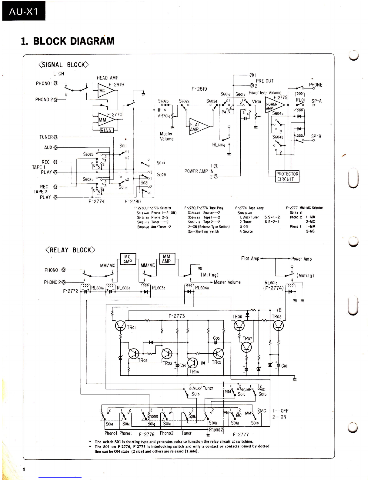
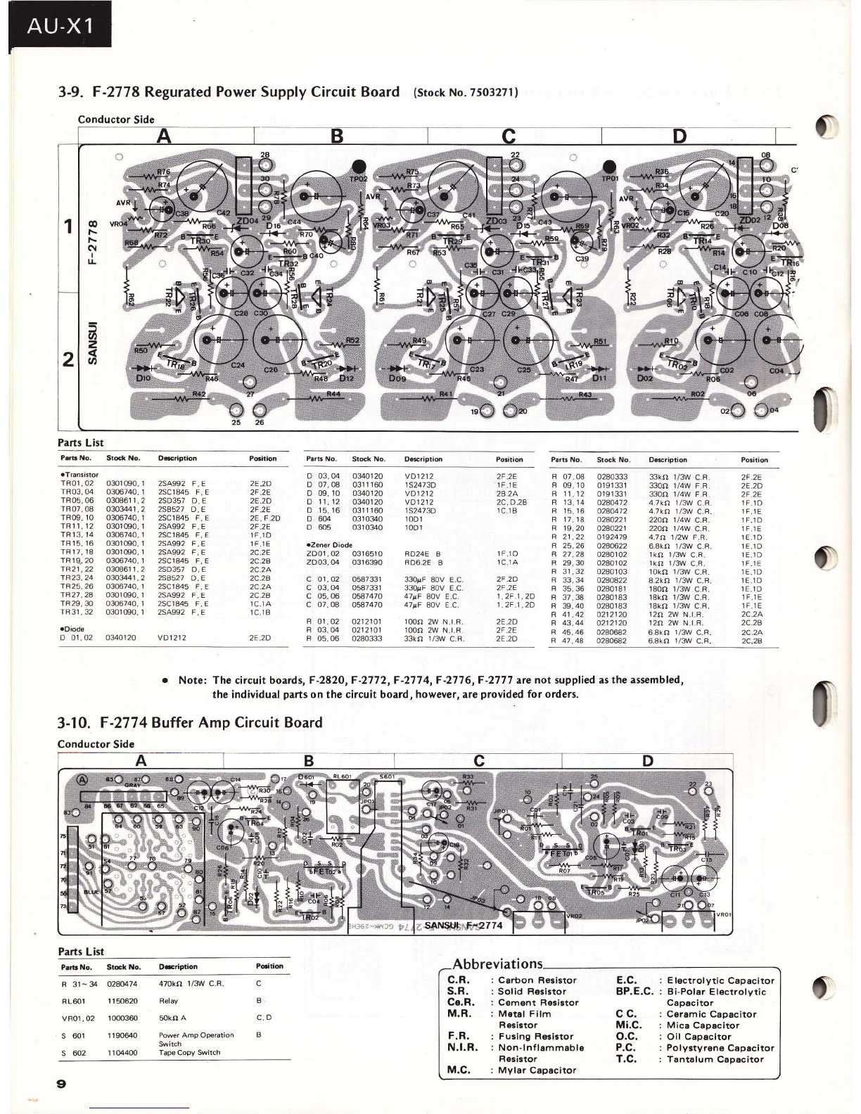
Sansui AU-X1 User manual

SUPER
I,
Nl'EGRA
TED
AMPLIFIER
SANSDI
AU-Xl
SANSUI
ELECTRIC
CO.,
LTD.
AU-X1
\
SPECIFICATIONS
Power
output
Min. RMS,
both
channels
dr
With no
more
tha~
0.007
%t "
~rmonic
distortion
160
watts
per
channel
into
8
ohms
Load
impedance
. . . . 8
ohms
.
Total
harmonic
distortion
(POWER
A},1P
IN)
. . . . . . .
....
less
than
0.007
%
at
or
below
rated
min. RMS
power
output
Intermodulation
distortion
(70
Hz : 7 kHz =4:1 SMPTE
method)
(POWER AMP IN)
less
than
(j.007 %
at
or
below
rated
min
:·
.RMS
power
output
Risetime
...
0.5 .
.Slew
rate
FreqlJ'ency response
(at
1
RIAA curve
deviation
(PHONO,
20
Hz
to
20
kHz)
..........
+0.2
dB>
...
0.2
dB
Input
sensitivity'and
impedance
(·1
kHz,
for
rated
power
output)
PHONO (MC)
....
0.1
mVt200
ohms
(Max.
input
capability:
40
mV
at
1
kHz,
le
ss
than
0.0
I %
total
harmonic
distortion)
PHONO (MM)
...
'2.5
mV/41
kilohms
(Max.
input
capability:
330
0.01 %
total
harmonic
AUX/TUNER,
TUNER,
POWER AMP
IN
.,
1
Output
level
and
impedance
(1
TAPE
REC . .
200
mV
into
47
kilohms/
600
ohms
PREAMPOUT
1 V
into
'
47
kilohms/
600
ohms
Channel
separation
(1
kHz,
at
rated
power
output)
PHONO (MC)
..
.
70
dB
PHONO (MM)
...
75
dB
AUX/TUNER,
TUNER,
TAPE
PL~
V
y
. . . . . . .
80
dB
Hum
and
noise
(short-circuit,
A.n~tWork)
PHONO
(MC) . . . .
76
dB . .•.
».
PHONO (MM)
...
91
dB;;;
'
AUX/TUNER,
TUNER,
TAP£pLAY
........
10QdB
Controls
SUBSONIC . . . - 3 dB (
16Hz),
6
dB/oct
J!JMP
..
.
..
. -
14dB
Power requirements
Power
voltage
....
100,120,220,240
V
(50/60
Hz)
Po~er
consumption
Rated
consumption
500
watts
Dimensions
480
mm (18-15/16") W
197
m
'11
(Z:13/16") H
450
,rnm
·3/4
H)
D
27.7
k '
lbS)
net
30.4 k )
packed
* Design and
specifications
5U~,ect
to
c.hanges
without
notice
for
improvements.

1.
BLOCK
DIAGRAM
<SIGNAL
BLOCK)
L-CH
AUX@~------------~
REC
@
SOl
i
Master
Volume
SOlO
TAPE
I
----+-+-
-
---'=e=+~=t=t_
PLAY
@----
S02e
REC
@'--~j--
-
--::1
TAPE
2 .
____
L~======:::'J
PLAY
@----
<RELAY
BLOCK)
PHONO
I@;---....,
PHONO
2@;------='
__
_
F-2780
F-2780,
F-2776
Seleclor
SOIl.-d)
Phono
1···210NI
Soil.·,)
Phooo
2···2
5011
'.1)
Tun
...
--'--2
SOllm.p)
Au~/Tuner--2
F-2772
+-D4----+
......
'-------+-.H
S6010
S601
b
I
@'-------'
POWER
AMP
IN
2@'--
-----l
@I
PRE
OUT
@2
F'2780,F-2776
T~
Ploy
So2I,·d)
Source
···-2
So21.·hI
Tape
1,---2
50211-1)
Tope
2-",2
2-·-QN
IReleose
Type
Swilch)
Sol--Shorling
Swilch
F-2774
Tape
Copy
S602I,·d)
I.
Au~!Tun",
5.5-1-2
2.
Tuner
6.
5-2-1
3.
Off
4.
Source
(
Muting)
__.L.--~·-Moster
Volume
RL6040
'--------------«1
~
AuxlTuner
SOlo
PHONE
0--------<)
SP-A
SP-B
F'
2777
MM
MC
Seleclor
SOII,·DJ
Phano
2
I···MM
2-·MC
Phono
I
I-'MM
c·MC
I···
OFF
2
ON
• The switch SOl
is
sharting
type
and generates pulse
to
function
the
relay circuit at switching.
• The
SOlon
F.2776, F-2777
is
interlocking switch and only a contact
or
contacts joined by
dotted
tine can be ON state (2 side) and others are released
(1
side).
u
u

AU-X1
2.
THE
OPERATION
&
CHARACTERISTIC
OF
HIGH
SPEED
POWER
TRANSISTOR
In
order
to
up-grade
the
sou
nd
quality,
AU-Xl
employs
the
cir-
cuitry
of
the
push-pull
drive
DC
comfiguration
from
MC
head
amp
to
po
'
wer
amp
stage, which provi
de
superior
dynamic
and
open-loop
characteristics
.
The
improvement
was
made
for
parts
such
as volumes, wires, relays,
electrolytic
capacitors
and
semi-conductors.
In
particular
, newly
developed
linear high speed device, LAPT
(Linea
r
Ampl
ifier Power
Transistor)
is
adapted
in
power
stage,
and
the
combination
use
of
this
high speed
power
transistor
and
diamond
differential
circuit
allows slew
rate
of
260
V
Ills
and
wide range low
distortion
amplifi-
cation
.
2-1. High Speed Power Transistor
The
requirements
for
power
trnasistor
in
order
to
elevate
sound
quality
are;
*
to
have high cut'<lff
frequency,
fT
(high speed device).
*
to
make
voltage
dependance
of
DC
forward-current
transfer
ratio,
hFE
be little and have
excellent
linearlity.
*
to
have a large
A.5.0.
(Area
of
Safe
Operation)
and
strong
en-
durance
against
break-down
.
The
use
of
high speed
power
transisto
r
with
requirements
above
together
with
circuit
improvement
is
effective
for
achievement
of
wide range and low
distortion
'
amplification
.
Transistors
to
meet
with
these
requirements
are
both
bi-polar and field
effect
transistor
(FET).
Note:
Cut-off
frequency,
fT
shows
the
frequency
at which
the
small signal
current
gain will be 1
(0
dB) in
common
emitter
circuit.
Comparison between bi-polar and field effect type as power
transistor.
Table
1;
Comparison
of
bi
-
polar
and field
effect
type
as a
power
device.
Field
effect
Characteristics
Bi-polar device
junc
-MOS
FET
type
tion
type
FET
SIT
Input
impedance
low high high
Thermal
coefficient
of
positive negative negative
operating
current
StOlied carrier
effect
exist
none none
(Carri
er
strage
effect)
Transfer
character
istic
exponential
square
square
Idring
current
as a little large large
output
device
Output
characteristic
pentode
triode
pentode
State
at
no
input
bias
off
on
on
Current
path
(Channel) vertical vertical vertical &
horizontal
Threshold
voltage low inter- high
mediate
Cost low high high
The
advantages
of
FET
are high
input
impedance
and no
thermal
run-away because
of
negative
thermal
coefficient
of
operating
cur·
rent
however
there
still
remains
price
problem
on
FET,
in
addition,
bi-p~lar
type'
high speed
power
transistor
are variously developed
and
becoming
common
so
that
AU·X1
employs
bi-polar
type
power
trnasistor
(LAPT).
2-2.
The
Configuration
of
High Speed Transistor
In
order
to
increase
the
cut-off
frequency,
fT,
it
is
necessary
to
make
transistor
base as
thin
as possible,
but
it
oppose
to
A.S.O.
(Area
of
Safe
Operation)
to
enlarge. When
making
the
transistor
base
thill,
the
injected
current
density
is increased so
that
junction
is
destroied
by
second-breakdown.
To
solve above
problem,
the
con-
struction
of
power
trans
i
stor
(LAPT)
is
parallel
connection
of
devided 35
of
small signal
transistors,
in
addition,
the
defusion
resistor
is
made
at
each
emitter
of
devided
transistor
to
equalize
the
flowing
current.
Fig. 1
Illustration
of
emitter
ballast
resistor
made
by
defusion.
B
ase
emitter
n"
Fig.2
Equivalent
circuit
of
ballast resistor
defused
to
emitter
of
transistor.
"
r§
"'
1COllecto
r
Ba
se
b
all
ast resistor
,
..
/ (
de
f
fusi
on
res
istor)
... emitter
Fig. 3
Surface
of
LAPT
before
evaporation.
e
mitt
er contact
I
By
connecting
many
small signal
transistors
with
high fT in parallel,
power
transistor
with high fT and large A.S.O. can be
obtained.
If
there
is
current-concentration
to
one
of
small signal
transistors,
the
voltage
between
emitter
and base
is
decreased
by
the
ballast
resistor
(deffusion
resistor)
at
emitter,
which causes
internal
negati~e
feedback
and relieves
the
current-con~entration.
2-3.
The
Characteristic and Merit
of
use
of
High
Speed Power Transistor
•
The
relation
between
switching
time,
fT,
and
hFE
of
power
transistor.
Fig.4
Switching
time
i
np
u
t
~
: :t
st
~
-- d
ON
t--
--
1,1
-I
t 1
~
I-
t l 0
Qu
tputwavefo
rm-
,
-
~-----:-:-
-
-T
lOYo
: : I
90%
Fig. 5
Influence
of
switching
time
against sine-wave
(of
half
cycle)
~
,_t
s
~g
..
ton
........t
urn-ont
ime l
tON I \
tt
I
..
" \ : ".. tf ··.. ··
··f
a
ll
t
im
e _ switching time
.J
..
~
..
tstg ·······
·st
orage t
im
e
The
more
the
switching
time
is
shortened
(high speed)
the
more
the
frequency
range
characteristic
of
power
transistor
is
improved;
this
relation
is
indicated in Fig.
4),
5).
Fig.
6),
7),8)
show
the
more
the
fT
is
raised
the
more
the
switching
speed
is
quickened.
2

i
AU-X1
• The relation between switching time, fT and
hFE.
(x,
ll,
0,.
showing
the
quantity
of
transistor & distribution)
10 Fig. 7
Fig. 6 (NPN)
50
tstg- h
FE
(NPN)
30
i
20
'il.
2
~
.;:;
~
10
0.5
3
0.3
10
30
50
lOO
300
IM
3M
5M
hFE(5V/IA)
Next,
the
following Figs show
that
the
relation between high fT
of
power transistor and short periode
of
tstg influences the improve-
ment
of
distortion (THD) effectively
in
audio amplifier.
Fig.
9),
10)
show
the
THD becomes
better
when tstg
is
faster.
Fig.
11),
12) illustrate
the
relation between
output
current wave-
form
of
emitter
and distortion wave-form. From these Figs, it
is
• OutPl,lt wave-form & distortion wave-form near
at
clipping point.
O.l%range
IOV/div
Fig.9
T.H.D. 0.
1%
tstg =
1.6,us
I
switching distortion
• Wave-forms
of
emitter
current and distortion
(condition)
Po~
40W
Fig.
11
RL
~
8fl
.-
f ~
50KHz
lE
wa
veform(
NPN
)
2A/DIV
lEwaveform(PNP)
monitor
wav
eform of
distortion meter
0.1
%range
O.5V/div
T.H
.
D.
0052%
fT(NPN/PNP) = 4.0/8.0MHz
N
PN
tf-
IT
Fig
. 8
tON
-
fT
1.0
(NPN)
0.5
\
!
0.3
5 0.2
0.1
0.05
IOM
30
M
50
M
lOOMz
IM
3M
5M
IOM
30M
SOM
lOOMz
fT(5V/IA) fT(5V/IA)
obvious when the fT
of
power transistor
is
low
the
output
current
wave-form becomes dull, and
the
switching function
at
B class push-
pull operation
is
not
performed precisely.
These above
phenomenon
causes
the
increase
of
ope
rating current
and deterioration
of
distortion.
Fig.
10
T.H.D.
0.035%,
ts
tg
=0
.
5,us
Fig.
12
T.H.D.
0025%
fr
(NPN/PNP) = 30/21MHz
N
PN
d\A}
v
~
L-
__
___
3
______
____________
______
__________
______
__
________________________________________________
~

3.
PARTS
LOCATION
&
PARTS
LIST
3-1. F-2917 MC
Head
Amp
L-CH Circuit Board (Stock No.
7551421)
3-2. F-2918
MC
Head
Amp
R-CH
Circuit Board (Stock No.
7551431)
Conductor
Side A
J
POl
B
1
2
R50
SANSUl
F-29H
~
'
PRl
~)
('
3
'"
U
Since
some
of
capacitors and resistors are
omitted
from parts lists in this Service
Manuai, refer
to
the Cornmon Parts List
for
capacitors
& resistors which was
appended
previously
to
each Sansui Manual.
Parts List
Parts
No.
Stock
No.
Description
Position
_Transistor
F·29
17
F·2918
TROl
0301090
.
2SA992
F.
E
28
4A
TR02
0306740.
2SC1845
F.
E
2A
48
TR03
0306740.1
2SC1845
F.
E
18
3A
TR04
030
1
090.
1
2SA9
92
F.
E l A
38
TR
05 0
3067
4
0.
1
2SC1
84
5
F.
E
18
3A
TR06
030
1
090.
1
2S
A992
F.
E
lA
38
TRG7
0308501.2
2SD
35
7
D.
E
18
3A
TR08
0303331
. 2
2S8527
D.E
lA
38
.FET
FETOl
-
02
03
7
0344
- 7
2SK163Ml.
M2
.
Nl.
N228
4A
FE
T08
-14
0370334
- 7
2SJ44Ml
<
M2,
N l ,
N2
2A
48
.V
a
ristor
D 0 1
03
40170
MV
1
03
18
3A
D
02 03
4
0170
MV
1
03
18
3A
C 01
0622102
1000pF
125V
P.C.
28
4A
C 04 0581014
O.047j.iF
400V P,C.
iA
3A
C
10
0622102
1000
pF
125V
P.C.
18
3A
C
11
0622
1
02
1000pF
125V
P.C.
lA
38
C 12
0623300
30p
F
125V
P.
C,
18
3A
C 13
0623300
30pF
125V
P.C.
lA
38
C 14.16
0602109
l
/-l
F
100V
M.C
18
3A
C 17
0622
1
02
lOO
Op
F 125V P,C.
C
25
-29
06810
18 O.
22
1J
F M.C.
R
01
0280221
220
n 1!3W C.R.
28
4A
R
02
0280109
1n 1
/3W
C,R.
28
4A
R
03
0280109
1n
1!3W
CR
.
28
4A
R
04
0280109
In
1!3W C.R .
2A
48
R
05
0280109
1n
1!3W
CR
.
2A
48
R
06
-19
0280569
5.6n 1!3W C.R.
2A.8
4A.
R
20
0280224
220k
n
1!3W
C.R.
2A
48
R
22
0280120
1
2<2
1
!3
W
CR.
28
48
R
23
0280120
12n 1
!3
W C.R.
2A
4A
R
26
0280151
1
50
n
1!3W
C.R.
28
4A
R 27
0280151
150
n 1
!3W
C.R.
2A
48
R
28
0280101
lOOn
1!3W
CR.
28
4A
R 29
0280101
lOon
l!3W
CR
.
2A
48
R
30
.
31
0212150
15n
2W N.
I.R
.
28.2A
4A.48
R 34
0280561
560n
1!3W
C.R.
18
3A
R
35
0280511
510
n
l!3W
C.R
lA
38
R 36
0280224
220k
n
1!3W
C.R.
28
4A
R 37
028022
1
220
n 1
!3
W C.R. 18
3A
R
38
028022
1
220
n 1!3W C.R. l A
38
R
39
0280479
4.
7n
l!3W
C.R.
lA
38
R
40
0280
1
52
1.
5k
fl: 1
/3W
C.A.
18
3A
R
41
0280152
1.5kn 1
!3W
CR
.
lA
38
R
42
0280391
390n
1!3W
C.R.
18
3A
R
43
0280391
390n
l!3W
C.R. l A
38
R
44
0280479
4.7n
1!3W
C.R.
18
3A
R
45
0280479
4.
7n
1!3W
C.R. l A
38
R 46
0210478
0.4
7n
1!2W
N.I.R.
18
3A
R 47
0210478
0.47
n 1
12
W N.I.R.
lA
38
R
48
028010
1
lO
on
1!3W C.R.
R
49
0280221
220
n 1
!3W
C.R.
28
4A
R
50
0280824
820k
n:
l/3W
C.R.
VROl
1033570
1
DOn
B Center l A 38
DC
DV
Adj.
4

AU-Xl
3-3. F-2770 Equalizer Amp L-CH Circuit Board (Stock No.
7551441)
3-4. F-2771 Equalizer Amp R-CH Circuit Board (Stock No.
7551451)
tl'
Conductor Side Parts List
Par
ts
No
. Stock No. Description Position
e
Tr
ansis
tor
F·2770
F·2771
TR01
0306740.
2SC1
845
F. E
2A
48
TR02
0306740
. 2SC1845 F. E
2A
48
TR03
0301090.
2SA992
F.
E
2A
48
TR04
0306360.
2SC1
95
1-1, 2
2A
48
TR05
0306740.
2SC1
845
F. E
28
4A
TR06
0306740
.1
2SC1
845
F. E
18
2A
TR07
0306740.1
2SC1
845
F. E
28
4A
TR08
0306740
. 1 2SC1
845
F,
E
18
3A
T
R09
030
1
090
. 1
2SA992
F. E
2A
48
TR
10
030
1
090
.1
2SA992
F.
E
lA
38
T
R"
030
1
090.1
2SA992
F. E
2A
48
T
R12
030
1
090.1
2SA992
F. E
lA
38
TR13
0300760.2
2SA917·1.2
18
3A
TR14
0306360.
1 2SC1951·1
.2
l A
38
TR15
0306740
. 1
2SC
1
845
F.
E
18
3A
TR 16
030
1
090.1
2SA992
F. E
lA
38
T
R17
0308501.2
2SD357
D.
E
18
3A
TR18
0303331.2
2S8527
D.E
lA
38
-F
ET
FET0
1 0370321 2SK131
L.M
2A
48
-
Di
ode
D
01
03
1
0480
SV03
2A
48
D 02
0310480
SV03
28
4A
D
03 03
1
0480
SV03
18
3A
- Zener
Di
ode
ZD01
03
1
6570
RD33E 8
28
4A
C
01
0622
151 150pF
125
V
P_e.
2A
48
C
02
0623200
20pF
125V
P.C
2A
48
C
03
068
1014 O.047/.lF
400
V
M.C
2A
48
C
05
068
1014 O.
047J,LF
400V
M .C.
28
4A
C
07
0622362
3600pF
125V P.C.
28
4A
C
09
0623300
30pF
125V
PC
18
3A
C
10
0623300
30pF
125V
p.c.
lA
38
C "
068
1014
0
.
047~F
400
V
M.c.
18
3A
C
13
0622102
1
000pF
125V
P.C.
18
3A
C 14
0622102
1
000pF
125V P.
C.
lA
38
C
15
0623200
20pF
12
5V
PC
18
3A
C
16
0623200
2
0pF
125V
p.c.
lA
38
C 19
068
1001 O.47
/.lF
250V
M.C.
28
4A
C
20
068
1001
OA7~F
250V
M.c.
2A
48
C
23
0681001 0.47I-lF
250V
M.C 18
3A
C 24
0622332
3300pF
125V
PC
28
4A
C
25
0682037
0
.
12~F
100V
M.C
2A
48
C
26
0682023
O.
033/J.F
1DOV M .C.
2A,
B
48
C 27
0622202
2000pF
125V
PC
28
4A
R 01
0280563
56kn
1/3W
CR
2A
48
R
02
0280330
33n
1/3W
CR.
2A
48
R
03
0210182
1.8kfl
1/
2W
N .I
.R.
2A
48
R
04
0280333
33kn
1/3W
CR
.
lA
38
R
05
0280564
560kn
1/3W C.R
lA
38
R
06
0280103
10kn
1/3W
CR.
2A
48
R 07
0231182
1.8kn
1I
2W M.R.
28
4A
R
08
0231182
1.
8kn
l!2W
M .R .
28
4A
R 09
0280470
47n 1/3W
CR.
28
4A
R 10
0210102
lkn
1/2W
N.I.R.
28
4A
R
11
0280393
39kn
1/3W
CR.
2A
48
R 12 0280821
820n
1/3W C.R.
18
3A
R 13 0280101
lOOn
1I3W
CR.
28
4A
R 14 0280821
820n
1/3W
CR.
18
3A
R
15
0280101
lOon
1/3W
CR.
28
4A
R 16 0280101
lOon
1/3W
C.R . 18
3A
R 17
0280
1
51
150n
1/3W
CR.
18
3A
R 18
028015
1
150n
1/3W
CR.
18
3A
R
20
0280330
33n
1
/3W
C.R. l A
38
R
21
0280
1
51
1
50n
1/3W
CR.
l A
38
R
23
0280151 1
50n
1/3W
CR
. l A
38
R 24
0280
1
01
lOOn
1/3W C R.
2A
48
R
25
0280
101
lOOn
1
/3W
CR
. l A
38
R
26
028082
1
820n
1
/3W
CR
.
2A
48
R 27
0280
101
lOOn
1
/3W
C.R. l A
38
R
28
028082
1
820n
1
/3W
CR.
l A
38
R 29
0280
121 1
20n
1
/3W
CR.
18
3A
R
30
0280393
39kn
1/3W C.
R.
28
4A
R 31 0
28
0393
39kn 1/3W C R.
lA
38
R
32
0
280
121
12
0n
1
/3W
C.
R.
lA
38
R 33
0280
121 1
20n
1
/3W
CR.
lA
38
R 34
028039
1
390n
1/3W
C
.R
.
18
3A
R
35
028039
1
390n
1
/3W
CR.
l A
38
R
36
028033
1
330
n 1/3W
CR.
18
3A
R 37
028
0
33
1
330n
1/3W
C.R.
lA
38
R
38
0280
1
80
1
8n
1/3W
CR.
18
3A
R
39
0280
1
80
1
8n
1/3W
CR.
l A
38
R 40
028056
1
560n
1
/3W
C R.
28
4A
R 41
028
0
104
1
00kn
1
/3W
C
.R
.
28
4A
R
42
0280330
33n
1
/3W
CR
.
2A
48
R
43
028
02
29
2.2n
1/3W
CR
2A
48
R
44
023
1
203
20kn 1
/2W
M.R.
28
4A
R
45
023
1
682
6.a'n
1
/2W
M.R.
28
4A
R
46
0231 182
1.
8W
1/2W M.R.
2A
48
R
47
023
1391
390']
1/2W M
.R
.
2A
48
R 48
028
0
33
0 3
3n
1
/3W
C R. l A
38
VR01 1
033
890
4
700
B Center 28
4A
DC
OV
A
dj
.
5

3-5. F-2819 Flat Amp Circuit
Board
{Stock No. 7562781}
Conductor Side
~
P=art~s~L~is~t~
___________________________
Parts
No
. Stock No.
eTransistor
TR01.02
TR0
3.04
TR05.06
TR07.08
TR
09.10
TRll
. 12
TR
13.14
TR 1
5.16
TR
17.18
_FET
FET01.02
_Diode
0301090
0306740.1
0306740.1
0306740
0301090
. 1
0300760.1
0306360.1
0306360.1
0300760.1
0370361.2
D
01
.02
03
1
6390
D
03
.04
03
16390
D
05.06
0311160
D
07.08
0340150
D
601
.602 0310340
C
01.02
C
07.08
C
09.10
C
13.14
C 15. 16
C
25.26
C
27.28
C
29.30
C
31.32
R
01.02
R
03.04
0623300
0622152
0623100
068
10
14
0623309
0681018
0681018
0681001
0681018
0280101
0280823
Description
2SAG92 F. E
2SC1845
F.E
2SC1845
F.E
2SC1845
F.E
2SA992 F. E
2SA917·1. 2
2SC1951 ·1
2SC1951 ·
1.2
2SA917·1. 2
UPA68H L
1.
L2
RD6.2E 8
RD6
.
2E
8
lS
2473D
MV·12
10Dl
30pF
125V
P.C.
1500pF 125V P.
C.
lOpF
125V
P.C
.
0.047~F
400V
M.C.
3pF 125V P.C.
O.2~F
400V
M.C.
O.22~F
400V
M.C
0.47~F
25
0V
M.C.
'
0.22~F
400V
M.C.
l
oon
1/
':N>I
C.A.
82kn
1/3W
CR
.
Position
3.5
3.5
3.5
2.5
2.4
2.5
2.4
2.4
2
.4
3.
5
3.6
2.4
3.5
2.5
1
3.5
3.5
2.4
2.4
2
.4
2
.4
2.4
2.4
6
3.5
3.5
Parts
No.
Stock
No
.
R
07.08
R
09.10
A
13.14
R
15.16
R
17
.18
R 19.20
A
21.22
R
23.24
A
25.26
R
27
.28
R 29.
30
R 31. 32
A
33.34
R
35.36
R
37.38
A 39.40
R
41.42
R
43.44
R
45.46
A
47.48
R
49.50
R
51.52
A
53.54
R
55.56
R
57.58
A 59 -62
VR01.02
S 602
604
0280
104
0280823
0280562
0280821
0280222
0280102
0280103
0280470
0280470
0280152
0280222
0280331
0280222
0280222
0280272
0280272
0280681
0280681
0280151
0280822
0280820
0280820
.
0280
154
0280221
0280824
0280224
1034150
1131810
1190640
3-6. F-2773 Muting Circuit
Board
{Stock No.
7597401}
Conductor Side
r\
L
~
Parts
List
Parts
No.
Stock
No.
Description
Position
Parts
No
.
Stock
No
.
_Transistor R
03
0280101
TROl
0305951 . 2 2SC945 Q. P
18
R 04 0280472
TR02
0305951 , 2 2SC945 Q. P
28
A
05
0212220
TR03
0305951.2
2SC945 Q.P
18
R
06
0212152
TR04
0305951.2
2SC945
Q.p
28
R 07
0280333
TR05
0305
95
1.2
2SC945
Q.P
2A
R
OB
02B0473
TR06
0305951 . 2 2SC945
Q.p
18 R 09 02B0472
TR0
7 0305951 , 2 2SC945 Q. P
18
R 10 0280561
TR08
0305951 . 2 2SC945
Q.P
lA
A
11
0280183
R 12 02B0223
eDiode R
13
0280222
D
01
0310340
10Dl
lA
A
14
0280682
D 02
0311160
lS2473D
18
A 15 02B0223
D
03
0311160
lS2473D
lA
A
16
0280273
A
17
0280222
_Zener Oiode A
18
0280101
ZDOl
0316520 RD24E C
28
A
19
0280221
ZD02
0316290
AD12E 8
2A
A 20 0280471
ZD03
0316520
RD24E C
2A
R
21
0280123
ZD04
0316520
AD24E C
lA
A 22
0280153
R 23 0280101
R
01
0280101
loon
1/':N>I
C.A.
18
A 24 0280472
R 02 0280471
470n
1/3W C.A.
18
R
25
0280101
Description Position
l00kn
1
/':N>I
C.R . 3.6
82kn
1/':N>I
CR.
3.5
5.6kn
1/3W
CR.
3.5
820n
1/3W C.R. 2.5
2.
2kn
1/3W
CR.
3.5
1
kn
1/
':N>I
CR.
3.5
lOkn
1
/':N>I
C.R. 3.5
47n
1/3W C.R. 3.5
47n
1/3W
CR.
3.5
1.5kn
1/':N>I
CR.
3.5
2.2kn
1/
3W
C.R . 3.5
330n
1/3W C.R. 2.5
2.2kn
1/3W
CA.
2.4
2.2kn
1/3W C.R. 2,4
2.
7kn
1/
':N>I
CR
. 3.5
2.7kn
1/
':N>I
C.R.
3.5
680n
1/':N>I
C.R. 2.4
680n
1/3W C.R. 2.4
150n
1/3W
CR.
2.4
8.2kn
1
/':N>I
CR
. 2.4
82n
1/
3W
CR.
2.4
82n
1/3W C.R. 2.4
150kn
1/':N>I
CR.
1.4
220n
1/3W C.R. 1.4
820kn
1/':N>I
CR.
6
220kn
1/
':N>I
CR
.
loon
B
Cente
r
DC
QV
Adj. 3.5
Jump
& Subsonic
Filter Switch
Speak.ers S
wi
tch
(
~
<)
Description Position
lOOn
1/3W
CR.
28
4.7kn
1/':N>I
CA
.
18
22n
2W
N.I.R.
2A
1.5kn
2W
N.
I.R.
18
33kn
l/3W
C.R .
28
47kn
1/3W
CR
. 18
4.7kn
1/3W
CR
.
18
560n
1/3W
CR
.
28
18kn
1/3W C.R . 18
22kn
1/3W C.R
28
2.2kn
1/3W
CR.
18
6.Bkn
1/3W
CA.
2A
22kn
1/
3W
C.A. l A
27kn
1/3W C.R .
2A
2.2kn
1/3W C.A.
lA
lOon
1/
3W
CA.
18
220n
1/3W
CR.
18
470n
1/
3W
CR
.
lA
1
2kn
1/3W
CA
.
2A
15kn
1/3W
CA.
lA
loon
1/
3W
CA
.
4.7kn
1
/':N>I
CA.
lA
lOon
1/':N>I
C.R.
lA
8
J

AU-X1
3-7. F-2775 Driver Amp Circuit
Board
(Stock No. 7572191)
Conductor
Side
1
2
3
Parts
List
Parts
No
. Stock No.
Dncription
Position Parts
No
. Stock No. Oescription Position Parts
No
. Stock
No.
Dea:ription Position
eTransistor C
04
0681013
0.
033.F
400V
M.C
l C R
23
0280121
120n
1/
:]#
C.R. l B
TROl
0306680.1
2SC2071
B.
V
lA
C 07
0681013
0.
033
.F
400V M.C. l C R 24 0280121
120n
1/
3W
C.R .
lB
TR02
0306740.1
2SC1845 F. E
lC
C
09
0623309
3p
F 125V P.C.
2C
R 25
028010
1 lOOn 1/3W C.R .
lB
TR03
0306740
. 1 2SC1845 F. E l C C 10
0623309
3pF
125V P.
C.
2B
R 26 0280101 lOOn 1/
:]#
C.R .
lB
TR04
0306740
. 1 2SC 1845 F. E
lC
C
11
0623109
lpF
125V P.
C.
28
R 27
028082
1
820n
1/
:]#
C.R .
lB
TR05
0306740.1
2SC1845 F . E
lC
C 12
0623109
lpF
125V P.C.
2B
R 28 0280821
820n
1/
:]#
C.R.
lB
TR06
0301090.1
2SA992
F. E
lB
C 13
0622102
1000pF
125V P.C.
28
R 29
0280393
39kn
1/
:]#
C.R .
2C
TR07
0301090
. 1
2SA992
F. E l B C 14
0622102
1000pF
125V P.C.
2B
R
30
0280393
39kn
1/
3W
CR
. 2B
TR0
8
0301090.1
2SA992
F. E l B C 15
0623330
33pF
125V
P.C
. 2C R
31
0280
151
150n
1/
:]#
CR
. 2C
TR09
0301090.1
2SA992 F. E l B C
16
0623330
33p
F 125V
P.C
2B
R
32
02B0472 4.
7kn
1/
:]#
CR
. 2C
TR10
0301030.1
2SA9
39
B.
V
2C
C 18
06
Bl0
13
0.033
.F
400V M
.C
.
2B
R
33
028068
1
680n
1/3W C.R .
28
TRll
0306680
. 1 2SC2071 B. V
2B
C 19
06810
18 0.
22
. F 400V M.C.
lA
R 34
0280
1
51
1
50n
1/
3W
CR.
2A
TR12
0
306740.
1 2SC1845
F.
E 2B C
22
0681018
0.
22
.F
400V
M.C
. l A R 35 02
80560
5
6n
1/
:]#
CR
. 2C
TR 13
0306680.1
2SC2071
B.
V 2C C
29
0622681
680pF
125V P.C.
lC
R
36
028039
1
390n
1/
:]#
C.R.
2C
TR14
0301030.1
2SA939
B. V
2B
C
30
0681014 0.
47.F
400V
M.
C. 3A R 37
028039
1
390
n 1/3W C.R. 28
TR15
03
06860
. 1 2SC2238LB O. Y 2C R
38
0280103
1
0kn
1/
3W
C.R.
TR16
0301020.1
2SA
968LB
O. Y
2B
R
39
021056
1
560n
1/
2W
N.I.R. 2C
TR 101
0306740.1
2SC 1845 F . E 3C R
01
0280104
1
00kn
1/
:]#
C.R.
lB
R
40
0210561
560n
1/
2W
N.I.R. 2B
R 02
02
8068
1
680
n 1/3W C.R . l B R
41
0210470
47
n 1/2W N.I.R. 2C
_FET
R
03
021 2272 2.
7kn
2W
N.I.R . 2C R
42
0210470
47n
1/2W N.I.R. 2B
FETOl 0370251 2SK97
lB
R
04 02
31
392
3
.9kn
1/
2W
C.R.
lC
R
43
02
1
0120
12n
1/
2W
N.I.R. 2A
eDiode
R
05
0231392
3.9kn
1/
2W
C.R.
lC
R
44
02
1
0120
12n
l/2W
N.
I.R. 2A
o
01
0310480
S
V03
lC R 07 0280471
470n
1/3W C.R.
lC
R
45
0280273
27kn
1/3W C.R.
lA
o
02
0310480
SV03
l C R
08
0280470
47n
1/
:]#
C.R.
lA
R
46
0207100
1
0n
7W
N.
I.R
. 3B
o
03
0310480
S
V03
2C R
09
02
80470
47n
1/
:]#
C.R.
lA
R 47
02
1
3392
3.
9kn
:]#
N.I.R.
3A
o
04
0310480
SV03
2B
R 10
0280470
47n
1/
3W
C.R.
lA
R
48
0213392
3.9kn
:]#
N.I.R . 3A
o
05
0310340
1
00
1 2C R
11
0280152
1.5kn
1/3W C.R.
lA
R 101
0280104
100kn
1/3W C.R. 3C
o
06
0310340
1
001
2B R 12
028033
1
330n
1/
3W
CR
.
lB
R 102
0280223
22kn
1/3W C.R . 3C
0 101 0
340150
MV12 3C R 13
0280392
3.9kn
1/3W
CR
. 2A R
103
0280680
68n
1/3W C.R. 3C
0 102 03111
60-
l
S24730
2C
R 14 0280101
lOOn
1/
3W
C
.R
.
lC
R 104
0280393
39kn 1/
:]#
C.R. 3C
0
103
031
0400
lN
34A
2C
R 15 0280101
loon
1/3W C.R .
lB
R 105 0
280222
2.2kn
1
/:]#
C.R. 3C
0 104
03
11
1
60
l
S24730
2C
R 16 0280821
820n
1
/3
W C.R .
lC
R 1
06
0280823
82kn
1
/:]#
C.R. 3C
R 17 0280821
820n
1/
:]#
C.R .
lC
R 107
0280822
8.
2kn
1/
:]#
C.R . 2C
_Zener Oiode R 18 0280101 lOOn 1/3W C.R . l C
ZD
Ol
03171
90
R0
2
7F
IBI
lC
R 19 0280101
loon
1/3W C.R .
lC
V
ROl
10
335
70
100n
B 2.5x2 Ce
nt
er
lA
Z0
02
0316310
RD13E B 2A R
20
0280
121 1
20
n 1/
3W
C.R.
lC
DC
OV
Adj.
C
01
0622101
100pF
125V P.C.
lB
R 21 0280121 1
20n
1/
:]#
C.R.
lC
VR
02
1
033630
l
kn
B 2.5x2
Bias
2B
C
03
062
3220
22p
F 125V P.C.
lB
R 22
0280820
82n
1
/:]#
C.R .
lB
Current Adj.
7

3-8. F-2781 Power Supply & Protector Circuit Board (Stock No.
7503261)
1
3
4
Conductor Side
(
.!V
A
~
~ ~
~
.;.
-I»
,0
66
6r(~
j
«2
I
o
",go
;"'1
'
r-
0
~T
+~
o
-u.
I (J1
'"
'"'
'"
'"
BLACK~I
__
~~
__
~
__
~
~
B
]
50
V
A
2
50
V
2A
2
5
0~
2A
c
EQ
.4
F0 2
o
Parts List
Parts
No
. Stock No.
-T
rans
istor
TR601
TR602
T
R603
TR604
TR605
TR606
TR607
TR608
-Di
ode
o
01.02
o
03.04
o
05.06
o
07.08
o
09.10
o
11
o 12
o 601
o
602
o 603
o 604
o 605
o
606
o 607
o
608
o 609
o 610
o
611
o 612
o 613
_Zener Oiode
030861 1.
030595
1.
0305951.2
0305951.2
0305951.2
0308611.2
0305951.2
0305951.2
0311700
0311160
0311160
0311310
031
1320
0311700
0311700
0311700
0340150
0311160
0311160
03
11160
0311160
0311160
0311160
0311160
0310340
0310340
03
1
1700
0310340
Z0601
0316510
Z0602
0316390
_seA
SCR601
C
03.04
C
05.06
C
07
C
08
C
09
C 10
C
11
C 12
C 601
C 608
R
01.02
R
03.04
R 601
R 602
R
603
R 604
R
605
R
606
R 607
R 608
R 609
R
610
R 611
R 612
R
613
R 614
R
615
R
616
R
617
618
R 619
R
620
R 621
RLOl
RL02
01
02
03
04
601
602
603
604
0350020
0606108
0606108
0606108
0606108
0548001
0548001
0548001
0548001
0606108
0606108
0280223
0135221
0210829
0210102
0280174
[)280334
0280104
0280393
0280330
0280472
0280183
0280102
0280330
0280330
0280473
0280682
0280474
0280104
0280104
0280474
0212152
0280121
0159160
1150430
1150360
0432240
0432240
0432240
0432240
0432220
04
32220
043
1320
0433290
Description
2So357
O. E
2SC945
Q.p
2SC945
Q.P
2SC945
Q.
P
2SC945
Q.
P
2S0357
o.E
2SC945
Q.
P
2SC945
Q.
P
R8152
lS24730
1S24730
SS5
SS5R
RB152
RB152
RB152
MV12
1S24730
1S24730
1S24730
1S24730
1S24730
lS24730
1524730
1001
1001
R8152
1001
R024E
B
R06.2E
8
2S
F656
0.1"F
250V
M.C
O.ljJF
250V
M,C.
0.1"F
250V
M.G.
0.1 " F
250V
M
.C.
4700"F
25V
E.C
4700"F
25V
E.C
4700jJF
25V
E.C.
4700"F
25V
E.C
0.1"F
250V M.G.
o
lJ..1F
250V
M.C.
22Hl
1/3W C.R
220n
5W
Ce.A.
B.2n
l W
NI.R.
lk!1
1/2W
N.I.R.
470kn
1/3W C.R
330kn
1/3W
CR
100k<1
1/3W
C.R
39kn
1/3W C.R.
33n
1!3W
CR.
4.7kn
1/3W
CR.
18kn
1/3W
CR
.
lkn
1/3W
CR.
33n
1/3W C.R.
33n
1/3W C.R.
47kn
1/3W C.R.
6.8kl!
1/3W
CR.
470kn
1/3W
CR.
100kn
1/3W
CR.
100k<1 1/3W C.R.
470kH
1/3W C.R.
l.5kn
2W
N.I.A.
120n
1/3W
C.R.
3.9n
ZOW
Ce.R.
Relay
Relay
AC Fuse
2A
250V
AC
Fuse
2A
250V
AC
Fuse
2A
250V
AC
Fuse
2A
250V
AC
Fuse
1A
250V
AC Fuse
lA
250
V
AC
Fuse lOA
250V
AC
Fuse
SA
lZ5V
AU-X1
Position
4C
4B
3B
3B
3B
3B
2B
2B
3A.1A
3B
3B
3B.2B
3A.2A
2B
lB
4C
3B
3B
3B
3B
3C
2C
2C
2B
3C
4B
1C
4C
4B
3B
3A.1A
2B
2B
lB
2B
1B
lB
lA
4C
1C
3C
3C
4C
4B
3B
3B
38
38
3B
38
38
38
38
38
38.C
28
2B
28
3B
28
2C
2C
4B
3C
4B
2C
2C
2C
1C
4C
1C
4A
4A.B
8

AU-X1
3-9.
F-2778
Regurated Power Supply Circuit Board (Stock
No.
7503271)
1
2
<Xl
t--
t--
N
I
u..
Parts List
Parts No.
eTransistor
TR 01.02
TA03. 04
TA0
5.06
TA07
.08
TA09.10
TA11
. 12
TA1
3
.14
TR 15.1 6
TR17.
18
TR H
!,
20
TR2 1, 22
TA23.24
TR25. 26
TR27, 28
TR29 ,
3O
TR3
1. 32
-Oiode
D 0'
.0
2
Stock
No
.
0301090. 1
03
06
740. 1
03
08
611
.2
0303441 . 2
03
06740.1
03
01090.1
0306740. 1
03
0109
0. 1
030
1
090.
1
0306740. 1
03086
11
.2
03034
41
.2
03067
40
. 1
0301090
. 1
0306740. 1
030
1
090
. 1
0340
'20
Description
2SA992 F. E
25C1845 F. E
25D357 D. E
258527 D. E
2SC1845 F. E
25A992 F. E
2SC1845 F. E
25A992 F. E
2SA992 F. E
25C1845 F. E
25D357 D. E
25
85
27 D. E
25C1845 F. E
25A
992 F. E
2
SC1
845 F. E
25A992 F. E
V
D1
2
.2
- - - 8
Position Parts
No
.
Stock
No
. Oescription Positi
on
D 03. 04
0340
120
VD
1212
2F
.2E
2E.2D D 07.
08
0311160 1S2473D 1F.
1E
2F.2E D 09 .10 0340120
VD12
12 2
8.2A
2E
.2
D D
11
.
12
0340120 VD
121
2 2C. D.28
2F
.2E
D
15.16
0311160 1
S2
473D 1C.18
2
E.
F
.2
D D 604 0310340 10D1
2F.2E D 605 0310340 10D1
1F
.1D
1F.
1E
_Zener Diode
2C.2E ZD01 .02 0316510 R
D2
4E 8 I
F.
l 0
2C
.2
8
ZD
03. 04 0316390 RD6.2E 8 le.1 A
2C
.
2A
2C
.
28
C 01. 02
05
87331
33O
~F
80V
E.
C.
2F
.2
D
2C
.
2A
C
03
.04 058
73
31
33
0~F
80V
E.C. 2F.2E
2C.
28
C
05
.
06
0587470
4 7
~F
80V
E
.C
. 1. 2F.1. 2D
l e .1A C 07. 08 0587470
4
7
~
F
80V
E.C l , 2F .l .
20
1
C'8
R
01
.02 0212101
.o
on 2W N.I.R . 2E.2D
R 0
3.0
4 0212101 100n
2W
N.I.
R. 2F.2E
2E.2D R
05
.06 0280333 33
kn
. /
3W
C.R. 2E.2D
Parts
No
. Stock No.
Description
Position
R 07
.08
02803
33 33
kn
1/3W C.R. 2F.
2E
R 09.
10
0191331 330n 1/
4W
F.
R.
2E
.2
D
A
11
.12
01
91
3
31
33
0n
1/
4W
F.A 2F
.2
E
A 1
3.14
0280472
47kn
1/
3W
CA.
1F.1D
A 15.1 6 0280472 4.
7kn
1/
:NV
C.A. 1F
.1
E
A
17
.
18
0280221 22
0n
1/4W
CA.
1F.1
D
A
19.20
02802
21
22
0n
1/4W C.A. 1F.1E
R
21.2
2 0192479 4.
7n
1/
2W
F.R. 1E.1D
R
25.2
6 0280622 6.8
kn
1/
3W
CR.
lE. l 0
R
27.28
0280102 n n 1/
:NV
C
A.
1E.1D
R 2
9.30
0280102
1kn
1/
:NV
C R. 1F.1 E
R
31
.32
0280
103 10
kn
1/
:NV
C.R. 1E.1D
R 33.34 0280822 8.2kn 1/
3W
C.R. 1E.1D
R 35.36 0280181 18
0n
1/
3W
C R. lE. 1D
R 37.38
028018
3 18
kn
1/
:NV
C.R. 1F.l E
R 39. 40
0280
1
83
18
kn
1/
:NV
CR
. 1F.
1E
R
4'
. 42 02.
2120
12n 2W N.I.R.
2C
.2A
R 43. 44
02
.2120 1
2n
2W
N.I.R. 2C.28
R 45.46
028
0682
6.8kn
1/
3W
CR
. 2C.2A
R 47. 48 0280682 6.
8k
n 1I3W
CR.
2C
.
28
• Note: The circuit boards,
F-2820, F-2772, F-2774, F-2776,
F-2777
are
not
supplied as the assembled,
the individual parts
on
the circuit board, however, are provided for orders.
3-10. F-2774 Buffer Amp Circuit Board
Conductor Side
Parts List
Parts No. Stock
No
.
D-=ription
Potition Abbreviations
31- 34
02
80474
470kn
1/
:NV
C.
R.
C C.R.
Carbon
Resistor
E.C_
Electrolytic
Capacitor
R S.
R.
Solid
Resistor
BP.E.C.
Si-Polar
Electrolytic
RL601 1150620 Relay 8 Ce.R.
Cement
Resistor
Capacitor
50kn
A C. D M.R.
Metal
Film
CC.
Ceramic
Capacitor
VA01.02
1000360
Resistor
Mi.C.
Mica
Capacitor
601
1.90640
Power
Amp
Operation 8 F.R.
Fusing
Resistor
O.C.
Oil
Capacitor
Switch N.I.R.
Non-Inflammable
P.C.
Polystyrene
Capacitor
602 1104400 Tape Copy Switch
Resistor
T.C.
Tantalum
Capacitor
M.C.
Mylar
Capacitor
9

Parts List
Parts
No.
Stock
No.
Desc
ri
ption Position
A
49
.50 0280471
470n
1/3W C.A.
28.2A
A
51
.52 0280471
470n
1/3W C.A.
2e.28
A
53.54
0280122
1.2kn
1/3W C.A. l
e.
1A
A
55.56
0280122
1.
2kn
1/3W C.A. 1e
.1
B
A
57.58
0280221
220n
1/3W C.A.
1.2C.1A
A
59:
60
0280221
220n
1/3W C.A. 1e.
18
A 61
.62
0192229
2.2n
1/2W F.A.
18.
1A
R
65.66
0280561
560n
1/3W C.R. 1
e.1A
A
67.68
0280102
1
kn
1/2W
e.A
.
lS.
l A
A
69.70
0280
1
02
1
kn
1/2W C.R. 1e.18
A 71
.72
0280392
3.9kn
1/3W C.A .
lB.1A
A
73.74
0280562
5.
6kn
1/3W C.R.
lS
.l
A
A
75.76
0280
1
03
1
0kn
1/3W C.A. 18.
1A
R
77.78
0280102
1kn
1/3W C.A . 1
e.18
VA01.02
1
033670
4.7kn
B DC
Volt
Adj.
lE.1D
VA03.04
1
033650
2.2kn
B DC
Volt
Ad
j.
lB.1A
3-13. F-2772 MC,
MM
Mother Circuit
Board
Conductor Side
3-14.
F-~776
Selector Switch Circuit Board
Conductor
Side
3-11. F-2820
Speakers
Relay Circuit
Board
Conductor Side
Parts List
Parts
No
. Stock No. Description
eDiode
D 01
.02
03
1
0340
lOD
1
C 01
.02
0681014
0
.
047~F
400V
M.C.
A
01.02
02
1
2109
1n 2W
N.I.R.
A
03
.
04
0207100
1
0n
7W N.I.A.
L
01
.02
4290370
RF
Coil l",H
AL01
.02
1150410
Relay
3-12. F-2777 MC,
MM
Switch Circuit Board
Conductor Side
SANSU,-
F-
2777
Parts List
Pa
rts
No. Stock No. Description
S 01
11
31830
S
02
11
31820
Se
l
ec
tor Switch
Tape
Pl
ay Switch
Parts List
Parts
No
. Stock No.
S
01
11
31
800
Parts List
Parts No. Stock No.
-Di
ode
D60
1 - 603
03
1
0340
C
60
1
C 602 0504471
0504471
AL601
-604
1150620
Description
MM/MC
Sw
itch
Description
lOD
1
470
~F
35V
EC
.
470
~
F
35V
E.
C.
Relay
AU-X1
Position
2B
1
A.2A
1B.2B
lA.2A
1
B.28
2A.2
B
Positi
on
A.C
C
B
A.B.C
10
I

AU-Xl
4. ADJUSTMENTS
Notes: 1. Level Volume . . . . . . . . . . . . . . Minimum
2. Room Temperature
.. ..
. . . . . . 18°C -28°C
(65° F -
83
°F)
3.
When
replacing
some
parts
or
circuit
board, refer
to
description in REMARKS.
4.
For
this adjustment, run the
unit
for
more than' 3
minutesafter the power
is
switched ON.
4-1. F-2778 Power Supply Voltage
Adjustment
(See
Top
View
on
page 12)
STEP SUBJECT MEASURE ADJUST ADJUST
REMARKS
OUTPUT
FOR
1
For
MC Head Between
GND
&
VR03
-10
.5
V
F·
2
778
AmpL-CH
TP01 F-2778
2 For
MC
Head
Between
GND
&
VR04
-10
.5 V
r--
(TPOl -TP04)
Amp
R-CH TP02 F-2778
ffi
3
For
MM Head Between
GND
& VR01 -
47
.5 V + -
Amp
L-CH TP03 F-2778
~
4 For MM
Head
Between
GND
& VR02
-47.5
V
Amp
R-CH TP04 F-2778 (Cha
ss
Is) •
4-2. F-2775 Driver Circuit
Adjustment
(See
Top
View on page 12)
STEP SUBJECT
1 DC
OV
Adj.
L-CH
2 DC
OV
Adj.
R-CH
3 Bias current
Adj
.
L-CH
.
4 Bias current
Adj.
R-CH
MEASURE
OUTPUT
Spe
aker terminal
Speaker terminal
Between emitters
of
power
transistors, TR701 &
TR70
3
(between T.P Pi
n)
Between emitters
of
power
transistors,
TR702
&
TR704
(between T.P Pin)
ADJUST
VR01
F
-2
77
5
VR01
F-
2
77
5
VR0
2
F
-2
77
5
VR0
2
F-2775
ADJUST FOR
REMARKS
DC
OV
±5
mV
Before
turning
ON power switch,
set
VR01
to
center position.
DC
25
mV
±1
mV
Before
turning
ON power s
witch,
turn
VR0
2
fully
counterclockwise.
This bias current adjustment con-
verts current value
into
voltage
by
Ohm's law.
4-3. F-2917, F-2918
MC
Head
Amp
Adjustment
(See
Top
View
on
page 12)
STEP SUBJECT MEASURE
OUTPUT
ADJUST ADJUST FOR
REMARKS
1 DC
OV
Adj.
Between GND & common VR01
DCOV±5mV
Before turning ON power switch,
set
L-CH F-2917
joint
of
emitter
resi
stors F-29
17
VR01
to
center position.
R41, R47 (TP01)
2 DC
OV
Adj
.
Same
as
above VR01
R-CH F-
291
8
F-
2918
4-4. F-2770, F-2771 Equalizer Circuit
Adjustment
(See
Top
View
on
page 12)
STEP SUBJECT
MEASURt
OUTPUT
ADJUST ADJUST FOR
REMARKS
1
DC
OV
Adj.
Between
GND
& common VR01 DC
OV
±50
mV
Before
ll!rning
ON power switch, set
L-CH F-2770
joint
of
emitter
re
sistors
R38, R39 (TP01) F-2770 VR01
to
center position.
2 DC
OV
Adj.
Same
as
above VR01
R-CH F-2771 F-2771
4-5. F-2819
Flat
Amp
Circuit
Adjustment
(See
Top
View &
Bottom
View
on
page 12)
STEP SUBJECT
MEASURE
OUTPUT
ADJUST ADJUST FOR
REMARKS
1 DC
ov
Adj
. Between
chassis
and
collector VR01
DCOV
±
5mV
Before
turning
ON power switch, set
L-CH connecti
ng
point
TP01
of
F-2819 VR01 &
VR02
to center position.
TR15
&
TR17
(Top View)
2 DC
OV
Adj.
Between
chassis
and
collector
VR02
R-CH connecting
point
TP02
of
TR
16 &
TR
18
(Bottom
View) F-2819
11

5. OTHER PARTS
5-1. Top View
Speaker Terminal
AC
Consent-~
:-·
VR01---
~~~~~~~~~~~~-~~
=_~
VR02----
~~-
~F_
~~~~~
~~
~
VR02------
-+
~~------
~
----~
1
VROl------
-r
--------------~
TP03·
VR01-
-
--l-
VR02--
---r
------------
--J
VR02(F·
2819)-------------------
--"
5-2. Front View
AU-Xl
~-·hround
Terminal
_____
--'-'l~
-
VR01(L·CH)
......r+
-+---VR01(R·CH)
VROl(L·CH)
VR01(R·CH)
TP01(R·CH)
--
-~
+-
-TP01(L·CH)
'-------
-+
-VR04(F·2778)
R01(F·
2819)
"'--l
~~~~!!!'!!!.'!:::"'=="'=~
-'
R03

5-3. Bottom View
R7
4P Terminal
INPUT Tuner/Aux
PRE
OUT
Tape Power AMP
IN
Parts
list
<Top
View, Front View & Bottom View>
Parts No. Stock No.
Description
Parts No.
-Transistor
11
TR701,702
0306890.1
25C2493
D. Y 12
TA703.704
0301200.
25A1068
D. Y 13
TA705.706
0306890.
25C2493 D. Y 14
TA707.708
0301200.
1 25C 1068 D. Y 15
TA709.710
0306890.
25C2493
D. Y 16
TA711.712
0301200.
25A1068 D. Y 17
18.20
C701 -
708
0559851 10000j.lF
BOV
E.C.
19
,21
C709 -712
0681033
1pF 250V M.C. 22
C
713.714
0559850
2200pF
100V E.C. 23
C
715
0659801
O.olpF
150V C.C. 24
A701 -712
0200479
47n
1/2W N.I.R
25
A713
-724
0159130
0.33<1
5W
Ce.A.
26
27
5006810
Bonnet
28
7008150
Front
Panel
Ass'y
29
J
5336600
Sansui Badge
30
0319090
LEO
)5152210
CS
Washer
7106150
Knob
Ass'y
5
1131790
Power
Switch
31
6
536740
Knob.
power
switch.
p
type
7
2430290
Phone Jack
8
1190640
Speakers
Switch
9
5319210
Knob.
speakers
switch.
Y-7
type
32
10
1000360
Left
Level
Volume.
50kn
33
Stock
No.
5319210
1000360
5319210
1190640
.
5319210
1090500
5319200
1131810
5326760
1104400
5319210
1131800
7106150
1131830
5326750
1131820
5326750
5396630
r426420
5426440
5396590
5396570
r426240
5426440
5396580
5059030
5517050
Voltage Selector
Description
Parts
No.
Knob,
level
volume,
Y-7
type
Right
Level
Volume,
50HZ
Knob,level
volume,
Y-7
type
Power
Amp
Operation
Switch
Knob.
power
amp
operation
switch
Volume,50kn
Knob,
volume,
X·7
type
Jump,
subsonic
switch
Knob,
jump
switch
Tape
Copy
Switch
Knob.
tape
copy
switch.
Y-7
type
MM/MC
Switch
Knob
Ass·y.
MM/MC
Switch
Input
Selector
Switch
Knob.
input
selector
switch
Tape Play
Switch
T701
Knob.
tape
play
switch
n02
4P
Guide
Plate
Ass'y
Indicator
Calor
Plate
4P
Guide
Plate
3P
Guide
Plate Ass'y
Indicator
F701
Color
Plate
3P
Guide
Plate
Bottom
Plate
Leg
Fuse
Holder
F701
~
Stock
No.
2450070
2230190
3800490
3910490
2230220
2230230
2200630
2200620
2200650
2200620
2200580
4002960
4002970
2410091
2410830
10432290
0434060
2300060
-4--'°709
Description
AC
Consent
Ground
Terminal
Power
Cord
705
706
702
715
Strain Relief, power cord
1P Speaker
Terminal
(Red)
1P Speaker
Terminal
(Black)
4P
Input
Terminal,
phono
shorting
type
4P
Input
Terminal.
aux/tuner,
shorting
type
4P Tape
Terminal.
non-shorting
type
4P
Power
AMP
IN
Terminal.
shorting
type
4P
PRE
OUT
Terminal.
non-shorting
type
Power
Transformer
Power
Transformer
Voltage
Selector.
Plug
Voltage
Selector.
Socket
5A 125V
AC
100V. 120V
lAC
lOA 250V
AC
220V. 240V Fuse
AC
F
use
Holder
12
-

A B
6. SCHEMATIC DIAGRAM 6-1.
Pre
Amp Section
CD
lUNER
AVX
13
HEAD
AMP
(MC)
___
_
f291i]
-
I
FETol
-o?
2SKI63
~
--
c
VRo
1
cenr
er
DC
DV
)£d
rus
t

AU-X1
E
T~3'
~_I
~--~
m
~
,,
----
2SA992
2SA917
Design and specifications subject to change without notice for improvement.
La
presentation et
,,,
~ifications
sont
susceptibles
d"t'r
modifi4M sans prtavis
par
suites d'ameliorations eventualles.
Anderungtn. die
dim
technischen FOrtschrltt dienen, bleiben \/orbehalten.
T
R/
5
2SCI845
TR17
2SD357(2.3)
TRM
2SA992
S
WITCHES
&;
C
ON
TR
OLS
5t.ltct
or(~
-277
6,
2780)
So/(
b-d)
P/tono}
'
501
(e
-11)
'
h.o
no 2
So,(i
-l
} T
uner
·
So/(
m-p
) A
ux
/run
er
Tape
Pl9
( F- 2776.27
80)
Soz
(a-d)
So
u
rce
·2
S02
(e-
h)
T
ape
I 2
Sozti
-l)
Tape 2 2
MM'MC Selector ( F-
2nn
'"
'"
'"
G'
~
!i:>
~
Sod
a-h
) Plwno 2 of,.,JfM,on-MC
SO!
(c
-d
) Phono I
ofN
.f"', on-MC
Jump{F
-2819)
56oz(
a-d
)
off,
on (-
l4dBl
Subsonic
(F-
2B
I9)
S
6oz(
a.
-h)
ofr,
on
(-
3dB
/16;:;)
Tape Copy ( F-
2774
)
S&o2(
a-d
) I. Aux
/T
uner
7.
Tun
er
3.
off
4. Source
5. S
-
/
~2
6.5-2
- 1
Puwer Amp
Oper
at
ion
(F-2774)
St;QJ{a~d)
I.
Integr
ated
TP
ol
"'
§
'"
&
02
2.
Exter
nal
in.
put
1. WC)
3 Ext
ernal
inpu
t
2.
(DC)
4.
Exterll.al
in
ut
2.
(AC)
F G
TRo3
.
05
.
07
TR
I3
,I5
2SCI845
2SC1951-1
(2)
~
~
~
~
02
H
PREOUT
~
1 .1
R
2
3
4
/3
5

A c o
6-2. Main Amp & Power Supply Section
DRIVER
------------------
IF-2?m--
~
,
~~~~.r=
==
==~n======r~====~
~==
~~;~~,==
~~~
~~==
==
=~~.r:[f==r,J~~======~----~~~--------~
2
=
SC
=
2~4=9=3~N
~
(O
~
Y
~
)
--------
~
=================
\Q
."
rH."
~
TN
70I,70?705}106,7(Jj,7lO '
~
01,".13
J'
~
TR
70J•
104
,707,
7IJ6,711,7!?
2SAI068N(O,Y)
2SC2238
(O,Y)
2SA968(O,YI
RD27F(BI
RDI2E(BI
00',02
SV
~
03
Do3,(J4
SV-03
005.06
100-1
-------------------
.
------------------------~
~?7751
~
-
~====~==~====~============~~~~====~~
__
____
__
____
__
-44+~
,
I
,
I
,
66
SYMBOL
6Ctramic
fi;I Styrol
@
Mylar
(B.
P1Bi
-PoII1TEl.tctrogtic
ElNon.
-
lnf/.Q~
Res
istor
•
~bJlFil1flk3istor
o
~m..ld
Rt3i.stor
III Fu..sing
Resistor
R.ESISTORS
Arrin
oizms,!3Watts,
1:
5%Tolerance
Unless other wise Notld.
K:k.f2
,M:M
l).
CAPACITORS
Are
in
pF,
Unuss
oterwise
Note
d,
P:pF
at
no
input
signal
TOLEliANCE
G;±Z,,",F:±I%
SWITCHES
Selector
[L
Phonc
I
F-2780
2.
Phono 2
lSola_pl
3.
Tu.ner
4.
Aux
7apePlay
[1.
Sou.rce
F
-27
80 1.
Ta.pe
-I
tsozCl-41
3.
To.pe
- 2
5peai<.ITS
[1.
off
F-2B
I.9
2. A
t~,*a,h)
3. 8
4.
A+8
~:::,b)
[!",
off
SPEAKERS
~
PIIONES
!
!.9OJ#W4JSO!iWlADJ
&th
channlll
OrivM
at
1kHz

-Xl AU-Xl
o.ign
and
specifications subject
to
changt without notice for improvement.
la
presentation
et
In
spk
ifications sont susceptibles d'.ter modifijes sans pr'avis
par
suites d'amilioration. Mntuel'
...
Anderungen. die
$m
technischen Fortschritt dienen, bl'iben vorbehalten.
F G
P
OWER
SUPPLY
:J:
O.22~
JAPAN Modq[
VI
,
27
Nu
01
~
,
,
~
~,
:G
~
:
,
,g
,
,
~
I
05
, ,
, ,
, ,
!&
,
iii
,
,
, ,
L_ _
...I
03
I
'Z
1:1
N",
, ,
I
..
t I
:J
_:
, ,
, ,
' ,
06
H
2SA917 2SA968
2SA992 2SC2238
2SC945 2S8527
cl
2SC1845 2SD357
2SC1951
~
1
ir
' '
.PA68HL
, M
~
2SJ44
2SK163
~
2SA1068N
2SC2493N
c~
2SK131
2SA939
2SC2071
I 2SK97
~
SI
D2G2S2
'c,
2
lN34A
lS2473D
RD6.2E
~+
~+
RD12E
RD24E
RD33E
RD27E
f~
MV12
MV103
lOD
1
VD1212
~f
?f
2SF656
li
SV03
~m
3
~
RB152
ffiT
. rftl
~rfil
4
5
'14

7. REPLACEMENT
OF
MAIN
PARTS (See Vottom View
on
page 12)
1) Replacement
of
Driver circuit board, F-277S.
* Remove
bottom
plate.
* Remove 3p
connector,
A.
* Disconnect +side
of
speaker
cord,
point
B.
* Disconnect
earth
wires (two pieces
of
black wires).
* Loosen 4 screws fixing heat sink,
then
pull
out
the
heat sink.
2) Replacement
of
Power transistor.
* Pull
out
the
heat
sink
by
the
same procedure
of
driver circuit
board replacement above.
* Loosen
the
screws
mounting
the
power transistor and pluck
out
the
transistor.
3) Replacement
of
Front panel Ass'y.
* Remove
bonnet.
* Loosen 4 screws fixi
ng
front
panel from
both
side.
* Remove knobs.
* Loosen a screw
under
the
volume
knob
and take
off
a
nut
fixing
speaker switch.
4) Replacement
of
flat amp & Tape copy switch circuit
board, F-2819, F-2774.
* Remove
front
panel ass'y &
bonnet.
* Loosen 4 screws fixing back panel
to
chassis, and pull
out
the
back panel.
5) Replacement
of
speaker terminal board, F-2820 and pro-
tector relay.
* Remove
bottom
plate &
bonnet.
* Loosen 8 screws fixing Rear panel
to
chassis.
* Take
off
8
of
speaker terminal and remove speaker terminal cir·
cuit board from Rear panel.
* Replace the
protector
relay.
15
AU-X1
8. PACKING LIST
Parts No.
Stock
No. Description
1 9116800 Vinyl Cover
2 9028310
Styrofoam
Packing
3 9019520 Packing
4 9001570 Carton Case
5 5996080 Curl
Stopper
9. ACCESSORY PARTS LIST
Stock
No.
9203920
9238000
Description.
Operating Instructions
Schematic Diagram

AU-X1
MEMO
SANSUI ELECTRONICS CORPORATION: 1250 Valley Brook Ave. Lyndhurst, N.J. 07071 U.S.A.
333
West
Alondra Blvd. Gardena, California 90247 U.S.A.
3036 Koapaka SI.
Honolulu,
Hawaii 96819 U.S.A.
SANSUI
AUDIO
EUROPE
N.V.:
North
Trade Bldg (9th
floor)
Noorderlaan 133·Bus 1,2030 Antwerp, Belgium
SNASUI
AUDIO
EUROPE S.A.: Arabella center, 6 Frankfurt
AM
Main, Lyoner
Strasse
44·48,
West
Germany
SANSUI ELECTRIC COMPANY
LTD.:
14·1, Izumi 2-chome, Suginamiku,
Tokyo
168
Japan
PHONE: (03) 323·1111
{TELEX:
232·2076
·SM118 Printed in Japan (297230M)
...
Table of contents
Other Sansui Amplifier manuals

Sansui
Sansui RA-500 Troubleshooting guide

Sansui
Sansui AU-5900 User manual

Sansui
Sansui AU-555A Troubleshooting guide

Sansui
Sansui AU-7700 User manual

Sansui
Sansui AU-6500 Troubleshooting guide

Sansui
Sansui AU-7500 Troubleshooting guide

Sansui
Sansui AU-X711 User manual

Sansui
Sansui BA-2000 User manual

Sansui
Sansui AU-D11 User manual

Sansui
Sansui A-909 User manual

Sansui
Sansui SAP201V User manual

Sansui
Sansui AU-X201 User manual

Sansui
Sansui AU-555 Troubleshooting guide

Sansui
Sansui AU-4900 User manual

Sansui
Sansui 5000X User manual

Sansui
Sansui A-9 User manual

Sansui
Sansui AU-9900A User manual

Sansui
Sansui RA-990 User manual

Sansui
Sansui AU-111 Troubleshooting guide

Sansui
Sansui AU-7700 User manual