Sanyo NV-E7500 - Navigation System With DVD Player User manual

FILE NO.
NV-E7500 (U.S.A.)
SERVICE MANUAL Portable DVD Navigation
System
PRODUCT CODE No.
949 005 05
REFERENCE No. SM590500
INDEX
SPECIFICATIONS . . . . . . . . . . . . . . . . . . . . . . . . . . . . . . . . . . . . . . . . . . . . . . . . . . . . . . . . . . . . . . . . . . . . . . . 1
CHARACTERISTICS . . . . . . . . . . . . . . . . . . . . . . . . . . . . . . . . . . . . . . . . . . . . . . . . . . . . . . . . . . . . . . . . . . . . . 2
ACCESSORIES . . . . . . . . . . . . . . . . . . . . . . . . . . . . . . . . . . . . . . . . . . . . . . . . . . . . . . . . . . . . . . . . . . . . . . . . . 2
COMPONENT NAMES AND FUNCTIONS . . . . . . . . . . . . . . . . . . . . . . . . . . . . . . . . . . . . . . . . . . . . . . . . . . . . 3
DISASSEMBLY . . . . . . . . . . . . . . . . . . . . . . . . . . . . . . . . . . . . . . . . . . . . . . . . . . . . . . . . . . . . . . . . . . . . . . . . . . 8
ADJUSTMENT PROCEDURES . . . . . . . . . . . . . . . . . . . . . . . . . . . . . . . . . . . . . . . . . . . . . . . . . . . . . . . . . . . . . 11
EXPLANATION OF MICROCOMPUTER . . . . . . . . . . . . . . . . . . . . . . . . . . . . . . . . . . . . . . . . . . . . . . . . . . . . . . 14
TROUBLE SHOOTING . . . . . . . . . . . . . . . . . . . . . . . . . . . . . . . . . . . . . . . . . . . . . . . . . . . . . . . . . . . . . . . . . . . 22
EXPLANATION OF OPERATION(DVD-ROM MECHANISM) . . . . . . . . . . . . . . . . . . . . . . . . . . . . . . . . . . . . . . 26
EXPLANATION OF CIRCUIT . . . . . . . . . . . . . . . . . . . . . . . . . . . . . . . . . . . . . . . . . . . . . . . . . . . . . . . . . . . . . . . 27
EXPLODED VIEW(DVD-ROM MECHANISM) . . . . . . . . . . . . . . . . . . . . . . . . . . . . . . . . . . . . . . . . . . . . . . . . . . 31
PARTS LIST(DVD-ROM MECHANISM) . . . . . . . . . . . . . . . . . . . . . . . . . . . . . . . . . . . . . . . . . . . . . . . . . . . . . . . 32
EXPLODED VIEW . . . . . . . . . . . . . . . . . . . . . . . . . . . . . . . . . . . . . . . . . . . . . . . . . . . . . . . . . . . . . . . . . . . . . . . 33
PARTS LIST . . . . . . . . . . . . . . . . . . . . . . . . . . . . . . . . . . . . . . . . . . . . . . . . . . . . . . . . . . . . . . . . . . . . . . . . . . . . 34
ABOUT UPGRADES . . . . . . . . . . . . . . . . . . . . . . . . . . . . . . . . . . . . . . . . . . . . . . . . . . . . . . . . . . . . . . . . . . . . . . 38
CONNECTING A VIDEO DECK/VIDEO CAMERA . . . . . . . . . . . . . . . . . . . . . . . . . . . . . . . . . . . . . . . . . . . . . . . 39
BLOCK DIAGRAM . . . . . . . . . . . . . . . . . . . . . . . . . . . . . . . . . . . . . . . . . . . . . . . . . . . . . . . . . . . . . . . . . . . . . . . 40
SCHEMATIC DIAGRAM . . . . . . . . . . . . . . . . . . . . . . . . . . . . . . . . . . . . . . . . . . . . . . . . . . . . . . . . . . . . . . . . . . . 43
WIRING DIAGRAM . . . . . . . . . . . . . . . . . . . . . . . . . . . . . . . . . . . . . . . . . . . . . . . . . . . . . . . . . . . . . . . . . . . . . . . 43
REGARDING CLEANING THE PICKUP . . . . . . . . . . . . . . . . . . . . . . . . . . . . . . . . . . . . . . . . . . . . . . . . . . . . . . 106

_ _
1
SPECIFICATIONS
12

_ _
2
Parking brake
connector cable
GPS Exterior Antenna and
Installation Parts
1 disc
2 cores
Map DVD-ROM
Self-lock connectorAC/DC adapter
1 clip
1 cable
12V cigarette lighter
connector cable
1 cable 1 cable
Remote control and
holder
Each 1
Velcro tape
1 pair
AAA battery
2 batterys
Tapping screw (M3x8)
2 screws
Kit for Installation
1 cable
RCA cord (AUDIO)
1 cable
RCA cord (VIDEO)
Core (Small)
Core (Large)
2 cores
[2] [1] [5]
2 SET
Nombers between [ ] are Ref.No. of ACCESSORIES, PARTS LIST.
[4]
[9] [10] [11] [12]
[8] [6] [7] [14]
[15] [3] [13]
TOUCH SCREEN
The unit shows you the way just by selecting a destination point.
Search for your destination by entering the address or telephone number.
Displays the recommended route all the way to your destination.
Vocally guides you in an accurate and easy to understand way.(Voice guide)
Enlarges highway junctions.(Junction guide)
3 route selections displayed.(Multiple route search)
Constant turning direction display.(Crossing Enlargement Display)
Multi-voice function
Multi-subtitles function
Multi-angle function
Time display
Track list display
Repeat function
2 power supply form
TFT color liquid crystal display
Headphone output terminal
With the voice input and output terminal
With the image input and output terminal
CHARACTERISTICS
ACCESSORIES


_ _
8
DISASSEMBLY
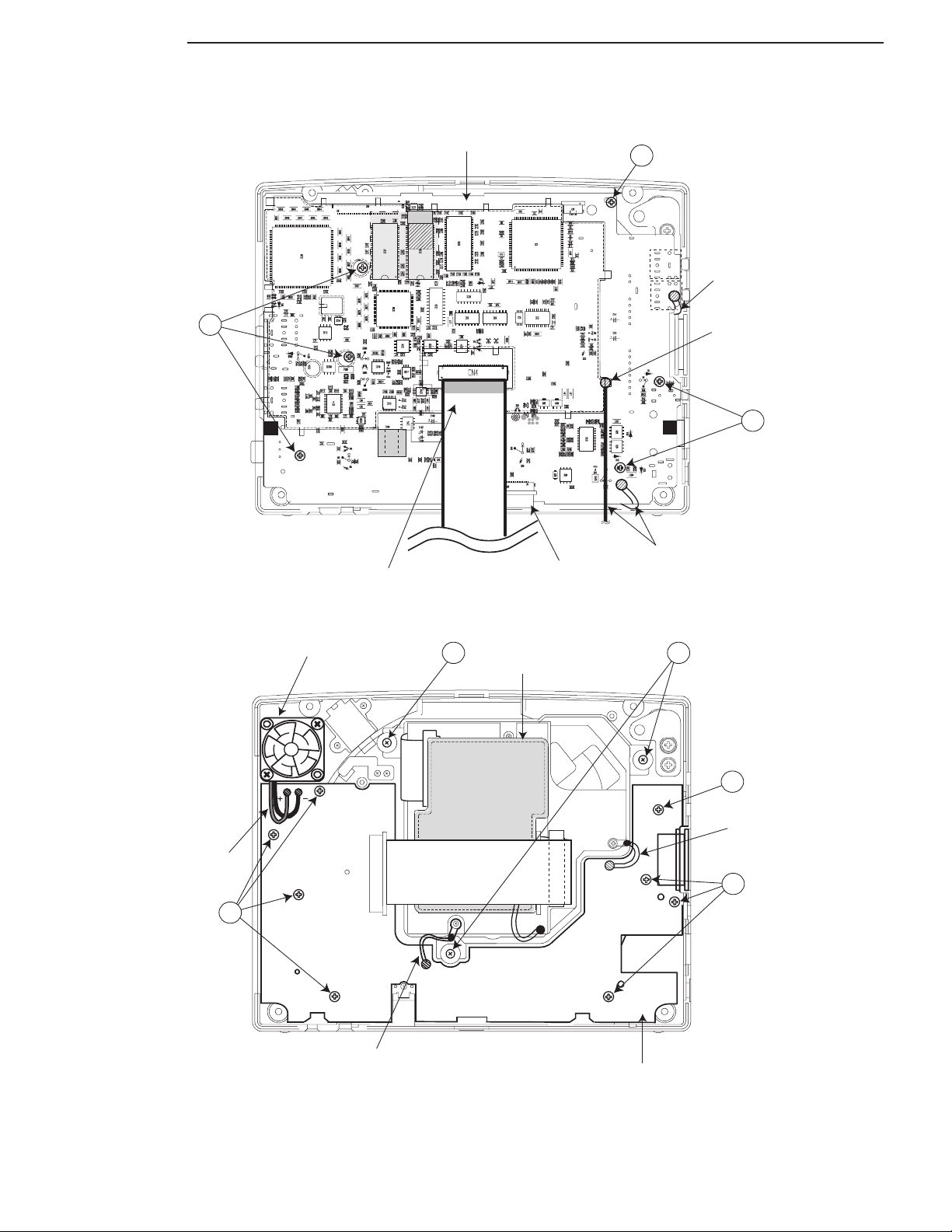
How to remove the PCB-ML,MAIN,DVD MECHANISM,MDVC07 and PCB-ML,DVD.
[Refer to figure 1,2,3]
1. Remove 4 screws A which fasten the REAR CABINET ASSY on the reverse side,
and the hook.
2. Remove FFC,50P which is connected to the PCB-ML,LCD and the PCB-ML,MAIN.
3. Remove the solder of LEAD WIRE which is connected to the PCB-ML,LCD and the PCB-ML,MAIN.
4. Remove 6 screws B which fasten the PCB-ML,MAIN.
5. Remove the solder of 2 LEAD WIRES which is connected to the PCB-ML,DVD.
6. Remove FFC,50P and FFC,34P which are connected to the PCB-ML,MAIN and the PCB-ML,DVD.
PCB-ML,MAIN can be removed.
7. Remove 3 special screws C which fasten the DVD MECHANISM,MDVC07.
8. Remove FFC,50P and the solder of 2 LEAD WIRES which is connected to the DVD MECHANISM,
MDVC07 and PCB-ML,DVD.
DVD MECHANISM can be removed.
9. Remove 8 screws D which fasten the PCB-ML,DVD.
10. Remove the solder of 2 LEAD WIRES placed on the FAN,MOTOR,DC side.
PCB-ML,DVD can be removed.
How to remove the PCB-ML,LCD. [Refer to figure 4]
4. Remove the 8 screws E which fasten the BRACKET,LCD and BRACKET-E,LCD.
5. Remove the solder of LEAD WIRE which is connected to the LCD.
1. Remove the FFC,14P from the PCB-W,KEY.
2. Remove the FFC,8P
3. Remove the FPC,32P from the LCD.
6. Remove the SOCKET from the DISPLAY MODULE.
from the touch screen.
PCB-ML,LCD can be removed.
How to remove the PCB-W,KEY. [Refer to figure 5]
1. Remove the solder of 4 LEAD WIRES which connected to from 2 speakers.
2. Remove the solder of 6 LEAD WIRES which connected to from PCB-W,DIMMER and PCB-W,DIMMER1.
3. Remove 3 screws F which fasten the PCB-W,KEY.
PCB-W,KEY can be removed.
How to remove the PCB-W,DIMMER and PCB-W,DIMMER1. [Refer to figure 5]
1. Remove 2 screws G and H which fasten the PCB-W,DIMMER and PCB-W,DIMMER1.
2. Remove the solder of 6 LEAD WIRES which connected to from PCB-W,KEY.
PCB-W,DIMMER and PCB-W,DIMMER1 can be removed.
HOOK
REAR CABINET ASSY Figure1
AA

_ _
9
LEAD,WIRE
FFC,50P
FFC,50P
LEAD,WIRE
SOLDER
FFC,34P
LEAD,WIRE
LEAD,WIRE
Figure2
Figure3
PCB-ML,MAIN
PCB-ML,DVD
DVD MECHANISM,
MDVC07
2 LEAD WIRES
PLACED ON FAN,
MOTOR,DC SIDE
FAN,MOTOR,DC
B
B
D
D
CC
D
B
DISASSEMBLY

_ _
10
E
E
Figure5
PCB-ML,LCD
PCB-W,KEY
OR
R
SHEET SHEET
BK
RBR YGN BKBL
PCB-W,DIMMERPCB-W,DIMMER 1
SPEAKER SPEAKER
SOLDER
SOLDER
BRACKET-E,LCD BRACKET,LCD
BRACKET,LCD
FFC,8P FFC,14P
FPC,32P
SOCKET BRACKET-E,LCD
Figure4
FG
G
H
H
E E
DISASSEMBLY

_ _
11
ADJUSTMENT PROCEDURES
Power supply voltage DC +9.0V.
Input the suitable signal for each adjustment at the time of the adjustment.
It shifts to TEST MODE by pressing in order of [OUT][OUT][IN][IN][VOLUME-][VOLUME+]
[VOLUME-][VOLUME+][RETURN][POSITION].
When in TEST MODE,the items can be changed by pressing [ ] or [ ] of joystick,
and the values can be changed by pressing [VOLUME+] or [VOLUME-].
Adjust each image adjustment value by the initial value at all the adjustment.
(COLOR/TINT/BLACK:CENTER,DIMMER:MAX,AUTO DIMMER:OFF)
<Adjustment conditions>
Insert the connector of the jig for the wave form observation into CN1007.
In VIDEO MODE,input monochrome 10 step signal from VIDEO IN.
Go to TEST MODE and adjust in order of the following.
Refer to a figure 1 for each measurement point.
COM Adjustment
Adjust "COM AMP" to become +5.5V±0.1Vp-p.
VB-B Adjustment
Adjust "RGB AMP" to become +4.5V±0.1Vp-p.
CONTRAST Adjustment
Adjust "CONTRAST" to become +3.2V±0.1Vp-p.
GAMMA Adjustment
Adjust "GAMMA 0" to make the fifth from black become +2.0V±0.1V(DC).
Adjust "GAMMA 2" to make the first from white become +3.5V±0.1V(DC).
Be careful that the first from white and the second from white do not approach too much.
(Give the difference in more than 0.2V.)
R/B Adjustment
Respectively adjust "SUB R" "SUB B" to make the fifth from black become +2.0V±0.1V(DC).
<Adjustment conditions>
Insert the connector of the jig for the wave form observation into CN1007.
IN NAVI MODE,display the present location.
Go to TEST MODE and adjust in order of the following
because NAVI screen become monochrome 10 step signal.
GAMMA Adjustment
Adjust "GAMMA 0" to make the fifth from black become +2.0V±0.1V(DC).
Adjust "GAMMA 2" to make the first from white become +3.5V±0.1V(DC).
The steps should be like figure 1 as the above - mentioned adjustment.

_ _
12
THE FIRST FROM WHITE BLACK LEVEL
SAME STEPS
VBB
WHITE LEVEL
THE FIFTH FROM BLACK
VBW
VBW BLACK-WHITE VOLTAGE
VBB BLACK-BLACK VOLTAGE
FIGURE 1
<Adjustment conditions>
Adjustment shall be done with the combination of a paired LCD module.
Display a map screen in the NAVI MODE.
Be within TEST MODE,and adjust it.
FLICKER ad
j
ustment
Adjustment bar is made "FLICKER".
Give a shock to the set,and adjust the value of "FLICKER" to make the FLICKER
visually optimal.
<Adjustment conditions>
Display the following level position adjustment screen in TEST MODE.
Adjust SVR1001 of the PCB-ML,LCD so that both ends of the screen
may become equally.
Make the white lines of both ends
become equality.
ADJUSTMENT PROCEDURES

_ _
13
<Adjustment conditions>
Insert the connector of the jig for the FREE RUN adjustment into CN1007.
Connect 6pin(CSYNC) of CN1007 to GND.
Select VIDEO or DVD MODE.(Any input is possible.)
Observe 7pin of CN1007 in the frequency counter.
FREE RUN Adjustment
Adjust SVR1003 to make the frequency of 7pin of CN1007 become 15.73kHz±0.01kHz.
<Adjustment conditions>
Go to TEST MODE.
Any mode can be adjusted.
TOUCH SCREEN Adjustment
Press the "touch" button on the bottom right of the screen,and display
the TOUCH SCREEN adjustment screen.
adjust TOUCH SCREEN adjustment jig in accordance with
the indication of the screen.
ADJUSTMENT PROCEDURES

_ _
14
EXPLANATION OF MICROCOMPUTER
IC 1151 (HD64F3039TEBL18)
Pin
1
2
3
4
5
6
7
8
9
10
11
12
21
29
30
31
32
33
34
35
36
37
38
39
40
41
42
43
44
45
46
47
48
49
50
51
52
53
54
55
56
57
58
59
60
65
66
67
68
69
70
71
72
73
74
75
76
77
78
79
80
+5V
NC
READ
System clock output
CPU hard ware standby terminal +5V
CPU hard reset +5V
GND
Crystal connection terminal
CPU address bus
0V
NC
RF AMP prescaler
+5V
GND
I
-
I
I
O
I
I
-
-
I
NC
Chip select output
Chip select output
NC
NC
Inside switch input
NC
Cover OPEN / CLOSE SW input
IDE cable select input
NAVI ,DVD change terminal(Low at NAVI)
NC
GND
NC
-
-
I
-
O
O
I/FEW
VCC
RXD
NC
ENCODER
/ATAINT
/SDINT
TXD
TEST CNT
NC
AVCC
AVSS
FE
LVL
NC
/RD
/WR
VSS
EXTAL
RES
NMI
NC
PSC
MD0
CSEL
XTAL
-
I
I
I
-
MD1
PHI
STBY I
O
-
-
O
I
I
-
O
O
-
NC
SRVDPCS
ATACS
-
-
-
I
-
I
NC
CLOSESW
NAVI
NC
NC
LOEJKEY
INSIDE
VSS -
+5V
-
GND
VCC -
PLL output
Flash memory output
AUDIO Disc play : H
H : Standby, L : Operation mode
AUDIO
/G
VSS
O
H : MUTE ON / L : MUTE OFF Rch
Normally 5V,boot flash writing 0V
Spindle motor driver power save
H : Operation mode, L : Standby
H : MUTE ON / L : MUTE OFF Lch
O
O
-
MD2
LSPEED
FLCNT
I
O
O
O
O
O
SPDRVPS
G
MUTEL
MUTER
/RST0 O ATAPI controller/decoder reset
/RST1 O Servo/data processor reset
Signal I/O Function
Servo/decoder processor interrupt input
Serial data trans terminal for debug
Serial data receive terminal for debug
Test mode input
NC
+5V
22
28
HA0
HA6
O
ATAPI controller/decoder interrupt input
SUM signal input
WRITE
Flash memory output
GND
Focus error signal input
HA7
13
20
D0
D7
I/0 CPU data bus
DIR
DVDR
NC
ENCODER pulse input
Analog +5V power down control output/PWR DWN1 O
RFMVON
NC
O
O
O
O
O
-
/PWR DWN2
STBY
Laser RF output DVD : H
NC
61
64
TEST0
TEST4
I KEY input terminal for TEST
Digital +5V power down control output
PWN driver MUTE output STBY : L
H : DSP output, L : DSP input
DVD-R disc : L OTHER disc : H

_ _
15
EXPLANATION OF MICROCOMPUTER
IC 1 (M30802) 1/2
Pin
1
2
3
4
5
6
7
8
9
10
11
12
13
14
15
16
17
18
19
20
21
22
23
24
25
26
27
28
29
30
31
32
33
34
35
36
37
38
39
40
41
42
43
44
45
46
47
48
49
50
51
52
53
54
55
56
57
58
59
60
61
62
63
64
65
66
67
68
69
70
71
72
73
74
POWER on/off output
GND
AMP ON/OFF output
Power supply 4.2V-5.5V
TV MODE output
VIDEO MODE output
NAVI MODE output
DVD MODE output
GND
GND
FRASH writing
TOUCH SCREEN control
GND
Parking judgement input
AUDIO CD judgement input
DVD RESET signal
FRASH writing
Vertical synchronizing signal input
GND
Remote controller input
GND
AUDIO change switch
AUDIO change switch
RESET input
NC
NC
NC
NC
Function
MAIN-DVD communication
Clock input for the DVD
Dimmer output
AMP2
/NV_RST
S
ignal
MAIN_DVD
DVD_CLK
DIMOUT
NAVI
DVD
BOOT4
RAS
AMP ON/OFF output
NAVI recovery
BOOT3
-
POWER
VSS
FRASH writing
NC
AMP1
VCC
MAIN-ASIC
ASIC-MAIN
FRASH writing
GND
TP_Y
TP_X
TV
VIDEO
TOUCH SCREEN control
SH communication
SH communication
KEY_TX
VCC
REVERSED
VSS
RS232C output
Power supply 4.2V-5.5V
BOOT2
TPCONT
CDCHK
DVD_RST
SCL
SDA
VD_IN
BEEP
I2C BUS communication
DVD_INT
FMT_CE
FMT_MUTE
PARK_I
INT output for the DVD
GND
VIDEO input
BEEP output
XIN
VCC
BOOT1
VSYNC
MAIN clock oscillator input
Power supply 4.2V-5.5V
DARC_INT
RMC
AU_SW2
/RESET
XOUT
VSS
TU_LE
TU_LOCK
MAIN clock oscillator output
GND
TU_SD
BYTE
CNVSS
AU_SW1
NC
Hi input
NC
NC
DARC_MAIN
DARC_CLK
DARC_CE
DARC_RST
NC
NC
TU_CLK
TU_DATA
VOL_0
MAIN_DARC
DAC output for the volume adjustment
NC
O
O
I
I
-
O
O
O
I
O
O
O
O
O
I
O
O
I
O
I
I
O
I/O
I/O
O
O
O
I
I
I
I
O
I
I
I
O
I
O
I
I
I
O
O
O
O
I
I
O
O
O
I
O
O
O
P132
Vcc
P131
P130
P55
-
P133
Vss
P135
P134
P57
RAS
P61
P60
P137
P136
P65
P64
TXD0
RXD0
TXD1
Vcc
RXD1
Vss
P73
P72
SCL2
SDA2
P77
P76
P75
P74
INT1
INT0
P81
P80
Xin
Vcc
NMI
INT2
P86
RESET
Xout
Vss
P140
BYTE
CNVss
P87
P144
P143
P142
P141
RXD3
CLK3
P146
P145
CLK4
DA1
DA0
TXD3
Port
TXD4
I/
O
O
-
RD
-
WE
P127
P126
P125
-
O
-
O
O
O
O
-
WE
-
CAS
LMUTE
VOL_CLK
VOL_DATA
NC
GND
NC
Pull-up
LINE OUT MUTE output
GND
GND
-
-
-
-
VMUTE
VCC
-
-
-
-
A19
Vcc
OVMUTE output
Power supply 4.2V-5.5V
-
-
NC
NC
NC
NC
-
-

_ _
16
IC 1 (M30802) 2/2
Pin
75
76
77
78
79
80
81
82
83
84
85
86
87
88
89
90
91
92
93
94
95
96
97
98
99
100
101
102
103
104
105
106
107
108
109
110
111
112
113
114
115
116
117
118
119
120
121
122
123
124
125
126
127
128
129
130
131
132
133
134
135
136
137
138
139
140
141
142
143
144
S
ignal Function
A18
Vss
Port I/
O
A17
A16
A15
A14
A13
A12
A11
A10
A9
P124
P123
P122
P121
P120
Vcc
-
-
-
Vss
-
-
-
P14
P13
O
-
P17
P16
P15
-
-
O
O
O
O
O
O
O
O
O
O
O
I
O
O
-
-
-
-
-
-
O
I
RESERVED
VSS
-
O
O
O
-
-
RESERVED
RESERVED
RESERVED
RESERVED
RESERVED
RESERVED
RESERVED
RESERVED
RESERVED
-
FMLVL
DOOR
SMUTE
DMUTE
VCC
-
-
-
VSS
-
-
-
KS3
K0
NC
GND
-
KS0
KS1
KS2
-
-
NC
NC
NC
NC
NC
NC
NC
NC
NC
NC
GND
DOOR detect
Audio mute output
Image mute output
Power supply 4.2V-5.5V
NC
GND
NC
NC
NC
NC
NC
NC
NC
NC
GND
GND
GND
GND
Key return
P12
P11
I
I
K1
K2
Key return
Key return
P10
D7
D6
D5
D4
-
-
P112
P111
P110
D3
D2
D1
D0
P157
P156
P155
P154
P153
P152
P151
Vss
P150
Vcc
AN7
AN6
AN5
AN4
AN3
AN2
AN1
Avss
AN0
Vref
Avcc
RXD4
I
I/O
I/O
I/O
I/O
-
-
I
I
I
I/O
I/O
I/O
I/O
O
O
O
O
O
O
I
O
I
I
I
I
I
I
I
-
I
K3
RESERVED
RESERVED
RESERVED
RESERVED
-
-
PARK_SW
M_ID1
TEST
RESERVED
RESERVED
RESERVED
RESERVED
LCD_CLK
LCD_DATA
LCD_CS
DM2
DM3
OSD_SW
M_ID2
VSS
LIGHT
VCC
X_AD
Y_AD
DCCHK
TEMP
BAT_I
DIMIN
SMETER
AVSS
SYS_REV
VREF
AVCC
DVD-MAIN
GND
NC
NC
NC
NC
NC
NC
Parking cable plug input
GND
TEST MODE judgement input
NC
NC
NC
NC
LCD I/F CLOCK
LCD I/F DATA
LCD I/F TIP SELECT
LCD MODE output
LCD MODE output
OSD expression output
GND
GND
BACKLIGHT control
Power supply 4.2V-5.5V
TOUCH SCREEN input
TOUCH SCREEN input
Input of power supply confirmation
Input of temperature detection
Input of voltage detection
Dimmer sensor input
GND
Analog GND
Revision distinction
A-D reference voltage
Analog power supply
DVD-MAIN communication
EXPLANATION OF MICROCOMPUTER

_ _
17
EXPLANATION OF MICROCOMPUTER
IC 20 (HD6417706) 1/3
Pin
1
2
3
4
11
12
13
19
20
21
22
23
24
25
26
27
37
38
39
49
50
51
61
62
63
71
72
73
74
75
76
77
78
79
80
81
82
83
84
85
86
87
88
89
90
Signal I/O Function
LLVcc POWER +1.9V
XTAL2
EXTAL2
GND
GND
SD25
LVcc
LLVcc
SD18
SD17
GND
SD16
GND
SD15
LVcc
GND
LVcc
GND
SA4
LVcc
RD/WR
/WE3
SA24
SA25
GND
SA22
LVcc
GND
SA14
O
I
NC
Pull-up
I/O
/CS2
/CS3
/CS4
/CS5 O
POWER
I/O
I/O
POWER
I/O
POWER
POWER
GND
/CS0
LVcc
/WE0
/WE1
/WE2
I/O
I/O
/BS
/RD
SA23
LVcc
I/O
POWER
I/O
POWER
I/O
I/O
I/O
O
O
O
O
O
O
+1.9V
Data bus
Data bus
Data bus
GND
Data bus
GND
52
60
64
70
Address bus
Address bus
+3.3V
Address bus
+3.3V
GND
Address bus
45
48
Read/write select signal
SA0
SA3
OAddress bus
SA5
SA13
I/O
SA15
SA21
I/O
D15-D8 select signal
28
36
SD14
SD6
I/O
40
44
SD4
SD0
I/O
I/O
POWER
SD5
GND
Data busI/OSD19
GND
Data bus
+3.3V
Data bus
14
18
SD24
SD20
I/O
+3.3V
Data bus
Chip select 3
Chip select 4
Address bus
+3.3V
Address bus
Chip select 5
D23-D16 select signal
D31-D24 select signal
POWER
GND
Address bus
O
O
O
O
O
Address bus
NC
Read strobe
D7-D0 select signal
GND
GND
Data bus
+3.3V
5
10
SD31
SD26
I/O Data bus
Data bus
GND
Chip select
+3.3v
NC

_ _
18
EXPLANATION OF MICROCOMPUTER
IC 20 (HD6417706) 2/3
Pin
91
92
93
94
95
96
97
98
99
100
101
102
103
104
105
106
107
108
109
110
111
112
113
114
115
116
117
118
119
120
121
122
123
124
125
126
127
128
129
130
131
132
133
134
135
136
137
138
139
140
141
142
143
144
145
146
147
148
149
150
Pull-up
+1.9V
SCI receive data0
SCI receive data2
External interrupt request(MAIN)
GND
NC
Pull-up
SC port
NC
GND
System clock input/output(39.3216MHz)
+3.3V
SCI transmit data0
Processor status
Processor status
Pull-up
ADPCM SW
External Clock/crystal oscillator pin
Pull-up
GND
Colck oscillator pin
PLL2 external capacitance pin
+1.9V
+1.9V
PLL1 external capacitance pin
GND
GND
NC
Pull-up
Pull-up
Pull-up
NC
LLVcc POWER
GND
/RESETM
I
I
IRQ5
SCPT[4]
RxD0
RxD2
I/O
I
I
SCPT[3]
POWER
O
I/O
O
O
LVcc
TxD0
SCK0
TxD2
CKIO O
GND
STATUS0
STATUS1
O
PTE[6]
PTE[7]
I/O
I
I
O
O
EXTAL
-
-
POWER
I
LLVcc
MD1
GND
XTAL
CAP1
GND
GND
CAP2
LLVcc POWER
Input/output port F
Pull-up
GND
Pull-up
+3.3V
PTF[5]
PTF[6]
/ASEMD0
I/O
I/O
I
NC
Input/output port F
Pull-up
LLVcc
PTG[2]
PTG[3]
I
POWER
I
I
Input/output port E
Input/output port F
PTG[0]
GND
PTG[1]
I
I
I
O
I
PTF[1]
PTF[2]
PTF[3]
PTF[4]
PTE[2]
PTE[3]
PTF[0]
I
I
I
DMA acknowledge 0
DMA acknowledge 1
Input/output port E
Pull-up
NC
Pull-up
Hardware wait request
/DACK0
/DACK1
O
O
/BACK
/BREQ
/WAIT
O
I
I
/IOIS16
I/O
I
Input/output port D
+3.3V
Lower32 Mbytes address RAS
Input/output port D
Lower32 Mbytes address CAS
NC
NC
PTD[3]
PTD[4]
O
POWER
O
O
O
I/O
PTD[7]
LVcc
/CAS
/RAS
PTD[1]
/CE2A
GND
ONC
GND
/CS6 O Chip select 6
Signal I/O Function

_ _
19
EXPLANATION OF MICROCOMPUTER
IC 20 (HD6417706) 3/3
Pin
151
152
153
154
155
156
157
158
159
160
161
162
163
164
165
166
167
168
169
170
171
172
173
174
175
176
I
DMA request
Input port G
Pull-down
Pull-down
Power-on reset request
Pull-up
I
I
I
I
I
I
I
I
I
I
I
I
I
I
POWER
I
I
I
I
I
PTJ[2]
PTJ[3]
LVcc
GND
MD5
GND
PTJ[0]
PTJ[1]
/RESETP
CA
MD3
MD4
/DREQ1
PTG[5]
MD0
MD2
NMI
LVcc
PTG[4]
/DREQ0
IRQ2
IRQ3
IRQ4
GND
Signal I/O Function
IRQ0 I External interrupt request(Q2)
IRQ1
DMA request
GND
Pull-up
+3.3V
Pull-up
External interrupt request(ATAPI)
External interrupt request(FM)
External interrupt request(BEACON)
External interrupt request(GYRO)
Pull-down
Pull-up
Pull-down
GND
GND
GND
GND
GND
+3.3V
GND
POWER
Other manuals for NV-E7500 - Navigation System With DVD Player
1
Table of contents
Other Sanyo Car Video System manuals
Popular Car Video System manuals by other brands

Boss Audio Systems
Boss Audio Systems BV-560M owner's manual

Blaupunkt
Blaupunkt 900 Series operating instructions

Pioneer
Pioneer AVH-P6600DVD Operation manual

Kenwood
Kenwood LZH-100W - DVD Player With LCD Monitor instruction manual

Intec
Intec car vision CVD650LCD user guide

Mopar
Mopar 82208655AB installation instructions