No. 5995-5/34
LC78626KE
Continued from preceding page.
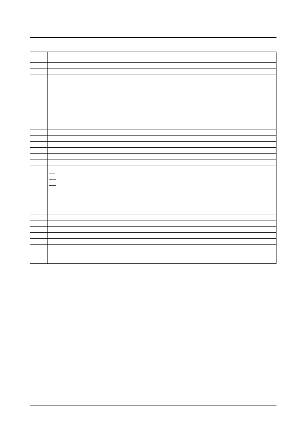
Parameter Symbol Conditions Ratings Unit
min typ max
DEFI, EFMI, HFL, TES, RWC, COIN, CQCK,
FMT, MR1, MR2, RES, TESD, WOK,
Input low-level current IIL PAUSE IN, SHOCK, TESCLK, TESA, TESB, –5 µA
TESC, TESGB, TAI, TEST1 to TEST5, CS :
VIN = 0 V
EFMO, CLV+, CLV–, V/P, TOFF, TGL, JP+,
VOH1 JP–, PCK, FSEQ, EFLG, FSX, EMPH : 2.56 V
IOH = –1 mA
CONT2 to CONT5, SBSY, MUTEL, MUTER,
Output high-level current VOH2 C2F, WRQ, SQOUT, 16M/NGJ, 4.2M, EMPP, 2.56 V
OVF, CNTOK, NGJ : IOH = –0.5 mA
VOH3 DOUT : IOH = –12 mA 2.72 V
VOH4
OE, WE, CAS, RAS, AD10/CAS2, AD9 to AD0,
2.56 V
DRAM3 to DRAM0 : IOH = –0.5 mA
VOH5 MMC0 to MMC3 : IOH = –2 mA 2.24 V
VOL1EFMO, CLV+, CLV–, V/P, TOFF, JP+, JP–, 0.64 V
PCK, FSEQ, EFLG, FSX, EMPH : IOL = 1 mA
CONT2 to CONT5, SBSY, MUTEL, MUTER,
VOL2 C2F, WRQ, SQOUT, 16M/NGJ, 4.2M, EMPP, 0.32 V
Output low-level current OVF, CNTOK : IOL = 2 mA
VOL3 DOUT : IOL = 12 mA 0.48 V
VOL4
OE, WE, CAS, RAS, AD10/CAS2, AD9 to AD0,
0.44 V
DRAM3 to DRAM0 : IOL = 0.5 mA
VOL5 MMC0 to MMC3 : IOL = 2 mA 0.96 V
PDO, CLV+, CLV–, JP+, JP–,
IOFF1 CONT2 to CONT5, DRAM0 to DRAM3, 5 µA
Output off leakage current ASRES : VOUT = VDD
PDO, CLV+, CLV–, JP+, JP–,
IOFF2 CONT2 to CONT5, DRAM0 to DRAM3, –5 µA
ASRES : VOUT = 0 V
Charge pump output current IPDOH PDO : RISET = 68 kΩ30 42 54 µA
IPDOL PDO : RISET = 68 kΩ–54 –42 –30 µA
Parameter Symbol Conditions Ratings Unit
min typ max
Total harmonic distortion rate TRD+N LCHO, RCHO; 1 kHz: Uses the 0 dB data 0.035 0.038 %
input and the 20 kHz-LPF (in the AD725D)
LCHO, RCHO; 1 kHz: Uses the –60 dB data
Dynamic range DR input, the 20 kHz-LPF (in the AD725D), and 81 84 dB
the A filter
LCHO, RCHO; 1 kHz: Uses the 0 dB data
Signal to noise ratio S/N input, the 20 kHz-LPF (in the AD725D), and 87 92 dB
the A filter
Cross talk CT LCHO, RCHO; 1 kHz: Uses the 0 dB data 79 82 dB
input and the 20 kHz-LPF (in the AD725D)
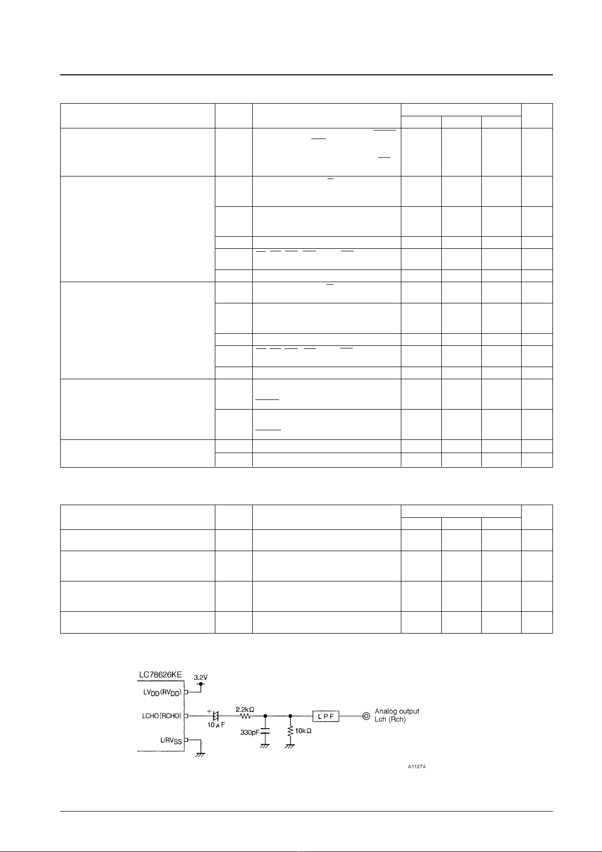
One-bit D/A Converter Analog Characteristics at
Ta = 25°C, VDD = LVDD = RVDD = 3.2 V, VSS = L/RVSS = 0 V
Note: Measured with the normal-speed playback mode in the Sanyo one-bit D/A converter block reference digital attenuator circuit.