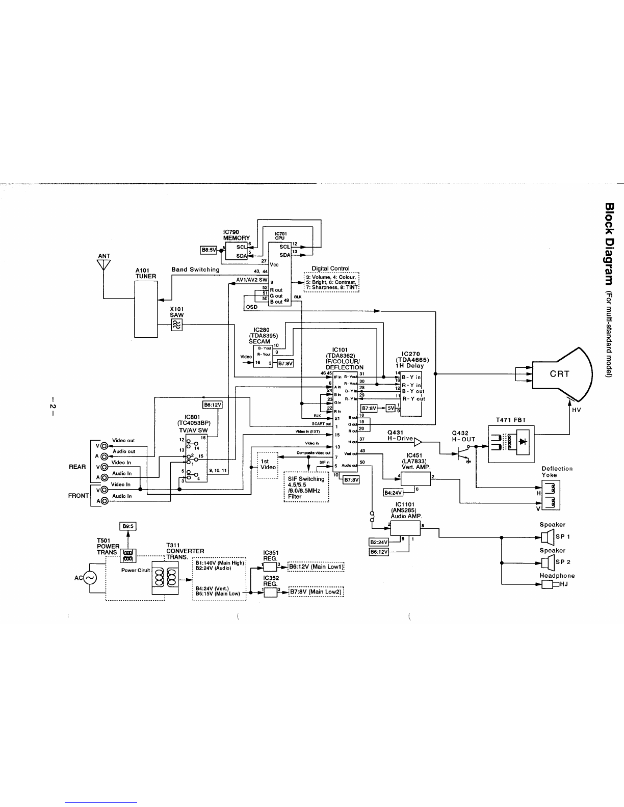
Sanyo CP25SE1 User manual

FILE NO.
SERVICE MANUAL Colour Television Model No. CP25SEI
(Australia/New Zealand)
Service Ref. No. CP25SEI -00
Specifications
Power Source .................... AC 220 – 240 Volts, 50 Hz.
Colour System ................... pAL-WG Product Code: 111335518
and Television Svstem (AV input: PAL/NTSC/NTSC4.43/PAL- 60Nz)
Channel Coverage .............VHF: 0-11, 5A (Australia), 1-11 (New Zealand)
LOriginal Version
UHF: 28- 69(Australia), 21- 69(New Zealand)
CATV: S1 -S41 ,X, Y, “Z, Z+l ,Z+2
Video IF.,., ......................... 38.9MHz
Aerial Input Impedance ...... 75 Q
Ext. Terminals ....................
>’ AV inputs:
Video inputs: Phono jack x1
Audio inputs: Phono jack x1
AV outputs:
;Video outputs: Phono jack x1
Audio outputs: Phono jack x1
Headphone Jack: Mini, Jack x1
Sound Output (Music) ........ 5.0 W
Dimensions ........................ 588(W)X531 (H)x455(D)mm
Weight(approx.) ................. 29 Kg
Specifications subject to change without notice.
Chassis Series: AAl -A
Give complete “SERVICE REF. No.” for parts
order or servicing. It is shown on the rating plate
at the cabinet back of the unit.
This T.V. receiver will not work properly in
foreign countries where the television trans -
mission system and power source differ from the
design specifications. Refer to the specification
table.
LF6EY REFERENCE NO. SM 51025

I
Iv
I
REAR
FRONT
ANT
A101
TUNEF
IC790
=-TE-!w
Xlol
SAW
5’
B6:12V
IC801
(TC4053BP)
k
Digital Control
.......................-.7
~3: Volume, 4: Colour, ;
5: Bright, 6: Contrast, :
\7: Sharpness, 8: TINT:
..........................4
Es-K
10SD —
d
IC280
(TDA8395)
SECAM
B-YCUI‘:
~dso R-‘fUA
16 3B7:8V
Iclol
(TDA8362)
lF/COLOUR/
_-
@
...................:
IC270
(TDA4665)
1HDelay
DEFLECTION
4645 31 14
bIF hB-VU< (
~B-Y in
6R-Yml .30 ~R-Y in
%‘h B.Y~ :6
+Bh B-Y out
29
23 R-Yh -“R-Y oh
1*oh
22
+Rim
UK +21 BM 116
SCARTal 19
N/AV SW 1‘m Z.
Vti In (Em Rwl
16 E15 Q431 Q432
—12 ~37 H- Drive~ H-OUT
Vmea1“ Hu$.
,3 074 -13
—~43
A@ 2 15 .......... Cmlwe Vidw cd Vti d,
—
Ir
7IC451
Video In SIF h50 (LA7633)
v@ 5A&b out—Vert. AMP,
.............. ....1
:10
SIF Switching :42
—
rVideo In A4.5/5.5
VQ ~i:~.5MHz !~3
Audio In H
A@ Icllol “3
(AN5265) v
Audio AMP.
T501
POWER
TRANS
------ ‘-””----”-””: TRANS. r-----------------------;
Acq ~.N$~~::&:z:
CRT
HV
Deflection
Yoke
8Speaker
IB2:24V Jg ‘
ISP 1
B6:12V Speaker
?SP 2
............................ ..........................
( (

Block Diagram (Forrnul~-standardmodel)
...........................................”
&AS1
(D106)
NTSC
Band Limited
--J
101[TDA8362
Vin
:in
TvOut
SECAM
REF
IF in
CHROMA ID
TV ID
(TIME BASE
34 35
I
I
------
6.5 MHz Filter ~%
S11
(QI56)
,....,
6.oMHz Filter j’+%
Slo
-..
(Ql 55)
-----
5.5 MHz Filter
—+% S9
(Q154)
,....,
4.5 MHz Filter l+k
SIF Filter S6
(Q153)
I
~----------: s~ 5.5 MHz Trep
I r=~’20)J 4.5MHz Trap I
Sound Cam.er Trap +
[L+- ‘IJ
D121) 5.5/6 .O/6.5MHZ TreP
+--- :
INV IC260
*
(Q157) SECAM
1REF.
19,
S4 ......
............
................................................
IC701 (CPU) !
SECAM~$1.j
18
+CID.
4TV ID.
42 4.43MHZ
.....
--43 3.58MHZ
V-SYNC.
2V-SYNC. Pulse
(for O.S.D.)
...................................
........................................
:!
::
::
..............................................
...................................................
-3–

Circuit Description
1. POWER SUPPLY
The power supply circuit of the AAl -Achassis is
composed of arectifier smoothing circuit, an oscillation
circuit, acontrol circuit and an output rectifier circuit.
The AC input voltage is full-wave rectified by the rectifier
smoothing circuit, and an unstable DC voltage is
generated at both terminals of the smoothing capacitor
C307. This voltage is input to the oscillation circuit. The
oscillation circuit is provided with ablocking oscillator
circuit that switches the switching transistor Q313 ON and
OFF, and an oscillation frequency and aduty square
wave pulse are generated in the input windings according
to operation of the control circuit. Asquare- wave pulse
whose size is dependent on the turn ratio of the input and
output windings is obtained in the output winding. This is
rectified in the output rectifier circuit, and the desired DC
voltage is obtained.
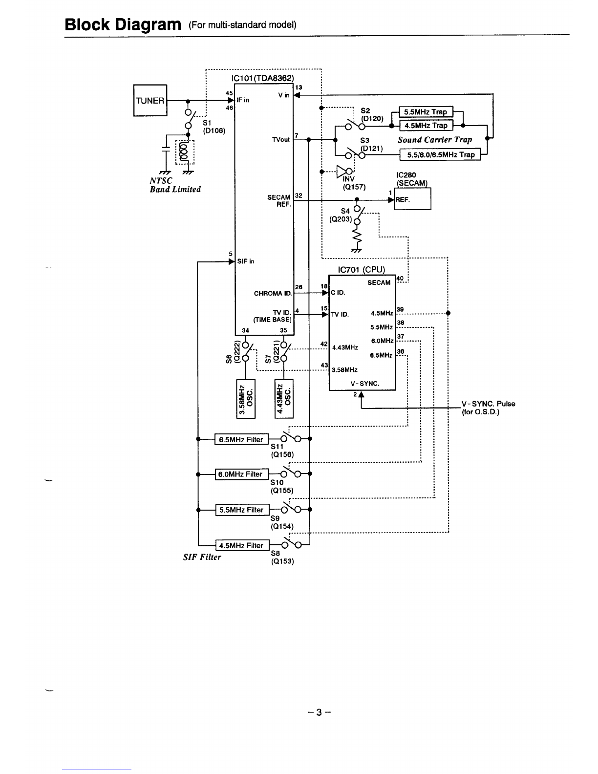
2. IF& DEFLECTION
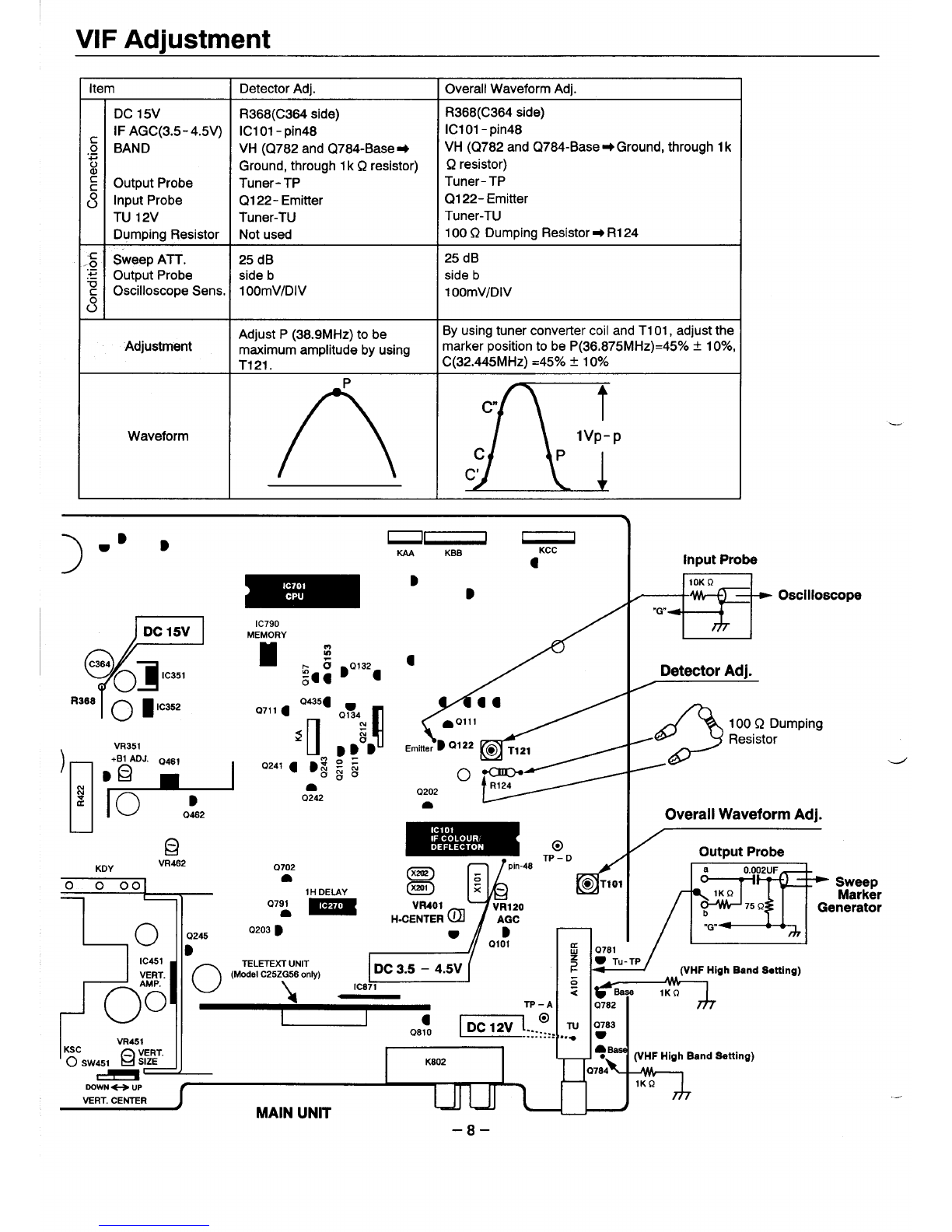
The IF output signal from the tuner passes through the
SAW filter, and it is input to pin45 and pin46 of ICI 01.
The signal input to the IC passes through the IF amplifier,
video detection and video amplifier circuits and is output
from pin7 as a composite video signal.
And after this signal is converted to impedance at Q134,
supplies to the video and chroma amplifier stages.
The output signal from pin7 passes through the
5.5MHz(B/G)/6.0MHz( l)/6.5MHz(D/K)/4 .5MHz(M) filtering
circuit, and it is input to pin5 of IC101. The signal input to
the IC passes through the SIF amplifier, FM detector,
external audio switch and audio output circuit, and it is
then output from pin50 as audio drive signal.
The sync. -separation circuit separates the video signals
applied to pinl 3or pinl 5to vertical- and horizontal- sync.
signals respectively.
The horizontal oscillator requires no external components
and is fully integrated. The oscillator is always running
when the start- pin36 is supplied with 8V.
Horizontal drive signal is output from pin37. VR401 is for
adjustment of the horizontal centering.
The separated vertical sync. signal from sync. separation
circuit passes through the vertical -separation circuit, and
applied to trigger divider circuit.
The horizontal oscillation pulse and input vertical sync.
pulse are monitored by the trigger divider circuit, and
switching 50Hz and 60Hz system, the vertical amplitude
automatically adjusted for 50Hz and 60 Hz.
The output signal from the trigger divider is triggered
vertical oscillation circuit consisting of R401 ,C402 and
pin42, and vertical drive pulse is output from pin43.
VR451 is for changing the amount of AC feedback applied
to pin41 and for adjustment of the vertical amplitude.
3. VIDEO CHROMA
The composite video signal output from the pin7 of [Cl 01
passes through Q122/ Q134, and it is supplied to pin13.
The external video signal output from AV terminal passes
through IC801, and it is supplied to pin15.
The video signal input to pin13 or pin15 is separated to
luminance (Y) signal and chroma signal in IC101. These
pins are used in common with H/V -sync. separation
input.
The peaking of Ysignal is adjusted by DC voltage of
pin14.(’’SHARPNESS” control)
The chroma signal is divided into R-Y, B-Ychroma
signals, demodulated in IC101,
and output from pin30 (R -Y) and pin31 (B -Y). These
chroma signals pass through the 1Hdelay line circuit
(IC270), and they are input to pin29 (R- Y) and pin28 (B-
Y). These R-Y/B -Ysignals pass through RGB matrix
circuit and RGB selector circuit of IC101. The internal
RGB signals are generated in RGB matrix circuit and the -
RGB selector, consisting linear amplifiers, clamps and
selects either the internal RGB signals or the external
RGB signals input from pin22 (R) ,pin23 (G), pin24 (B).
Selection is controlled by the voltage at the RGB switch
control (pin21 )and mixed RGB modes are possible since
RGB switching is fast.
The RGB switch also functions as a fast blanking pin by
blanking the RGB output stages; here internal and
external RGB signals are overruled.
The colour gain is controlled by DC voltage of pin26.
(“COLOUR” control)
The contrast control voltage present at pin25, controls the
RGB signal gain, and the brightness control voltage
present at pin17 controls DC level of RGB signals.
The RGB signals are finally buffered before being
available at the RGB output pins [pin20 (R), pin19 (G),
pin18 (B)]. d
4. AUDIO OUTPUT
The audio signal output from pin50 of IC101 is input to
pin2 of IC1 101 and passes through the pre -amplifier
circuit and drive circuit, after which it is input to the audio
amplifier. The audio amplifier is an SEPP (Single- Ended
Push Pull) type and output to pin8 to directly drive the
speaker.
.-.’
–4–

Circuit Description
5. VERTICAL OUTPUT
.An IC (LA7833) is used for the vertical output circuit in this
chassis. The vertical drive pulse from pin43 of ICI 01 is
input to pin4 of IC451. This pulse drives IC451, and
vertical scanning is performed. In the first half of scanning
adeflecting current is output from pin2 and passes
through the following path:
VCC(B4) +D451 +pin3 +pin2 +DY +C461 +
vR451/R459.
An electric charge is then stored in C461. In the last half of
scanning the current path is:
C461 +DY +pin2+ pinl +VR451/R459+ C461
In this way, an amplifying sawtooth waveform current
flows directly to DY to perform electron beam deflection.
LNext, in the first half of the blanking period the vettical
drive pulse suddenly becomes OFF, and in order to
reduce the current flowing to DY, the current path
becomes as follows by the inductance of DY:
DY+ pin2 +pinl +VR451/R459 *C461 +DY
Also, when the charge of DY has dissipated, the current
path becomes:
Vcc+ pin6+pin7+C452+ pin3+ pin2+ DY+C461 +
VR451 /R459
and when the prescribed current value is reached, the
vertical drive pulse becomes ON. This completes one
cycle.
6. HORIZONTAL OUTPUT
Ahorizontal oscillation signal is output from pin37 of
bIC101 and switches the drive transistor Q431. This
switching signal is current amplified by the drive
transformer T431 and drives the output transistor Q432.
When Q432 becomes ON, an amplifying current flows
directly to DY through
C441 /C442 +L441 /R441 *DY +Q432- C+Q432- E
and deflection is performed in the last half of the scanning
period. Next, when Q432 becomes OFF, the charge that
had been stored in DY up to that point releases a
resonance current to the resonant capacitors C420 and
C423 and charges them. The current stored in C420 and
C423 is then flowed back to DY, and an opposite charge
is then stored in DY. This opposite charge then switches
the dumper diode in Q432 ON, the resonance state is
completed, and an amplifying current is then flowed again
b
directly to DY through the dumper diode.
By this means, deflection in the first half of the scanning
period is performed ,and when Q432 becomes ON at the
end of the first half of the scanning period, deflection
during the last half is begun, thus completing one cycle.
7.SYSTEM SWITCHING
(For multi- standard modei)
The system switches (S1 -S11 )are used for muiti -
standard model.
(Refer to Block Diagram of system switching circuit)
S1:Switch for band-limiting on NTSC(3.58) mode (D106)
This switch is driven by ON/OFF signal of CPU
(pin39).
S2:Switch for sound carrier trap on NTSC(3.58) mode
(D120)
This switch is driven by signai of CPU (pin39) too.
S3:Switch for sound carrier trap except NTSC(3.58) mode
(D121)
This switch is driven by invetting signal of CPU
(pin39).
S4:System switch for forced SECAM mode (Q203)
This switch is driven by ON/OFF signal of CPU
(pin40).
S6:System switch for forced 4.43 mode (Q222)
This switch is driven by ON/OFF signai of CPU
(pin41).
Note: When the colour system is set to “AUTO, both S6
and S7 will turn on.
S7:System switch for forced 3.58 mode (Q221 )
This switch is
(pin42).
S8:System switch
mode (Ql 53)
This switch is
(pin39).
S9:System switch
(Ql 54)
This switch is
(pin38).
driven by ON/OFF
for 4.5MHz fiitering
driven by ON/OFF
for 5.5MHz filtering
driven by ON/OFF
SIO:System switch for 6.OMHZ filtering on
This switch is driven by ON/OFF
(pin37).
signai of CPU
on NTSC(3.58)
signai of CPU
on B/G mode
signal of CPU
imode (Ql 55)
signal of CPU
S1l’:System switch for 6.5MHz filtering on D/K mode
(Q156)
This switch is driven by ON/OFF signal of CPU
(pin36).
Note: When the TV system is set to “AUTO, S8, S9, S1 O
and S11 will turn on.
–5–
Table of contents
Other Sanyo TV manuals

Sanyo
Sanyo C29LF39 User manual

Sanyo
Sanyo CE19LD08-B User manual

Sanyo
Sanyo CE28FWH2F-C User manual

Sanyo
Sanyo 14MT1 User manual

Sanyo
Sanyo DS27820 User manual

Sanyo
Sanyo CZP2515V User manual

Sanyo
Sanyo C21TF26S User manual

Sanyo
Sanyo C20LB98M User manual

Sanyo
Sanyo C25ZG45 User manual

Sanyo
Sanyo DS27431 User manual

Sanyo
Sanyo CP29SV2Z User manual

Sanyo
Sanyo C21PM86Z User manual

Sanyo
Sanyo CE24WN5-B User manual

Sanyo
Sanyo CP14SE1 User manual

Sanyo
Sanyo CP21SE1K(S) User manual

Sanyo
Sanyo CTP8680 User manual

Sanyo
Sanyo DS27820 User manual

Sanyo
Sanyo C21ES35 User manual

Sanyo
Sanyo AVM-27D6 User manual

Sanyo
Sanyo CP20SR1Z User manual