Sanyo CZP2940TXN User manual

SAjI/YO
SERVICE MANUAL
.
L
QSpecifications
Colour Television
IFILE NO. I
Model No. CZP2940TXN
(New Zealand)
Service Ref. No. CZP2940TXN -00
t
1
Power Source .................... AC220-240V, 50Hz
Television System ............. B/G
PAL (AV input: PAlJNTSC/NTSC4.43)
Channel Coverage ............. VHF 1 – 11
UHF: 21 – 69
Video IF ............................. 38.9 MHz
Sound IF.., ......................... 33.4 MHz
Aerial Input Impedance..,.., 75 !2
Ext. Terminals .................... Video inputs: Phono jack x 3 lVP –p, 75 Q)
[
S-terminal x 2 DIN 4pm separate,
Y/C signal input)
Audio inputs: Phono jack (R/L x 3 (436mVrms,
A
more than 40K )
Audio monitor outputs: Phono jack (R/L) x 1 (436
Vrms, less than 600 S2)
TV outputs (video and audio :
bVideo output- hono jack x 1
Audio output- Phono jack (R/L) x 1
External speaker terminals: 8S2, output max. 5W
Headphone jack: Mini. stereo jack
Dimensions ........................ 797(W) x596(H) x487(D)mm
Weight ............................... approx. 50Kg
wSpecifications subject to change without notice.
Product Code: 111315716
Original Version
Chassis Series: A8- A29
Give complete “SERVICE REF. No.” for parts
order or servicing. It is shown on the rating plate
at the cabinet back of the unit.
This T.V. receiver will not work properly in
foreign countries where the television trans -
mission system and power source differ from the
design specifications. Refer to the specification
table. I
REFERENCE NO. SM 520014
E6-IV

I
A
I
%
TU,Band
~A “PC’8”CX1
Control
AN5836
i}!
I1~–.
AV Switch
Video TA8747N
3ACK TML
&
$’ Y/c
3CB Ass~ s
Digital
COMB Comb
FILTER Filter
PCB ASSY (pAL/
NTSC)
TEXT PCB ASSY
m.
I
Colour Decoder/ I
HN Driver
TDA9 160
➤
4SCL
xWA
YFeature Controller
CXA1 420P TDA4685
R-YB-Y
f,9 2&SCL
2zSLlA
+~i&6\
RGB
.i
UAIN PCB ASSY
Speaker
al CRT PCB ASSY
I_!mzzl —A
,,@@, --pJ
r. . . . . . 1
I t 1
,HV
FBT
H.D~ve ‘-OuT
‘m- “
~~~ *
>=!!
Vettical Output Deflection
TDA8172 Yoke
H
POWER &DEF.
PCB ASSY
ki- ~,
CPU I*C BUS
Time Base M37102M8 Memory
LA7212 24 C04AIP
TimeBase 6SCL
Video(TV) 5SDA
!1 9V 64 5V 2
Digital Control
(Audio)
uPD6326C I*C BUS
11:Volume Data, Switch
Band 12:Swround clock
4Load 4066B
LA791O 13:Balance
14:Treble -i4 I...- 1
,8
15:aass
Band 21 :SCL 4SCL 3:SCL ;SCL g
Tu 22SDA <SCUSDA’ 2SDA 1:sDA ISDA :
.-- .-d
1
Band Data
MPU PCB ASSY

Circuit Description
‘b
.
.
‘L
“L
r
“L
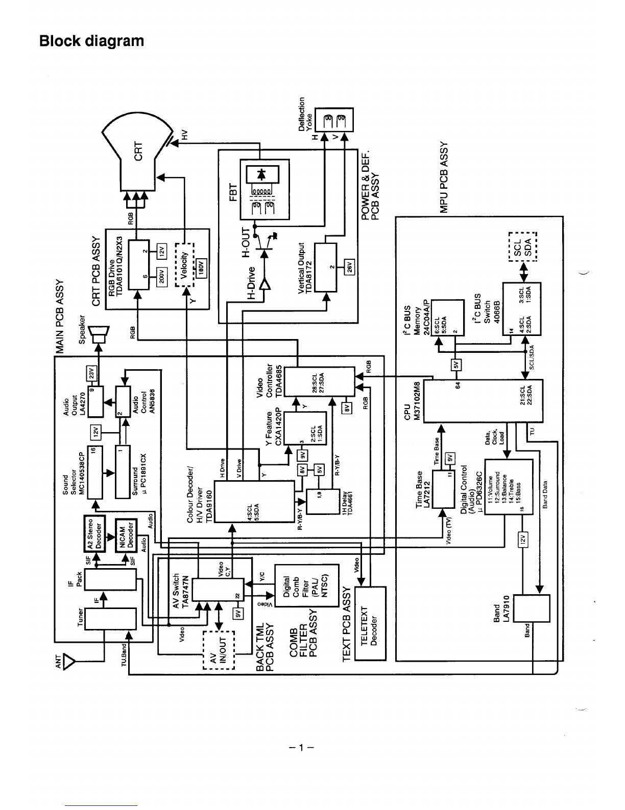
1-1. Video signal routing
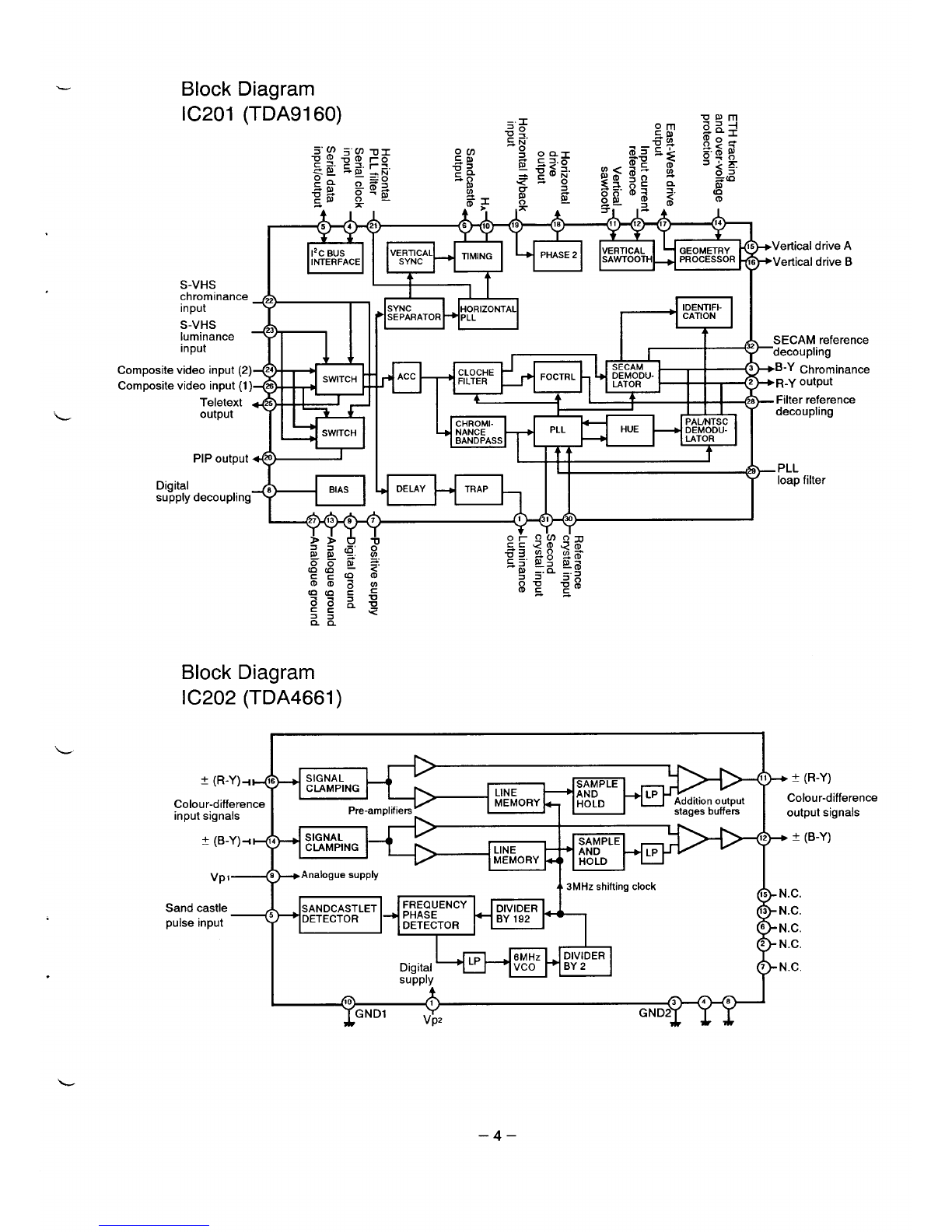
Video signals output from IF pack are input to AV
switching IC (TA8747N). In this IC, they are switched to
AV signals. Colour. Yor composite signals output from
TA8747N are input to Colour Decoder &H/V Drive IC
(TDA91 60) and Ysignal is input to the Teletext Decoder.
All functions of TDA9160 are controlled by I’C Bus lines
(SCL:Serial Clock/ SDA:Serial Data) of CPU. Ysignal
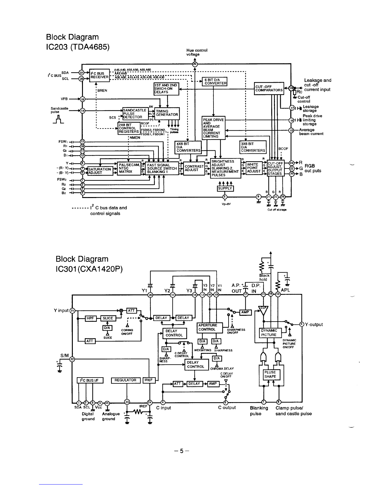
output from TDA9160 is input to YFeature IC (CXA
1420P) for the aperture control and black expand and
input to the velocity circuit. Ysignal output from CXA
1420P is input to Video Controller IC (TDA4685). Colour
differential signals (R- Y/B- Y) demodulated byTDA9160
are input to 1Hdelay IC (TDA4661 )as 1Hdelay and
matrix and output to TDA4685 as proper colour
differential signals. In TDA4685, colour differential signals
are converted to RGB signals, RGB signals from Teletext
decoder or CPU are super- imposed on them, and RGB
signals are output to RGB Drive IC (TDA6101 Q/N2). C)(A
1420P and TDA4685 also are controlled by I*C Bus lines.
1-2. Audio signal routing
SIF signals output from IF pack are input to A2 stereo
decoder and NICAM stereo decoder. Stereo signals
detected by both decoders are input to AV switching
IC(TDA8747N). After switching to external audio signals
in this IC, they are input to Sound Selector IC
(MC140538CP) as selecting an L channel, an Rchannel
or both channels. Audio signals output from MC
140538CP are input to the Surround IC as mixing
surround signals in surround mode. Output signals are
input to Audio Control IC (AN5836). Bass, treble,
balance and volume control is applied to signals, which
are amplified by Audio Output IC (LA4720), and output to
the speakers.
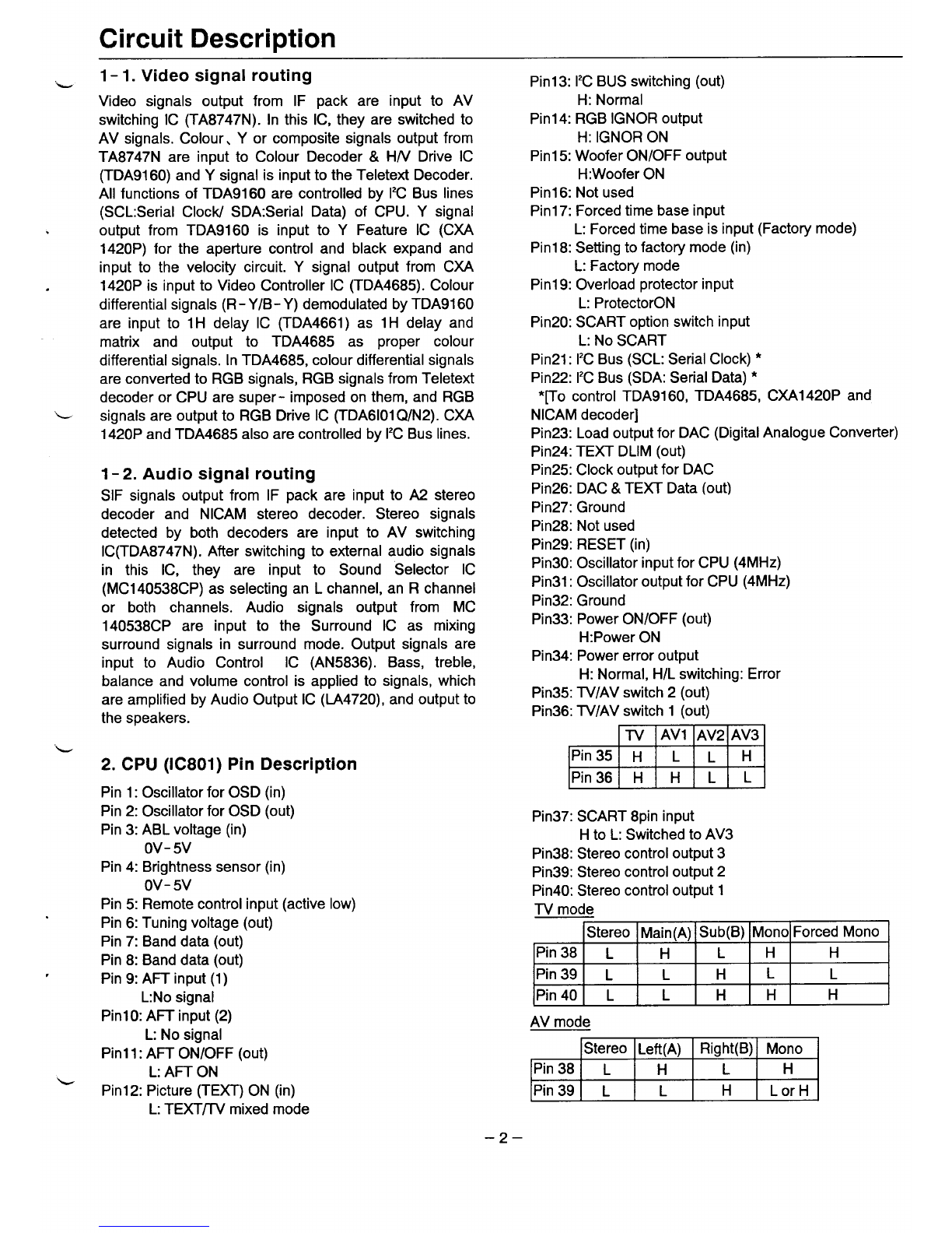
2. CPU (IC801) Pin Description
Pin 1: Oscillator for OSD (in)
Pin 2: Oscillator for OSD (out)
Pin 3: ABL voltage (in)
Ov- 5V
Pin 4: Brightness sensor (in)
Ov- 5V
Pin 5: Remote control input (active low)
Pin 6: Tuning voltage (out)
Pin 7: Band data (out)
Pin 8: Band data (out)
Pin 9: AFT input (1)
L:No signal
PinlO: AFT input (2)
L: No signal
Pinl 1: Am ON/OFF (out)
L: AFT ON
Pinl 2: Picture (TEXT) ON (in)
L: TEXT/lV mixed mode
–2–
Pinl 3: 12CBUS switching (out)
H: Normal
Pin14: RGB IGNOR output
H: IGNOR ON
Pinl 5: Woofer ON/OFF output
H:Woofer ON
Pinl 6: Not used
Pinl 7: Forced time base input
L: Forced time base is input (Factory mode)
Pinl 8: Setting to factory mode (in)
L: Factory mode
Pinl 9: Overload protector input
L: ProtectorON
Pin20: SCART option switch input
L: No SCART
Pin21: I*C Bus (SCL: Serial Clock) *
Pin22: 12C Bus (SDA: Serial Data) *
‘To control TDA91 60, TDA4685, CXA1420P and
NICAM decoder]
Pin23: Load output for DAC (Digital Analogue Converter)
Pin24: TEXT DLIM (out)
Pin25: Clock output for DAC
Pin26: DAC &TEXT Data (out)
Pin27: Ground
Pin28: Not used
Pin29: RESET (in)
Pin30: Oscillator input for CPU (4MHz)
Pin31: Oscillator output for CPU (4MHz)
Pin32: Ground
Pin33: Power ON/OFF (out)
H:Power ON
Pin34: Power error output
H: Normal, H/L switching: Error
Pin35: TVIAV switch 2(out)
Pin36: TV/AV switch 1(out)
Tv AVI AV2 AV3
lPin 35 HLLH
lPin361Hl HILl L
Pin37: SCART 8pin input
Hto L: Switched to AV3
Pin38: Stereo control output 3
Pin39: Stereo control output 2
Pin40: Stereo control output 1
TV mode
Stereo Main(A) Sub(B) Mono Forced Mono
Pin 38 LHLHH
Pin 39 LLHLL
Pin 40 L L HHH
AV mode

Circuit Description
Pin41: Switch for S- VHS (in)
H: S- VHS mode (Y/C separated mode)
Pin42: Skew output
H: Skew ON
Pin43: A2 stereo data input 1
Pin44: A2 stereo data input 2
Stereo Bil. Mono Forced Mono
Pin43 HL L H
Pin44 LHLH
Pin45: Sound mute (out)
Pin46: Line mute (out)
H: Mute ON
Pin47: Option switch scan output 3
Pin48: Option switch scan output 2
Pin49: Option switch scan output 1
Pin50: Key scan output 3
Pin51: Key scan output 2
Pin52: Key scan output 1
Pin53: Key scan input 4
Pin54: Key scan input 3
Pin55: Key scan input 2
Pin56: Key scan input 1
Pin57: OSD (On Screen Display) banking output
Pin58: Not used
Pin59: OSD blue output
Pin60: OSD green output
Pin61: OSD red output
Pin62: Vertical synchronisation pulse input for OSD
Pin63: Horizontal synchronisation pulse input for OSD
Pin64: Power supply (+5V)
3. DAC (IC809) Pin Description —
Pinl: Power supply (+5V)
Pin2: Data input from CPU (Pin26)
Pin3: Clock input from CPU (Pin25)
Pin4: Load input from CPU (Pin23)
Pin5: Surround ON/OFF output
H: Surround ON
Pin6: Not used
Pin7: SIF System(M) output
Pin8: Ground
Pin9: SIF System (1)output
Pinl O:SIF System (B/G, D/K) output
AUTO BIG D/K INTSC4.43
Pin 7LHLHH
Pin 9L L HLL
Pinl OL L I-i HH
Pinl 1: Volume output
Pin12: Surround level output
Pinl 3: Balance output
Pinl 4: Treble output
Pinl 5: Bass output
Pinl 6: Power supply (+5V)
.4
–3–

Block Diagram
L
‘L
IC201 (
drive A
drive B
S-VHS
chrominance
input
S-VHS
luminance
input reference
ing
Composite video input (2
. . ....+/4
Composite video inPU, ~I) -
B
Teletext b
output
SWITCH
PIP output
1ID-1 Chromlflance
JR-y OUtpUt
Filter reference
decouphng
PI I
.uonlvdecouolina_ ~I~i’;fi’ter
Digital
Block Diagram
IC202 (TDA4661 )
ifference
gnals
s
P
L
–4–

Block Diagram
IC203 (TDA4685) Hue control
voItage
M5.MO, #.s.iAse,A65.IW3
SDA
12CBUS -u5x4a--------------------------
...............................,
SCL Ac5.AlxtA15.Am,M.Am, A25.A3U
.............................. 1
4,,
m
ISTAND2ND ;
:BREN SWICH-ON
DELAYS
VFE
....................
Leakage and
cut -off
~current input
11’7(
BCOF
1ST,
iES
R
Sandcastle BK 4+
pu15e SANOCASTLE
m,,, or 1)1F&:~mye’
Peak driie
ti I-& limiting
storage
PEAK DRIVE
AND
AVERAGE
BEAM 4
CURRENT
LIMITING
w4
n
3X6 BIT
O/A
CONVERTERS
eAverage
beam current
RI ++@) ,1:
4m
v
I
v
-(R-Y)+
G2-1
I~I
B
SUPPLY
------- 12 Cbusdata and !offstorage
control signals
1
+
Bac
hold
T
A.P. +D.P.
OUT% IN .. ,.
Block Diagram
IC301 (CXAI 420P) ri
APL
.,.
),-output
W%=+k==!i! w
‘m“LA”=x+.J43Cinput cOutmlt Blanking Clamp pulse/
Digital Analogue pulse sand castle pu Ise
greund ground xx
–5–

Service control adjustments
w
.
.
L
L
.
.
\
SAFETY PRECAUTIONS :An isolation transformer should be connected in the power line between the receiver and the AC
line before any service is performed on the receiver.
X-RADIATION PRECAUTION The primary source of X-RADIATION in television receiver is the picture tube. The picture
tube is specially constructed to limit X-RADIATION emission. For continued X-RADIATION protection, the replacement tube must
be the same type as the original including suffix letter. Excessive high voltage may produce potentially hazardous X-RADIATION.
To avoid such hazards, the high voltage must be maintain within specified limit, Refer to this service manual for specific high
voltage limits. If high voltage exceeds specified limits, take necessary corrective action. Carefully follow the instructions for +B1 volt
power supply adjustment, and high voltage check to maintain the high voltage within the specified limits.
(1) Receive the PAL colour bar pattern, (1) Receive the monochrome circular pattern.
(2) Set the brightness and contrast to normal.
g(3) Vertical centering can be adjusted by switching SW501 on
a) gc:
ca~the POWER &DEF PCB ASS’Y.
.= =
$ $ $ 6 g z:pAL colour
bar pattern
x
v:$:
3%
ummca’cen’er
II I I 1I
(2) Connect the oscillator to Q1 33- Emitter on the MAIN PCB
ASS’Y.
(3) Adjust VR131 for 1.OVP- pas shown below.
@
Video det. T
waveform
1
3
0
0
u
o
I.Ovp-p
L
VIDEO
DET, ADJ.
i
❑
~VR131
OQ133
\Emitter
uMAIN PCB ASS’Y
POWER &DEF. PCB ASS’Y
(1) Receive the monochrome circular pattern,
(2) Set the brightness and contrast to normal.
(3) Adjust VR2301 on the SYNC SUB PCB ASS’Y for optimum
horizontal center position.
~orizontal center
(1) Connect the high voltage probe(+) to the anode lead of the
picture tube and the ground.
(2) Receive the monochrome circular pattern.
(1) Receive the monochrome circular pattern.
(2) Set the brightness to normal and contrast to maximum.
(3) Adjust the focus control on the F.B.T for the best focus on (3) Set the brightness and contrast to minimum.
the screen center. (4) The high voltage must be less than 25’’=3OKV, 29’’=32.5
Kv.
– 6 – Note: If the picture tube is replaced, check the high voltage.

Service control adjustments Tuner assembly adjustments
(1) Receive the PAL colour bar pattern.
PAL colour
bar pattern
(2) Connect the oscillator to TP -Y(+) and TP -E( - ) on the
COMB FILTER PCB ASS’Y.
(Oscilloscope sens. ~0.2V/div)
COMB FILTER PCB ASS’Y VR2801
/
\
~02001
00 .......
K78CM
1.. 00
0o
8TP-Y
(3) By using VR2801 on the COMB FILTER PCB ASS’Y,
adjust the amplitude as shown below.
0.05 Vp-p
The following components of Tuner Assembly (645 000 1192) _
can be ordered separately:
Tuner Ass’y (645 0001192)
Ref. No. Part No. Description
AlolA 6450001208 UV Varactor Tuner
IA101B 6450005312 IF Pack 1
+When you order these components together as the Tuner
Assembly, they do not need to be adjusted.
●Since each components is pre -adjusted at the time of
shipment, it does not usually require further adjustment, even
when purchased separately. However, if there is any such
need, you can follow the instructions below to perform the
adjustment.
AGC Adjustment
Note: Do not attempt this adjustment with the weak signal.
(1) Tune the receiver to the most clearest (or strongest) VHF _
station in your area,
Set the brightness and the contrast to maximum.
Set the colour to minimum.
(2) Turn the AGC control (SVR101 )of the IF Pack in direction
which causes the snow to armears, then in opposite
direction until the snow just disappears.
>
0
0
0
Q1
+
BQ133
%AGC Adjustment
MAIN UNIT
–7–

w
.
L
L
.
.
‘L
Adjustments in the Service mode
Since some chassis circuit adjustments are controlled by the CPU built into the chassis, adjustments can now be made
by inputting data directly via the remote control unit supplied with the set.
Memory IC (lC805)replacement
Since adjustment data for the circuit is stored in the memory IC (IC805) that comes with the CPU, the adjustment data
must be re- input when the memory IC is replaced.
(After memory IC replaced, reference data is initially written automatically to memory from the CPU ROM for basic set
operation.)
(1) setting of the service mode.
To enter service mode. mess and hold down the MEMORY key on the front control panel of the TV set, then press the remote
control Normalization key.
~j-- o p F-+ -+
\MEMORY key
(2) Screen display in the service mode.
–Screen display –
ITEM DATA
01.v-s 15
\.
Item o<the ~djustments data
adjustments
A-45=i=-’”i=
AIB SURROUND Fuzzv
‘zw=’8E
~1%~
w
+u.u-&-~
o-J-
Dlm&&
IL’ I
-Normalization
key
(Remote Control Transmkter)
Epy
VPA Prog. UP/DOWN
—LEVEL
}
AIB SURROUND FUZZY
00
●Item of the adjustments can be selected by
pressing Prog. UP/DOWN (7P A )key of the
remote control unit.
.Adjustments data can be set by pressing LEVEL
(-~ +) key of the remote control unit.
See the next page for adjustment items and data.
(3) Reset of the service mode.
To exit from the service mode, turn off the TV set by pressing the Power ON/OFF button of the TV set or the remote control
transmitter.
–8–

Adjustments in the Service mode
The displayed data is not post adjustment data, but initial reference data from the CPU ROM for basic set operation
following memory IC replacement. Perform individual adjustments according to the circuit adjustment method described
earlier when the memory IC is replaced.
–Table of the adjustments –
Screen Display Data
Adjustments Range of a
PAL NTSC data Remarks
01.v-s Vertical Shift Adjustment 31 31 00 – 63 Not used
1
02. V-A Vertical Size Adjustment 34 I34 I00 – 63 I
03. V-L Vertical Linearity Adjustment 31 31 00 – 63
~04. s-c S-Correction Adjustment 31 31 00 – 63
05. H-S Horizontal Center Adjustment 00 00 00 – 63 Not used
06. H-W IHorizontal Width Adjustment I37 I38 I00-63 II
07. P-w Pincushion Adjustment (Parabola width) 28 29 00 – 63
08. C-P Pincushion Adjustment (Corner parabola) 31 25 00 – 63
~09. TRP Pincushion Adjustment 25 I20 00 – 63
10. RRed Gain Adjustment 24 00 – 63
11. GGreen Gain Adjustment 24 00 – 63
12. BBlue Gain Adjustment 24 00 – 63
~13. P-L Peak Drive Limit Adjustment 45 00 – 63
~14. S-L Slice Adjustment 10 00 – 63
~15. S-F Sharpness Focus Adjustment 20 00 – 63
~16. W-H Weighting Adjustment 21 00 – 63
17. C-D Chroma Delav Adjustment 31 00 – 63 Not used
I. . 11,
18. OSD On Screen Display Center Adj. 7 00 – 63
Note: In the event that separate data adjustments are required, such as for PAL and NTSC systems, perform individual
adjustments for PAL and NTSC signal reception.
Adjust for NTSC by inputting the NTSC signal from the AV input terminal.
(1) Connect the oscilloscope to TP -47G and the ground(TE -
47) of the CRT PCB ASS’Y.
(2) Receive the PAL colour bar pattern.
(Set the colour control to minimum and the contrast to
maximum.)
PAL colour
bar pattern
(3) Adjust the brightness control volume to be a=l OV *; V.
Tir
a
T
i’
(4) Set the TV re!%ver to the service mode.
(5) Select”1 1. G“ by pressing Prog. UP/DOWN key.
(6) Adjust so that b=85 Vf3V by pressing LEVEL (- ~ + )key.
Note: This adjustment should be done after sub contrast
adjustment.
(1) Receive the PAL monochrome circular pattern.
(Set the colour and brightness control to normal and the
contrast to maximum.)
(2) Set the TV receiver to the service mode.
(3) Select”1 O. R“ by pressing Prog. UP/DOWN key, and adjust
so that the red gain is optimum level by pressing LEVEL (-
~ + )key.
(4) Select”1 2. Bby pressing Prog. UP/DOWN key, and adjust
so that the blue gain is optimum level by pressing LEVEL
(-~ +)key.
(1) Receive the monochrome circular pattern.
(Set the brightness to normal and contrast to maximum.)
(2) Set the TV receiver to the service mode.
(3) Select “02. V-A by pressing Prog. UP/DOWN key of the
remote control unit.
(4) Adjust the vertical size by pressing LEVEL (- ~ + )key.
–9–

Adjustments in the Service mode
(1) Receive the monochrome circular pattern.
(Set the brightness to normal and contrast to maximum.)
(2) Set the TV receiver to the service mode.
(3) Select “03. V- L“ by pressing Prog. UP/DOWN key.
(4) Adjust the vertical linearity by pressing LEVEL (-~+) key.
QQT
Q<L.A. ./’<
‘l. _/.~
w‘1
QVertical linearity (lower)
(1) Receive the monochrome pattern.
(Set the brightness to normal and contrast to maximum.)
(2) Set the TV receiver to the service mode.
b(3) Select “06. H-W by pressing Prog. UP/DOWN key.
(4) Adjust the horizontal width by pressing LEVEL (-~+) key.
(1) Receive the grid pattern.
(Set the brightness to normal and contrast to maximum.)
(2) Set the TV receiver to the service mode.
(3) Select “07. P-W“(Parabola width) by pressing Prog.
UP/DOWN key.
(4) Adjust so that the vertical line is straight by pressing LEVEL
(-~ +)key.
Parabola width
adjustment
(5) Select “08. C-P“(Corner parabola) by pressing Prog.
UP/DOWN key.
(6) Adjust so that the vertical line is straight by pressing LEVEL
(-~ +)key.
Corner parabola
adjustment
.
Adjustmentsmarked with an asterisk (“X)in
the summary display are difficult to adjust
visually, so be sure to reset using the displayed
data only if the setting differs from that
displayed.
(1) Receive the monochrome circular pattern.
(Set the brightness and contrast to normal.)
(2) Set the TV receiver to the service mode.
(3) Select”1 8.OSD 05” by pressing Prog. UP/DOWN key.
(4) Adjust so that the tuning bar center is optimum position by
Lpressing LEVEL (- - +)key.
–lo–

PURITY AND CONVERGENCE ADJUSTMENT
CAUTION:The Convergence and Purity adjustments have been made at the factory. Readjustment should be
made only after picture tube or deflection yoke replacement, following the steps below:
PURITY ADJUSTMENT
1.Demagnetize the picture tube and receiver using an external
degaussing coil. When replacing picture tube or deflection
yoke, mount deflection yoke and purity -convergence
magnets assembly properly, see figures 1 and 4.
2.Turn Red and Blue guns off and provide only Green raster.
Rotate Screen control to fully counterclockwise. Rotate Red
and Blue Bias controls fully counterclockwise. Slowly rotate
Green Bias control clockwise to produce Green raster.
3.Loosen the screw holding the Deflection Yoke and remove
the 3Rubber Wedges, and slide the Deflection Yoke fully
frontward.
4. Rotate and spread the Tabs of the two Purity Magnets to
center the vertical green belt in the picture screen. The Purity
Magnets are also adjusted to obtain vertical centering of the
raster.
5.Slowly slide the Deflection Yoke backward until auniform
green screen is obtained.
6.Check the purity of the red and blue screens for uniformity,
turn off other colours to check this (use bias controls).
Readjust the yoke position if necessary until all screens are
pure.
7,Adjust each Bias control and screen control to obtain white
8. Tighten the mounting screw of the Deflection Yoke. Adjust
Convergence next.
CENTER CONVERGENCE ADJUSTMENT
1, Use adot crosshatch pattern signal.
2. Turn Red and Blue guns on and turn off Green gun. Adjust
the angle between the Tabs of the Four Pole Magnet 1and
2,and superimpose the Red and Blue vertical lines in the
center area of the picture screen. Refer to figure 2.
3. Keeping the mutual angle of the Tabs of the Four Pole
Magnet turn them together to superimpose the Blue and Red
horizontal lines in the center area of the picture screen. Refer
to figure 2.
4. Turn Green gun on and adjust Six Pole Magnet 3 and 4sthat
the Green line superimposed on the Red/Blue lines.
This is the same procedure used in steps 2and 3.
Refer to figure 3.
OUTER AREA CONVERGENCE ADJUSTMENT
Slightly loosen the screw holding the Deflection Yoke. Adjust
the Deflection Yoke to converge the detail in the outer area (left
side and right side) of the picture screen by orbital movement of
the front of the Yoke, then secure the Deflection Yoke in
raster, Refer to Gray Scale Adjustment. If part of the picture appropriate position by putting the wedges as illustrated.
screen is coloured, adjust the Deflection Yoke position Tighten screw holding the Deflection Yoke.
forward or backward slightly.
DEFLECTION YOKE
FOUR- POLE
MAGNET TABS
rx SIX- POLE
~AGNET TABS
Figure- 1. PURITY AND CONVERGENCE MAGNETS Figure- 4. ADJUSTMENT DEFLECTION YOKE
Adjust tabs angle to superimpose
blue and red vertical line
J
RED Adjust tabs together to
+
I_ superimpose red and
\___ ~___ L/ blue horizontal line
BLUE
Adjust tabs angle to superimpose
red/blue and green vertical line
IAdjust tabs together to
+
GREEN
/
superimpose red/blue
\--- :__l_ and green horizontal line
BLUE/RED
Figure- 2BLUE AND RED LINE MOVEMENT IFigure-3 BLUE/RED AND GREEN LINE MOVEMENT
–11–

I
~CABINET PARTS LIST
Note :Parts order must contain Service Ref. No., Key No., Parts No., and Description.
IIII 11 II
II \II
i!11 \JI
17
/14 16
\J
SANYO
1..1 IALlo-
1IQI‘Prow
,L(
/—
/
I
10 I
‘‘1 \/iw
/
II
II
9876 ‘5 4’ ,!~ ‘1 v-lb -
/
15
‘ey Part No. Description ‘ey Part No.
No. No. IDescription
1. 610 235 5062 BUTTON 13. 6102393828 KY. DEC BOARD TOP
2. 6102131437 COIL SPLING 14. 610 244 7569 CABINET 8ACK
.— —.. —-.-.
3. 6102395013 SHAFT (for AC SWITCH) 15. 610 240 2315 DEC REAR SHEET _—.—
4. 6102447552 ASSY. DEC BOARD LATCH 16. 610 2447477 LABEL RATING
5. 6102353389 DOOR 17. fjl () 2404470 RC TRANSMITTER JXHS
6. 6102097191 PUSH LATCH
...—.- .-
7. 610 2447354 DEC CONTROL SHEET
8. 6102228151 DAMPER
9. 6102447811 ASSY. DEC BOARD LEFT ——. —------
-..
10. 610 244 7828 /& DECBOARDFRO/IJT
1; 610 236 9274 SANYO BADGE
.—..—
12. 610 235 8278 ASSY CABINET
——
–12–

E6TV
CHASSIS ELECTRICAL PARTS LIST
Product safety should be considered when acomponent replacement is made inany area ofa receiver.
Components indicatedby a A mark inthispartslistand the circuitdiagram show components whose value have
specialsignificancetoproductsafety.Itisparticularlyrecommended thatonlypartsspecifiedon thefollowingparts
listbe used forcomponents replacementpointedoutby the mark.
Note:PartordermustcontainServiceRef.
No.,Parl No,.and descri~tions. The main PCB unit will be sutmlied without tuner and
flyback transformer. They shouldbe orderedseparately. ––-,
,
Read description in the Capacitor and Resister as folfows
CAPACITOR
CERAMIC
T
K50V
L~Rated Voftage
ToIerance Svmbels
Less than lbPF
A: Not specxhed B:*o,l PF
D: ~0.5PF F+l PF
R: +0,25-OPF S: +0-0,25PF
More than 10PF
?+:Not speafled B*0.1%
D: *0.5% F+l%
H: f3% J:~5%
L: f15% M: +20%
P+100-0% Q: +30- 10%
u: +75- 10% w+20-10%
x: +40- 20% Y +150-10%
J.a, LRated value: P.pica farad, U. Micro fared
CER’AMIC .............Ceramic
MT- PAPER..,...,... Metallized Paper
POLYESTER,... Polyesterester
MT- PO LYEST ......Metallized Polyester
POLYPRO,,.,..,.., Poiypropyleneene
MT- PO LYPRO .....Metallized Polypropylene
COMPO FILM ........Composite film
MT- COMBO,.,,..,., Metallized Cmposite
STYRENE., . .........Styrene
TA-SOLID.,, .........Tantalum Solid
AL- SOLfD ............Aluminium Solid
ELECT ..................Electrolytic
NP-ELECT ...........Non-polanzed Electroiytii
OS- SOLID..., .......Aluminium Solid with Organic
Semiconductive Electrolytic
DL- ELECT ...........Double Layered Electrolytic
RE
CA
—
Ma
TER
~:
ial :
A1/4W
r-f-
C: f0.25PF
G: f2PF
E: +0-l PF
N: +30%
T: +50- 10%
w: +100-10%
z: +80- 20%
LLRated Wattage
Performance Symbols
A:General B:Non flammabie 2LOW noise
Other :Tempereture ceeffident
‘Tolerance Symbols:
A: f0.05% B: *0.1% C: ~0.25% Df0.5%
F: k1% G: ~2% J: ?5% K*10%
M: +20% P+5-15%
—Rated value, ohms:
K1 ,000, M:l ,000,000
CARBON ............Carbon
MT- FILM................Metal Film
OXIDE-MT ........Oxide Metal Film
SOLID ..................Composition
MT-GLAZE ..........Metal Glaze
WIRE WOUND .......whe Wound
CERAMIC RES .......Ceramic
FUSIBLE RES ........Fusible
Ref.No. PartNo. Description
6102450446 SUB PW PCB ASSY E5YV UE2570B
TRANSISTER
fl1521 4050148408 TR 2SC2568(1)-K
4050148507 TR 2SC2568(1)-L
405041 6507 TR 2SC2621-D-RA
405041 6705 TR 2SC2621-E-RA
CAPACITOR
AC1511 4040575702 MT-COMPO O.22U M 250V
C1513 4040575702 MT-COMPO O.22U M 250V
C1514 4040082705 CERAMIC 470P K 400V
C1515 4040082705 CERAMIC 470P K 400V
C1516 4030767100 CERAMIC 1000P M lK
C1517 4030767100 CERAMIC 1000P.M 1K
C1518 4030767100 CERAMIC 1000P M lK
C1519 4030767100 CERAMIC 1000P M lK
C1521 4030541502 ELECT 470U M 35V
RESISTER
R1501 4020586605 WIRE WOUND 3.9 JA 15W
R1522 401 0604104 OXIDE-MT 2.2K JA lW
TRANSFORMER
AT1501 6100333758 POWER TRANS
6102404722 POWER TRANS
COIL
L1511 610031 6171 LINE FILTER
AL1512 610031 6171 LINE FILTER
DIODE
D1511 4070066300
4070646908
D1512 4070066300
4070646908
D1513 4070066300
4070646908
D1514 4070066300
4070646908
D1522 4070057308
D1525 4070482001
01ODE ERC05-108
D10OETVR4N(X)
DIODE ERCO5-1OB
DiODE TVR4N(X)
DIODE ERCO5-108
D100ETVR4N(X)
D10DEERCO5-108
DIODE TVR4N(X)
DIODE EMOIZ
ZENER DIODE EOA02-06B
MISCELLANEOUS
AF1511 4230072103 FUSE 250V 4A
PS1511 4080133801 TH PTH451C2628F140M270
610240 1004 TEXT PCB ASSY E5YY UE2573
TRANSISTER
01031 4060072106 TR JC546A
4060072007 TR JC546B
4050191909 TR 2SC536-E-NP
4050192708 TR 2SC536-F-NP
4050193804 TR 2SC536-G-NP
—13—

E6TV
b
L
L
.
.
‘L
Ref. No. IPart No. IDescritXion
01032
01033
01041
01050
01052
4060072106
4060072007
405019 1909
4050192708
4050193804
4060072106
4060072007
4050191909
4050192708
4050193804
4060072106
4060072007
4050191909
4050192708
4050193804
406007 1901
406007 1802
4050044205
4050044809
4050287909
4060072106
TR JC546A
TR JC5468
TR 2SC536-E-NP
TR 2SC536-F-NP
TR 2SC536-G-NP
TR JC546A
TR JC546B
TR 2SC536-E-NP
TR 2SC536-F-NP
TR 2SC536-G-NP
TR JC546A
TR JC546B
TR 2SC536-E-NP
TR 2SC536-F-NP
TR 2SC536-G-NP
TR JC556A
TR JC556B
TR 2SA608-E-CTV-NP
TR 2SA608-F-CTV-NP
TR 2SA608-G-CTV-NP
TR JC546A
4060072007 TR JC546B
405019 1909 TR 2SC536-E-NP
4050192708 TR 2SC536-F-NP
4050193804 TR 2SC536-G-NP
INTEGRATEDCIRCUIT
Icloll
IC1031
IC1032
IC1051
ICI052
IC1053
IC1054
IC1055
:APACITOR
Cloll
C1012
C1OI3
C1014
C1016
C1017
C1018
C1019
C1021
C1022
4091078108
4101175100
410051 0506
4101096603
4090127708
409 1667302
409 143 1705
4091204101
4090896000
4091631501
409 1204200
4090896109
409 1631402
4090734906
409 1627504
409 1627405
4090543706
409 1387705
4100395905
4092588309
4091850100
4091849906
4090507906
4091848909
4100673102
4090206601
4090507807
4090206908
4090508309
4030698305
4030439106
4030197709
4030124309
4030093407
4030724400
4030595000
4030595703
403 1792507
4030736403
4030690507
4030124309
IC SAA5231
IC SM5231/V7
IC SM5243P/E-M2
IC SAA5243P/E-M3
IC HM6264P-15
IC LC3564P-15
IC LC3564PL-15
IC LC3664N-10
IC LC3664N-12
IC LC3664N-85
IC LC3664NL-10
IC LC3664NL-12
IC LC3664NL-85
IC TC5565PL-15
IC TMM2064AP-10
IC TMM2064AP-12
IC TMM2064P-10
IC UPD4364C-15
IC MAB8461PW115
IC 85C72/P
IC MC14006B
IC MN4006B
IC TC4006BP
IC UPD4006BC
IC HEF4006B
Ic LC4001B
Ic TC4001BP
Ic LC4011B
Ic TC4011BP
CERAMIC
ELECT
CERAMIC
CERAMIC
CERAMIC
CERAMIC
POLYESTER
POLYESTER
POLYESTER
CERAMIC
CERAMIC
CERAMIC
O.olu z 50V
47UM 16V
27PJ 50V
15PJ 50V
100PJ 50V
270P K 50V
0.022U J 50V
0.022UJ 50V
0.022UJ 50V
470P K 50V
1000P K 50V
15PJ 50V
Ref. No. IPart No. IDescription
C1023
C1024
C1025
C1026
C1027
C1028
C1029
C103O
C1031
C1032
C1033
C1051
C1052
C1053
C1054
C1056
C1061
C1062
RESISTER
R1011
R1012
R1013
R1014
R1016
R1017
R1031
R1032
R1033
R1034
R1036
R1037
R1038
R1039
R1041
R1042
R1043
R1044
R1051
R1052
R1053
R1054
R1055
R1056
R1057
R1058
R1059
R1061
R1062
R1063
R1064
R1066
R1067
R1068
R1069
R107O
4030678208
403071 5606
4030865400
4030677706
4030439106
4030677706
4030677706
4030698305
4030675603
4030439106
4030439106
4030225907
4030225907
4030698305
4030430202
4030698305
403071 7402
4030745702
401 0246700
401 0249305
401 0246700
401 0275908
401 0278107
401 0264308
401 0257805
401 0264308
401 0257805
401 0257805
401 0264308
401 0257805
401 0257805
401 0264308
401 0257805
401 0275908
401 0264308
401 0276608
401 0279005
401 0269907
401 0247400
401 0272303
401 0248001
401 0254200
401 0269600
401 0269600
401 0269907
401 0269600
401 0247400
401 0269907
401 0269907
401 0247400
401 0247400
401 0247400
401 0247400
401 0257805
MT-COMPO
CERAMIC
NP-ELECT
MT-COMPO
ELECT
MT-COMPO
MT-COMPO
CERAMIC
MT-COMPO
ELECT
ELECT
CERAMIC
CERAMIC
CERAMIC
ELECT
CERAMIC
CERAM1C
CERAMIC
CARBON
CARBON
CARBON
CARBON
CARBON
CARBON
CARBON
CARBON
CARBON
CARBON
CARBON
CARBON
CARBON
CARBON
CARBON
CARBON
CARBON
CARBON
CARBON
CARBON
CARBON
CARBON
CARBON
CARBON
CARBON
CARBON
CARBON
CARBON
CARBON
CARBON
CARBON
CARBON
CARBON
CARBON
CARBON
CARBON
0.068U J
220P K
2.2U M
0.047U J
47U M
0.047U J
0.047U J
O.olu z
O.lU J
47U M
47U M
33P J
33P J
O.olu z
220U M
O.olu z
2200P K
560P K
100 JA
1.2K JA
100 JA
68K JA
82 JA
3.3K JA
2.2K JA
3.3K JA
2.2K JA
2.2K JA
3.3K JA
2.2K JA
2.2K JA
3.3K JA
2.2K JA
68K JA
3.3K JA
75 JA
82K JA
4.7K JA
10K JA
560 JA
lM JA
1.8K JA
470 JA
470 JA
4.7K JA
470 JA
10K JA
4.7K JA
4.7K JA
10K JA
10K JA
10K JA
10K JA
2.2K JA
50V
50V
50V
50V
16V
50V
50V
50V
50V
16V
16V
50V
50V
50V
16V
50V
50V
50V
1/6W
1/6W
1/6W
1/6W
1/6W
1/6W
1/6W
1/6W
1/6W
1/6W
1/6W
1/6W
1/6W
1/6W
1/6W
1/6W
1/6W
1/6W
1/6W
1/6W
1/6W
1/6W
1/6W
1/6W
1/6W
1/6W
1/6W
1/6W
1/6W
1/6W
1/6W
1/6W
1/6W
1/6W
1/6W
1/6W
TRANSFORMER
T1011 6100377547 S TRANS
toll
----
L1011 6100295346 PEAKING COIL
L1012 6100295476 PEAKING COIL 4.7UHK
L1031 6100295575 PEAKING COIL 1.5UHM
L1032 6100295575 PEAKING COIL 1.5UHM
L1041 6100295575 PEAKING COIL 1.5UHM
DIODE
D1051 4070125809 DIODE 1SS176
D1052 4070125809 DIODE 1SS176
—14—

E6TV
Ref. No. Part No, Description
D1053 4070557907 ZENER DIODE RD3.6EL
lISCELLANEUS
Xloll 6100121706 CRYSTALOSCILLATOR
610211 4218 CRYSTALOSCILLATOR
610211 6458 CRYSTAL OSCILLATOR
X1051 6102246346 CERAMIC OSCILLATOR KBR-6.
6100120563 CERAMIC OSCILLATOR
610 245 3904 CRT & VM PCB ASSY E6TY UE2574A
TRANSISTER
01701
01702
01703
01705
01706
01707
4060006804 TR 2SA1015-GR(SAN)
405001 7407 TR 2SA1015-0(SAN)
405001 7605 TR 2SA1015-Y(SAN)
4050043109 TR 2SA564A-O(CU)
4050043208 TR 2SA564A-R(CU)
4050044205 TR 2SA608-E-CTV-NP
4050044809 TR 2SA608-F-CTV-NP
405006 1103 TR 2SA933-11
4050061202 TR 2SA933-R
405011 7305 TR 2SC1740-(1
405011 7404 TR 2SC1740-R
405011 7503 TR 2SC1740-S
4050122002 TR 2SC1815-GR
4050122101 TR 2SC1815-O
4050122309 TR 2SC1815-Y
405019 1909 TR 2SC536-E-NP
4050192708 TR 2SC536-F-NP
4050193804 TR 2SC536-G-NP
4050207501 TR 2SC945A-PA
4050207709 TR 2SC945A-OA
4050207907 TR 2SC945A-RA
405011 7305 TR 2SC1740-O
405011 7404 TR 2SC1740-R
405011 7503 TR 2SC1740-S
4050122002 TR 2SC1815-GR
4050122309 TR 2SC1815-Y
4050192708 TR 2SC536-F-NP
4050193804 TR 2SC536-G-NP
4050207501 TR 2SC945A-PA
4050207709 TR 2SC945A-OA
405011 7305 TR 2SC1740-O
405011 7404 TR 2SC1740-R
405011 7503 TR 2SC1740-S
4050122002 TR 2SC1815-GR
4050122101 TR 2SC1815-O
4050122309 TR 2SC1815-Y
405019 1909 TR 2SC536-E-NP
4050192708 TR 2SC536-F-NP
4050193804 TR 2SC536-G-NP
4050207501 TR 2SC945A-PA
4050207709 TR 2SC945A-OA
4050207907 TR 2SC945A-RA
405011 7305 TR 2SC1740-O
405011 7404 TR 2SC1740-R
405011 7503 TR 2SC1740-S
4050122002 TR 2SC1815-GR
4050122101 TR2SC1815-O
4050122309 TR 2SC1815-Y
405019 1909 TR 2SC536-E-NP
4050192708 TR 2SC536-F-NP
4050193804 TR 2SC536-G-NP
4050207501 TR 2SC945A-PA
4050207709 TR 2SC945A-OA
4050207907 TR 2SC945A-RA
405011 7305 TR 2SC1740-O
405011 7404 TR 2SC1740-R
405011 7503 TR 2SC1740-S
4050122002 TR 2SC1815-GR
Ref. No. IPart No. IDescription
01708
01709
01711
0701
0711
0721
0731
INTEGRATED
IC711
IC721
IC731
CAPACITOR
C1701
C1705
C1706
C1707
C1708
C1712
4050122101 TR 2SC1815-O
4050122309 TR 2SC1815-Y
405019 1909 TR 2SC536-E-NP
4050192708 TR 2SC536-F-NP
4050193804 TR 2SC536-G-NP
4050207501 TR 2SC945A-PA
4050207709 TR 2SC945A-OA
4050207907 TR 2SC945A-RA
4060006804 TR 2SA1015-GR(SAN)
405001 7407 TR 2SA1015-0(SAN)
405001 7605 TR 2SA1015-Y(SAN)
4050043109 TR 2SA564A-O(CU)
4050043208 TR 2SA564A-R(CU)
4050044205 TR 2SA608-E-CTV-NP
4050044809 TR 2SA608-F-CTV-NP
4050061103 TR 2SA933-O
4050061202 TR 2SA933-R
405 1084903 TR 2SA1837-LB
405 1085009 TR 2SC4793-LB
405011 7305 TR 2SC1740-O
405011 7404 TR 2SC1740-R
405011 7503 TR 2SC1740-S
4050122002 TR 2SC1815-GR
4050122309 TR 2SC1815-Y
4050192708 TR 2SC536-F-NP
4050193804 TR 2SC536-G-NP
4050207501 TR 2SC945A-PA
4050207709 TR 2SC945A-OA
4060006804 TR 2SA1015-GR(SAN)
405001 7407 TR 2SA1015-0(SAN)
405001 7605 TR 2SA1015-Y(SAN)
4050043109 TR 2SA564A-O(CU)
4050043208 TR 2SA564A-R(CU)
4050044205 TR 2SA608-E-CTV-NP
4050044809 TR 2SA608-F-CTV-NP
4050061103 TR 2SA933-O
405006 1202 TR 2SA933-R
4060006804 TR 2SA1015-GR(SAN)
405001 7407 TR 2SA1015-0(SAN)
405001 7605 TR 2SA1015-Y(SAN)
4050043109 TR 2SA564A-O(CU)
4050043208 TR 2SA564A-R(CU)
4050044205 TR 2SA608-E-CTV-NP
4050044809 TR 2SA608-F-CTV-NP
4050061103 TR 2SA933-O
405006 1202 TR 2SA933-R
4060006804 TR 2SA1015-GR(SAN)
405001 7407 TR 2SA1015-0(SAN)
405001 7605 TR 2SA1015-Y(SAN)
4050043109 TR 2SA564A-O(CU)
4050043208 TR 2SA564A-R(CU)
4050044205 TR 2SA608-E-CTV-NP
4050044809 TR 2SA608-F-CTV-NP
4050061103 TR 2SA933-O
405006 1202 TR 2SA933-R
CIRCUIT
4092792805 IC TDA61010/N2
4030583205 POLYESTER 0.015U K
4030583809 POLYESTER 0.015U K
403 1255606 ELECT 100U M
4031255606 ELECT 100U M
4030698305 CERAMIC O.olu z
4030260809 CERAMIC 47P J
4030577501 POLYESTER 0.012U K
4030578102 POLYESTER 0.012U K
50V
50V
16V
16V
50V
50V
50V
50V
—
—15—

E6TV
.
.
L
L
.
.
L
Ref. No. Part No. Description Ref. No. Part No. Description
C1714 4030708400 CERAMIC 1500P K50V R711 401 0125708 CARBON lKJA l/4W
C1715 403065 1409 POLYESTER 4700P K200V R713 401 0278305 CARBON 820 JA l/6W
403101 9208 POLYESTER 4700P K200V R714 401 0154708 CARBON 180K JA l/4W
C1716 4030708400 CERAMIC 1500P K 50V R715 401 0144105 CARBON 1.5KJA l/4w
C1717 403061 8105 POLYESTER 4700P K 50V R717 401 0007509 SOLID 1.5K KA l/2W
403061 8808 POLYESTER 4700P K 50V R718 401 0246700 CARBON 100 JA l/6W
C1718 4032286203 ELECT 47UM 160V R720 401 0263905 CARBON 330 JA l/6W
C1719 403055 1006 ELECT 10UM 160V R721 401 0125708 CARBON lKJA l/4W
C1721 4032286203 ELECT 47UM 160V R723 401 0278305 CARBON 820 JA l/6W
C1722 4031029900 ELECT 22UM 160V R724 401 0125708 CARBON lKJA l/4W
C701 403069 8305 CERAMIC O.olu z 50V R725 401 0144105 CARBON 1.5KJA l/4w
C702 403 1349602 ELECT 47U M 16V R727 401 0007509 SOLID 1.5K KA l/2W
C703 403 125 5606 ELECT 100UM 16V R728 401 0246700 CARBON 100 JA l/6W
C704 403 1348100 ELECT 100U M 6.3V R730 401 0263905 CARBON
C706 330 JA l/6W
4031346007 ELECT 330UM 16V R731 401 0125708 CARBON lKJA l/4W
C71o 403013 1703 CERAMIC 150P J 50V R733 401 0278305 CARBON 820 JA l/6W
C712 403161 9200 MT-POLYEST 0.22U K 250V R735 401 0144105 CARBON 1.5KJA l/4w
C714 4030722604 CERAMIC 0.022U z 50V R737 401 0007509 SOLID 1.5K KA l/2W
C719 4030760507 CERAMIC 2200P K 500V R738 401 0279005 CARBON
C720 82K JA l/6W
403013 1703 CERAMIC 150P J 50V R739 401 0246700 CARBON 100 JA l/6W
C722 403 161 9200 MT-POLYEST 0.22U K 250V R740 4020024305 FUSIBLE RES 33 J- lW
C724 4030722604 CERAMIC 0.022U z 50V R748 401 0125708 CARBON lKJA l/4W
C729 4030760507 CERAMIC 2200P K 500V R751 4020601902 FUSIBLE RES 1.8 J- 2W
C730 403013 1703 CERAMIC 150PJ 50V R753 401 0632909 OXIDE-MT 68K JA lW
C732 403 161 9200 MT-POLYEST 0.22U K 250V R754 401 0632909 OXIDE-MT 68K JA lW
C733 4030722604 CERAMIC 0.022U z 50V R755 401 0632909 OXIDE-MT 68K JA lW
C736 4030558005 ELECT 2.2UM 250V R757 401 0097401 CARBON
C739 330K JA l/2W
4030760507 CERAMIC 2200P K 500V
C751 4030772708 CERAMIC 1000P P 2K COIL
L1701 6100296244 PEAKING COIL 33UH K
RESISTER L1703 610031 9998 PIPE CORE
R1701 401 0246700 CARBON 100 JA l/6W L1704 610031 9998 PIPE CORE
R1702 401 0251902 CARBON 15K JA l/6W L1705 610031 9998 PIPE CORE
R1703 401 0267408 CARBON 39K JA l/6W L711 6100296060 PEAKING COIL 18UH K
R1705 401 0260607 CARBON 270 JA l/6W L721 6100296060 PEAKING COIL 18UH K
R1706 401 0275205 CARBON 680 JA l/6W L731 6100296060 PEAKING COIL 18UH K
R1707 401 0200801 CARBON 470 JA l/4W
R1708 401 0254200 CARBON 1.8KJA l/6W DIODE
R1709 401 0273003 CARBON 56K JA l/6W D1702 4070079904 OIODE GMAO1
R171O 401 0272303 CARBON 560 JA l/6W 4070124406 DIODE 1SS133
R1711 401 0275205 CARBON 680 JA l/6W 4070125809 DIODE 1SS176
R1712 401 0247004 CARBON lKJA l/6W D1704 4070054505 DIODE DS442X
R1717 401 0263905 CARBON 330 JA l/6W 407013 1206 DIODE 1S1555
R1718 401 0264308 CARBON 3.3K JA l/6W 4070134207 DIODE 1S2076
R1719 401 0247004 CARBON lKJA l/6W 4070137109 DIODE 1S2473
R1725 401 026 1307 CARBON 27K JA l/6W D1705 4071085300 DIODE SB07-03N
R1726 401 0247004 CARBON lKJA l/6W D1706 4070054505 DIODE DS442X
R1727 401 0123506 CARBON 10JB l/4W 4070131206 DIODE 1S1555
R1728 401 0189908 CARBON 39 JB l/4W 4070134207 DIODE 1S2076
R1729 401 0169801 CARBON 27 JB l/4W 4070137109 DIODE 1S2473
R1730 401 0247004 CARBON lKJA l/6W D1707 4071085300 DIODE SB07-03N
R1731 401 0169801 CARBON 27JB l/4W D701 4070079904 DIODE GMAO1
R1732 401 021 2002 CARBON 560JB l/4W 4070124406 DIODE 1SS133
R1733 401 0247707 CARBON 100K JA l/6W 4070125809 DIODE 1SS176
R1734 401 0247707 CARBON 100K JA l/6W D702 4070079904 DIODE GMAO1
R1735 401 021 1906 CARBON 560 JA l/4W 4070124406 DIODE 1SS133
R1736 401 0249701 CARBON 12K JA l/6W 4070125809 DIODE 1SS176
R1737 401 0090006 CARBON 27JB l/2W D703 4070079904 DIOOE GMAO1
R1738 401 0090006 CARBON 27JB l/2W 4070124406 DIOOE 1SS133
R1739 401 011 9004 CARBON 1 JB l/4W 4070125809 DIODE 1SS176
R1741 401 011 9004 CARBON 1 JB l/4W D704 4070054505 DIODE DS442X
R1742 401 0666102 OXIDE-MT 220 JA 2W 4070131206 DIODE 1S1555
R1743 4020030702 FUSIBLE RES 1.5K J- 2W 4070134207 DIODE 1S2076
R700 401 0254606 CARBON 18K JA l/6W 4070137109 DIODE 1S2473
R704 401 0095803 CARBON 330 JA l/2W 0711 4070063903 DIOOE ERB43-04
R705 401 0257409 CARBON 220 JA l/6W 407011 4407 DIODE TVRIG
R707 401 0267408 CARBON 39K JA l/6W D712 4070063903 DIODE ER843-04
R708 401 0253203 CARBON 16K GA l/6W 407011 4407 DIODE TVRIG
R709 401 0272501 CARBON 5.6K GA l/6W D721 4070063903 DIOOE ERB43-04
R71O 401 0263905 CARBON 330 JA l/6W 407011 4407 DIOOE TVRIG
—16—

E6TV
Ref. No. Part No. Description
D722 4070063903 DIOOEERB43-04
407011 4407 DIOOETVRIG
D731 4070063903 DIODEERB43-04
407011 4407 DIODETVRIG
D732 4070063903 DIODEERB43-04
407011 4407 DIOOETVRIG
D738 4070485101 ZENERDIODEEIIA02-09B
4070485200 ZENERDIODEEOA02-09C
MISCELLANEOUS
K701 6100107_717 CRT SOCKET
610 2450972 BACK TML PCB ASSY UE26”
TRANSISTER
013E1
013E2
013E3
013E4
013E5
013K1
013M1
01301
01303
01311
01313
01342
01345
01346
01363
01368
01371
01376
4060006804 TR 2SA1015-GR(SAN)
405001 7605 TR 2SA1015-Y(SAN)
4050043208 TR 2SA564A-R(CU)
4050044809 TR 2SA608-F-CTV-NP
4050061202 TR 2SA933-R
4050158704 TR 2SC2812-L6-TA
4050026706 TR 2SA1179-M6-TA
4050158704 TR 2SC2812-L6-TA
4050037108 TR 2SA1341-TA
4050158704 TR 2SC2812-L6-TA
405011 7404 TR 2SC1740-R
405011 7503 TR 2SC1740-S
4050122002 TR 2SC1815-GR
4050192708 TR 2SC536-F-NP
4050193804 TR 2SC536-G-NP
4050207501 TR 2SC945A-PA
4050158704 TR 2SC2812-L6-TA
405011 7404 TR 2SC1740-R
405011 7503 TR 2SC1740-S
4050122002 TR 2SC1815-GR
4050192708 TR 2SC536-F-NP
4050193804 TR 2SC536-G-NP
4050207501 TR 2SC945A-PA
4050158704 TR 2SC2812-L6-TA
INTEGRATEDCIRCUIT
IC1301 4092475708
CAPACITOR
C13E1
C13H6
C13K1
C13M1
C13M2
C1301
C1302
C1303
C1304
C1311
C1312
C1313
C1314
C1321
C1323
C1329
4030439601
4030854107
4030698305
4031349602
403 121 2401
4030699609
403041 9405
403041 9405
403041 9405
4030699609
403041 9405
403041 9405
403041 9405
4030699609
4030699609
4030428308
IC TA8747N
ELECT
NP-ELECT
CERAMIC
ELECT
ELECT
CERAMIC
ELECT
ELECT
ELECT
CERAMIC
ELECT
ELECT
ELECT
CERAMIC
CERAMIC
ELECT
47U M
10U M
O.olu z
47U M
22U M
O.olu z
10U M
10U M
10U M
O.olu z
10U M
10U M
10U M
O.olu z
O.olu z
22U M
7B
16V
16V
50V
16V
16V
50V
16V
16V
16V
50V
16V
16V
16V
50V
50V
C1331 4030428308 ELECT 22ilM ~fl
C1332 4030500509 ELECT 2.2UM 50V
Ref. No. Part No. Description
C1333
C1334
C1335
C1336
C1337
C1338
C1339
cl340
C1341
C1342
C1343
C1346
C1347
C1348
C1352
C1371
C1374
C1376
C1379
C1391
C1392
C1393
C1396
C1397
C1398
C1399
RESISTER
R13E0
R13E1
R13E2
R13E3
R13E4
R13E5
R13E6
R13E7
R13E8
R13H1
R13H3
R13H4
R13H5
R13H6
R13H7
R13H8
R13H9
R13K1
R13K2
R13K3
R13K4
R13K5
R13K6
R13K7
R13M1
R13M2
R13M3
R13M4
R13T1
R13T2
R13T3
R13T4
R13T5
R13T6
R1301
R1302
R1303
R1305
R1306
R1308
R1309
R131O
4030699609
4030500509
4030699609
4030428308
4030500509
4030500509
4030428308
4030439601
4030500509
4030428308
4030500509
4030698305
4030439601
4030428308
4030428308
403041 9405
4030699609
403041 9405
4030699609
4031345802
4031345802
4030698305
4030439601
4030698305
403 1345802
4031345802
CERAMIC
ELECT
CERAMIC
ELECT
ELECT
ELECT
ELECT
ELECT
ELECT
ELECT
ELECT
CERAMIC
ELECT
ELECT
ELECT
ELECT
CERAMIC
ELECT
CERAMIC
ELECT
ELECT
CERAMIC
ELECT
CERAMIC
ELECT
ELECT
401 0359806 MT-GLAZE
401 0357703 MT-GLAZE
401 0369904 MT-GLAZE
401 0356805 MT-GLAZE
401 0355204 MT-GLAZE
401 0361601 MT-GLAZE
401 0354900 MT-GLAZE
401 0373703 MT-GLAZE
401 0355204 MT-GLAZE
401 0363100 MT-GLAZE
401 0354603 MT-GLAZE
401 0366200 MT-GLAZE
401 0355204 MT-GLAZE
401 0364800 MT-GLAZE
401 0366200 MT-GLAZE
401 0366606 MT-GLAZE
401 0354603 MT-GLAZE
401 0354108 MT-GLAZE
401 0355204 MT-GLAZE
401 0369904 MT-GLAZE
401 0368105 MT-GLAZE
401 0355402 MT-GLAZE
401 0370108 MT-GLAZE
401 0373802 MT-GLAZE
401 0354900 MT-GLAZE
401 0369904 MT-GLAZE
401 0361908 MT-GLAZE
401 0366408 MT-GLAZE
O.olu z
2.2U M
O.olu z
22U M
2.2U M
2.2U M
22U M
47U M
2.2U M
22U M
2.2U M
O.olu z
47U M
22U M
22U M
10U M
O.olu z
10U M
O.olu z
470U M
470U M
O.olu z
47U M
O.olu z
470U M
470U M
18K JA
150 JA
150 JA
560 JA
560 JA
1.2K JA
10K JA
2.2K JA
2.2K JA
lK JA
820 JA
820 JA
10K JA
27K JA
100 JA
100 JA
100 JA
39 JA
39 JA
10K JA
10K JA
3.3K JA
39 JA
39 JA
39K JA
100 JA
0.000 ZA
10K JA
560 JA
560 JA
560 JA
560 JA
560 JA
560 JA
470 JA
100K JA
5.6K JA
8.2K JA
lK JA
560 JA
220K JA
390 JA
50V
50V
50V
16V
50V
50V
16V
16V
50V
16V
50V
50V
16V
16V
16V
16V
50V
16V
50V
16V
16V
50V
16V
50V
16V
16V
1/8W
1/8W
1/8W
1/8W
1/8W
1/8W
1/8W
1/8W
1/8W
1/8W
1/8W
1/8W
1/8W
1/8W
1/8W
1/8W
1/8W
1/8W
1/8W
1/8W
1/8W
1/8W
1/8W
1/8W
1/8W
1/8W
1/8W
1/8W
1/8W
1/8W
1/8W
1/8W
1/8W
1/8W
1/8W
1/8W
1/8W
1/8W
1/8W
1/8W
1/8W
1/8W
—17—

Ref.No. PartNo. Description
R1311
R1312
R1313
R1315
R1316
R1318
R1319
R1321
R1322
R1323
R1324
R1327
R1328
R1329
R1330
R1331
R1332
R1333
R1334
R1335
R1336
R1337
R1338
R1339
R1340
R1341
R1342
R1343
R1344
R1345
R1347
R1348
R1349
R1350
R1351
R1352
R1353
R1356
R1357
R1360
R1363
R1365
R1368
R1371
R1372
R1373
R1374
R1376
R1377
R1378
R1379
R1397
R1398
R1399
DIODE
D13E1
D13H7
D13H8
D13H9
D13K1
D13K2
D13M1
401 0368105
401 0355402
401 0370108
401 0373802
401 0354900
401 0369904
401 036 1908
401 036 1700
401 0354900
401 036 1700
401 0354900
401 0354603
401 0354603
401 0354603
401 0357703
401 0357703
401 0354900
401 036 1700
401 0354900
401 0361700
401 0354900
401 0354900
401 0361700
401 036 1700
401 0368303
401 0370108
401 0370108
401 0361601
401 0354900
401 036 1403
401 0359301
401 0354108
401 0370108
401 0370108
401 0361403
401 0354108
401 036 1403
401 036 1403
401 0361403
401 0361601
401 036 1601
401 036 1601
401 036 1601
401 0368105
401 036 1601
401 0355402
401 036 1403
401 0368105
401 0361601
401 0355402
401 036 1403
401 0357703
401 0357703
401 0354603
4071508205
4070709207
4071508205
4070709207
4071508205
4070709207
407 1508205
4070709207
407 1508205
4070709207
407 1508205
4070709207
4070048009
MT-GLAZE
MT-GLAZE
MT-GLAZE
MT-GLAZE
MT-GLAZE
MT-GLAZE
MT-GLAZE
MT-GLAZE
MT-GLAZE
MT-GLAZE
MT-GLAZE
MT-GLAZE
MT-GLAZE
MT-GLAZE
MT-GLAZE
MT-GLAZE
MT-GLAZE
MT-GLAZE
MT-GLAZE
MT-GLAZE
MT-GLAZE
MT-GLAZE
MT-GLAZE
MT-GLAZE
MT-GLAZE
MT-GLAZE
MT-GLAZE
MT-GLAZE
MT-GLAZE
MT-GLAZE
MT-GLAZE
MT-GLAZE
MT-GLAZE
MT-GLAZE
MT-GLAZE
MT-GLAZE
MT-GLAZE
MT-GLAZE
MT-GLAZE
MT-GLAZE
MT-GLAZE
MT-GLAZE
MT-GLAZE
MT-GLAZE
MT-GLAZE
MT-GLAZE
MT-GLAZE
MT-GLAZE
MT-GLAZE
MT-GLAZE
MT-GLAZE
MT-GLAZE
MT-GLAZE
MT-GLAZE
470 JA l/8W
100K JA l/8W
5.6K JA l/8W
8.2K JA l/8W
lKJA l/8W
560 JA l/8W
220K JA l/8W
22K JA l/8W
lKJA l/8W
22K JA l/8W
lKJA l/8W
100 JA l/8W
100 JA l/8W
100 JA l/8W
150 JA l/8W
150 JA l/8W
lKJA l/8W
22K JA l/8W
lKJA l/8W
22K JA l/8W
lKJA l/8W
lKJA l/8W
22K JA l/8W
22K JA l/8W
4.7K JA l/8W
5.6K JA l/8W
5.6K JA l/8W
2.2K JA l/8W
lKJA l/8W
220 JA l/8W
1.8KJA l/8W
0.000 ZA l/8W
5.6K JA l/8W
5.6K JA l/8W
220 JA l/8W
0.000ZA l/8W
220 JA l/8W
220 JA l/8W
220 JA l/8W
2.2K JA l/8W
2.2K JA l/8W
2.2K JA l/8W
2.2K JA l/8W
470 JA l/8W
2.2K JA l/8W
100K JA l/8W
220 JA l/8W
470 JA l/8W
2.2K JA l/8W
100K JA l/8W
220 JA l/8W
150 JA l/8W
150 JA l/8W
100 JA l/8W
DIODE UZM1OX-T2
ZENER OIODE OZDIOX-TA
DIODE UZM1OX-T2
ZENER DIOOE DZD1OX-TA
DIODE UZM1OX-T2
ZENER DIODE DZD1OX-TA
DIODE UZM1OX-T2
ZENER DIODE DZD1OX-TA
DIODE UZM1OX-T2
ZENER DIODE DZD1OX-TA
DIODE UZM1OX-T2
ZENER DIODE DZD1OX-TA
DIODE DSB015-TA
D13M2 4070048009 DIODE DSB015-TA
E6TV
Ref.No. ParlNo. Description
D13M5 4070048009
D13M6 4070048009
D1303 4070048009
D1313 4070048009
D1331 4071508205
4070709207
D1341 4070048009
D1342 4070048009
D1343 4070048009
D1397 4071508205
4070709207
MISCELLANEOUS
K13S2
K1301
K1302
Swl301
610243
TRANSISTER
01901
01902
6100108295
6102407419
6102239171
610011 2575
DIODE DSB015-TA
DIODE DSB015-TA
DIODE DSB015-TA
DIODE DSB015-TA
DIODE UZM1OX-T2
ZENER DIODE DZD1OX-TA
DIODE DSB015-TA
DIODE DSB015-TA
DIODE DSB015-TA
DIODE UZM1OX-T2
ZENER DIODE DZD1OX-TA
DIN SOCKET
COMBINATIONJACK BOARD
SLIDE SWITCH
544 1-CP NICM PCB ASSY E5YV UE263
4050173905 TR 2SC3142-J3-TA
INTEGRATEDCIRCUIT
]ci901 409257 1301 IC TB1204N
IC1902 4092571202 IC TA2009P
IC1903 4090185302 IC LA6462M-TP-T1
IC1904 4090185302 IC LA6462M-TP-T1
IC1905 4090185302 IC LA6462M-TP-T1
CAPACITOR
C1901
Cl902
cl903
cl904
cl905
C1906
cl907
Cl908
C1909
C191O
C1911
C1912
C1913
C1915
C1916
C1919
C1920
Cl922
Cl923
Cl924
C1925
C1926
C1927
C1928
C1929
C1935
C1936
C1940
C1941
C1943
C1944
C1951
C1952
C1953
C1962
Cl964
4030861808
4030699609
4030263404
4030181005
4030699609
4030572803
4030572803
403 1302904
4031302904
4030088007
4030228809
4030109009
4030699609
4030699609
4030699609
4031255606
4030570403
4031255606
4030699609
4031079905
4031079905
403121 3507
403 121 3507
4030088007
4030699609
403121 2302
4030699609
4031349602
4030699609
4030747706
4030747706
4031079905
4030699609
403121 2302
4030699609
403011 5505
NP-ELECT
CERAMIC
CERAMIC
CERAMIC
CERAMIC
POLYESTER
POLYESTER
ELECT
ELECT
CERAMIC
CERAMIC
CERAMIC
CERAMIC
CERAMIC
CERAMIC
ELECT
POLYESTER
ELECT
CERAMIC
ELECT
ELECT
ELECT
ELECT
CERAMIC
CERAMIC
ELECT
CERAMIC
ELECT
CERAMIC
CERAMIC
CERAMIC
ELECT
CERAMIC
ELECT
CERAMIC
CERAMIC
0.47UM 50V
O.olu z 50V
47P J 50V
22PJ 50V
O.olu z 50V
O.lUK 50V
O.lUK 50V
0.47UM 50V
0.47U M 50V
10P D 50V
33P J 50V
12PJ 50V
O.olu z 50V
O.olu z 50V
O.oluz 50V
100UM 16V
O.OIU K 50V
100UM 16V
O.olu z 50V
10UM 16V
10UM 16V
4.7UM 50V
4.7UM 50V
10PD 50V
O.olu z 50V
470UM 10V
O.olu z 50V
47U M 16V
O.olu z 50V
5600P K 50V
5600P K 50V
10UM 16V
O.olu z 50V
470UM 10V
O.olu z 50V
120PJ 50V
Cl965 403011 5505 CERAMIC 120PJ 50V
c1970 4030699609 CERAMIC O.olu z 50V
—18—

E6TV
Ref. No, Part No. Description
C1971
Cl972
C1973
C1974
C1975
C1976
C1977
C1978
C1979
C1980
Cl981
C1982
C1983
C1984
C1985
C1992
C1994
C1998
C1999
RESISTER
R1901
R1902
R1903
R1904
R1905
R1906
R1907
R1908
R1909
R191O
R1911
R1912
R1913
R1914
R1915
R1916
R1917
R1921
R1922
R1923
R1924
R1931
R1932
R1933
R1934
R1935
R1936
R1937
R1938
R1951
R1970
R1971
R1972
R1975
R1976
R1977
R1978
R1979
R1980
R1981
R1982
R1983
R1984
R1985
R1986
4031255507
403 1079905
403 1349602
4030624403
4030624908
4030601503
4030602104
4030205701
4030290004
4031079905
403 1349602
4030624403
4030624908
403060 1503
4030602104
4030205701
4030290004
4031079905
403 1079905
4031340906
4031340906
4030290004
4030290004
ELECT
ELECT
ELECT
POLYESTER
POLYESTER
POLYESTER
POLYESTER
CERAMIC
CERAMIC
ELECT
ELECT
POLYESTER
POLYESTER
POLYESTER
POLYESTER
CERAMIC
CERAMIC
ELECT
ELECT
CERAMIC
CERAMIC
CERAMIC
CERAMIC
401 0365104 MT-GLAZE
401 0371907 MT-GLAZE
401 0359202 MT-GLAZE
401 0361908 MT-GLAZE
401 0366606 MT-GLAZE
401 0361601 MT-GLAZE
401 0368105 MT-GLAZE
401 0361403 MT-GLAZE
401 0366200 MT-GLAZE
401 0354108 MT-GLAZE
401 0355204 MT-GLAZE
401 0361601 MT-GLAZE
401 0354603 MT-GLAZE
401 0357901 MT-GLAZE
401 0372300 MT-GLAZE
401 0361700 MT-GLAZE
401 0364701 MT-GLAZE
401 0370108 MT-GLAZE
401 0354603 MT-GLAZE
401 0366507 MT-GLAZE
401 0368105 MT-GLAZE
401 0354108 MT-GLAZE
401 0354603 MT-GLAZE
401 0355204 MT-GLAZE
401 0371600 MT-GLAZE
401 0370405 MT-GLAZE
401 0373406 MT-GLAZE
401 0368501 MT-GLAZE
401 0354108 MT-GLAZE
401 0370405 MT-GLAZE
401 0366507 MT-GLAZE
401 0355204 MT-GLAZE
401 0362806 MT-GLAZE
401 0364800 MT-GLAZE
401 0354900 MT-GLAZE
401 0354108 MT-GLAZE
401 0370405 MT-GLAZE
1000U M
10U M
47U M
5600P J
5600P J
0.027U J
0.027U J
270P J
560P J
10U M
47U M
5600P J
5600P J
0.027U J
0.027U J
270P J
560P J
10U M
10U M
0.082U K
0.082U K
560P J
560P J
33K JA
680 JA
180 JA
220K JA
39K JA
2.2K JA
470 JA
220 JA
39 JA
0.000 ZA
10K JA
2.2K JA
100 JA
1.5K JA
68K JA
22K JA
330 JA
5.6K JA
5.6K JA
5.6K JA
5.6K JA
100 JA
3.9K JA
3.9K JA
470 JA
470 JA
0.000 ZA
0.000 ZA
100 JA
10K JA
62K JA
56K JA
82 JA
47K JA
47K JA
0.000 ZA
56K JA
3.9K JA
10K JA
2.7K JA
3.3K JA
3.3K JA
lK JA
0.000 ZA
16V
16V
16V
50V
50V
50V
50V
50V
50V
16V
16V
50V
50V
50V
50V
50V
50V
16V
16V
50V
50V
50V
50V
1/8W
1/8W
1/8W
1/8W
1/8W
1/8W
1/8W
1/8W
1/8W
1/8W
1/8W
1/8W
1/8W
1/8W
1/8W
1/8W
1/8W
1/8W
1/8W
1/8W
1/8W
1/8W
1/8W
1/8W
1/8W
1/8W
1/8W
1/8W
1/8W
1/8W
1/8W
1/8W
1/8W
1/8W
1/8W
1/8W
1/8W
1/8W
1/8W
1/8W
1/8W
1/8W
1/8W
1/8W
56K JA l/8W
Ref. No. IPart No. IDescription
R1987 401 0366507 MT-GLAZE 3.9KJA l/8W
R1988 401 0355204 MT-GLAZE 10K JA l/8W
R1989 401 0362806 MT-GLAZE 2.7K JA l/8W
R1990 401 0364800 MT-GLAZE 3.3K JA l/8W
R1991 401 0364800 MT-GLAZE 3.3K JA l/8W
R1992 401 0354900 MT-GLAZE lKJA l/8W
VARIABLE RESISTER
VR1901 6100193970 VR B-500K
TRANSFORMER
T1902 6102086089 S BLOCK
COIL
L1901 6100295377 PEAKINGCOIL
L1902 6100295377 PEAKING COIL
L1905 6100123991 JUNPER LEAD
L1906 6100295506 PEAKING COIL
L1907 6100295506 PEAKING COIL
DIODE
D1901 4070048009 DIODE DSB015-TA
MISCELLANEOUS
X1901 6102330649 CRYSTAL OSCILLATOR
xl902 6102086058 CRYSTAL OSCILLATOR
610 2446982 MAIN PCB ASSY E6TV UE2672A
TRANSISTER
0001
0051
0132
0133
0243
0244
0301
0312
405011 7404 TR 2SC1740-R
405011 7503 TR 2SC1740-S
4050122002 TR 2SC1815-GR
4050192708 TR 2SC536-F-NP
4050193804 TR 2SC536-G-NP
4050207501 TR 2SC945A-PA
405011 7404 TR 2SC1740-R
405011 7503 TR 2SC1740-S
4050122002 TR 2SC1815-GR
4050192708 TR 2SC536-F-NP
4050193804 TR 2SC536-G-NP
4050207501 TR 2SC945A-PA
405011 7404 TR 2SC1740-R
405011 7503 TR 2SC1740-S
4050122002 TR 2SC1815-GR
4050192708 TR 2SC536-F-NP
4050193804 TR 2SC536-G-NP
4050207501 TR 2SC945A-PA
4060006804 TR 2SA1015-GR(SAN)
405001 7605 TR 2SA1015-Y(SAN)
4050043208 TR 2SA564A-R(CU)
4050044809 TR 2SA608-F-CTV-NP
4050061202 TR 2SA933-R
4060006804 TR 2SA1015-GR(SAN)
405001 7605 TR 2SA1015-Y(SAN)
4050043208 TR 2SA564A-R(CU)
4050044809 TR 2SA608-F-CTV-NP
4050061202 TR 2SA933-R
4060006804 TR 2SA1015-GR(SAN)
405001 7605 TR 2SA1015-Y(SAN)
4050043208 TR 2SA564A-R(CU)
4050044809 TR 2SA608-F-CTV-NP
4050061202 TR 2SA933-R
4060006804 TR 2SA1015-GR(SAN)
405001 7605 TR 2SA1015-Y(SAN)
4050043208 TR 2SA564A-R(CU)
4050044809 TR 2SA608-F-CTV-NP
4050061202 TR 2SA933-R
405011 7404 TR 2SC1740-R
405011 7503 TR 2SC1740-S
19—
Table of contents
Other Sanyo TV manuals

Sanyo
Sanyo FVM4612 User manual

Sanyo
Sanyo C21LB25S User manual

Sanyo
Sanyo C21PM86Z User manual

Sanyo
Sanyo LCD-42K30TD User manual

Sanyo
Sanyo DS25520 User manual

Sanyo
Sanyo CE28WN5-B User manual

Sanyo
Sanyo CP29KX2Z User manual

Sanyo
Sanyo CP21AF2X User manual

Sanyo
Sanyo CPP3359TX-00 User manual

Sanyo
Sanyo DP58D33 User manual

Sanyo
Sanyo LCD-24XR10F User manual

Sanyo
Sanyo C29ZK80 User manual

Sanyo
Sanyo CE28DFN2-B User manual

Sanyo
Sanyo CPP2530 User manual

Sanyo
Sanyo CP20SW1Z User manual

Sanyo
Sanyo CE32LDY1-B User manual

Sanyo
Sanyo DP23625 User manual

Sanyo
Sanyo DS31820 User manual

Sanyo
Sanyo CR14SR8 User manual

Sanyo
Sanyo CP29FS1 User manual