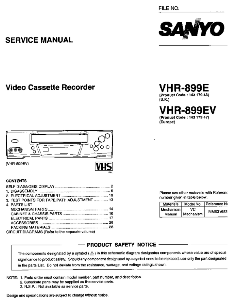
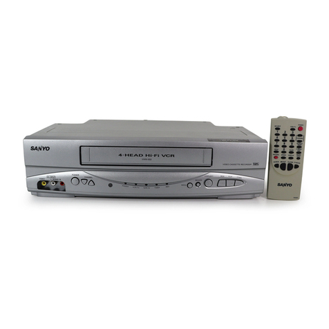
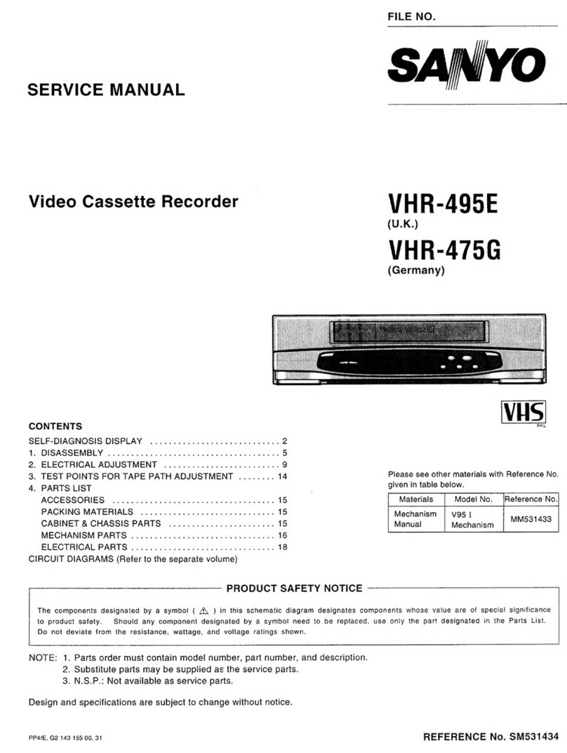
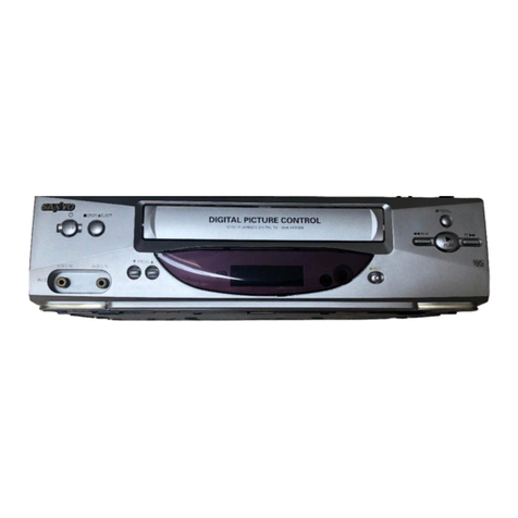
Sanyo VHR-420 User manual

FILE NO.
.+%,
..J
. . . ..
SERVICE MANUAL
Video Cassette Recorder VHR-420
(Australia and New Zealand)
ml PAL
CONTENTS
SELF-DIAGNOSIS DISPLAY ............................2
1.
2.
3.
‘e
,.
,. 4.
..
DISASSEMBLY. ............. .......................3
ELECTRICAL ADJUSTMENT .........................6 Please see other materials with Reference Nc
TEST POINT FOR TAPE PATH ADJUSTMENT .........13 given intablebelow.
PARTS LIST Materials Model No. Reference No
ACCESSORIES ...................................14
PACKING MATERIALS .............................14 P90
Mechanism WM-530599
CABINET &CHASS{S PARTS . . . . . . . . . . . . . . . . . . . . ...14 Mechanism
Manual
MECHANISMPARTS . . . . . . . . . . . . . . . . . . . . . . . . . . . . ...15 ’94MidiMid-
MountMechanism MS531346
ELECTRICAL PARTS ...............................18 III
CIRCUIT DIAGRAMS (Refer to the separate volume)
~“0’””“’’” ‘“”c’
The components designated by a symbol ( ~ ) in thisschematic diagram designates components whose value are of specialsignificance
tO product safety. Should any component designated by a symbol need to be replaced,use only the part designated in the Parts List.
DO not deviate from the resis!ence, wattage, and voltage ratingsshown.
k!~~~: ~. Fa~SOrd~r mUSt COnt~in mOde[nUrnber, part number, ar,ti6esciipliOn.
2. Substitute parts may resupplied asthe service parts.
3. N.S. P.: Notavailable as service park.
C
..
.
Design and specifications are su~j~ct to change without notice,
3
REFERENCE No. SM53142?

... . . ..... .
., .-
~1
PWMECHA(2)1/1
SELF-DIAGNOSIS DISPLAY
This unit displays the results of the self-diagnosis it carries out in two digits on the front panel indicator when problems occur.
Although these digits will only roughly tell you what kind of problems have occurred, use them when setwicing the unit. o
1, Displaying the Self-Diagnosis Results
●Press the STOP button for about 10 seconds continuously. Two digits (see below) showing the results of the self-diagnosis
will be displayed for three seconds at the hours part of the timer. All other parts of the timer will go off. The time will
automatically return after the three seconds.
●If no mechanism unit problems have occurred up to now, “00” will be displayed.
1
~Self-diagnosis digits
2, Self-Diagnosis Results
.,
No, Problem Main Possible Cause Mechanism Operations and
State After Occurrence
The cylinder motor does not rotate. ●-The cylinder motor is faulty. Shifts to the STOP mode.
01 ●The control of the cylinder motor is
faulty.
cThetapewindsaroundthe cylinder.
The take-up reel does not rotate. ‘
02 The take-up real is caught. Shifts to the STOP mode.
●The belt is faulty.
●The take-up torque has decreased.
The capstan motor does not rotate. ●The capstan motor is faulty.
03 Shifts to the STOP mode.
9The control of the capstan motor is
faulty.
The tape cannot be loaded with the “Error in the operations of the tape Unloads, shifts to the INITIAL mode,
cassette inserted. loading mechanism. and the power goes off.
(But unloading can be performed.) ‘
04 Foreign particles in the tape load-
ing mechanism.
●The tape end sensor is faulty.
●The reel brake of the tape cassette
has not been released.
Tape loading and unloading cannot be ●The tape guide is caught. The power isforcibly turned off with the
05 perrormed with the cassette insetied. “The loading motor is faulty. mechanism at its current position.
●The control of the loading motor is
faulty.
Front unloading cannot be performed “The cassette holder mechanism is Front loads and shifts to the STOP or
when ejecting the cassette. faulty. INITIAL mode.
(Front loading can be performed.) “The front door is caught. When the power switch is turned on
06 before eject operations:
Shifts to the STOP mode.
When the power switch is turned off
before eject operations:
Shifts to the INITIAL mode and
the power goes off.
Front loading and front unloading ●The tape cassette is caught in the The power isforcibly turned off with the
cannot be performad when ejecting cassette holder mechanism. mechanism at its current position.
07 the cassette. ●The gears of the front loading
drive mechanism have not en-
gaged properly.
The mechanism becomes 1(BRAKE) ‘The mechanism mode switch con- The power is forcibly turned off with
08 while moving from 2(STOP, FF/REIV), tact is faulty. the mechanism Et its current pcsi?ion.
3(ST[LL), 4(PLAY), and to 5(IDLER).
The mechanism becomes 7(INITIAL) ●The mechanism mode switch con- Carries cut tepe t~i:e-tip opei-elicns,
09 while moving from 1(BRAKE), 2(STOP, tact is faulty.
FF/REW), 3(STILL), 4(PLAY), and to 5shifts to the iNITIAL mode, and the
(IDLER). power goes off.
hlote: For details of mechanism operations corresponding to the mechanism positions of the self-diagnosis numbers 08 and ,,,,
09 above, refer to the separate volume on the mechanism manual. These manual reference numbers are s$iown in the ~
cove r. @
–2–
M1.14800(1)1,3
.
@
1. DISASSEMBLY
1-1.REMOVAL OF CABINET, MECHANISM UNIT AND MAIN BOARD
REMOVING THE CABINET PARTS(Fig.1.1.1) REMOVING THE CP-1 PWB ASSEMBLY (Fig. 1.1.3)
1. Remove the cabinet and bottom cover by removing the
four screws (A) and five screws (B). After removing the cabinet paits and mechanism unit:
2. Remove the front panel by removing the locks of the 1. Pull out the TM-1 PWB assembly while pressing and
clamps (C) using ascrewdriver, etc. and slightly rotating spreading outthefourclamps (l+) asshown bythearrows.
the bottom part in the direction of the arrow. 2. Remove the two red screws (J). Next, remove the CP-I
Note: Electrical adjustments for the this model can be per- PWB assembly by lifting it straight up while pressing and
formed with only the cabinet removed. spreading out the two clamps (K) as ahown by the
arrows.
REMOVING THE MECHANISM MAfN UNIT (Fig. 1,1.2)
After removing the cabinet parts
1. Remove the two screws (D), and then remove the bracket.
2. Remove the 22-wire flat cable from the MC-2 PWB, the 8-
wire flat cable from the VP-1 PWB assembly and the 6-pin
‘e
connector from the CP-1 PWB assembly resp~cfively,
3. Remove the mechanism main unit by removing the two
screws (E) and two screws (F).
Remove, as well, the two screws (G) at the cassette tray
side while pressing the tray lock lever as shown in the
enlarged view and pushing the cassette tray to the posi-
tion where the two screw (G) appear.
M-TK4/E-l (A)<ncabine’
Fig. 1.1.1
–3–

M1-14S01(N)23
M-TK2UE-2
Tray Look Lever able
Ca
Fig. 1.1.2
M-TK2UE-3
Mechanism M
Flat Cable
CP-1 PWB
TM
Clamps
Fig. 1.1.3
–4–
-.
e
@

M1-14801(1)~
TEMPORARILY SEITING UP AND CONNECTING MAIN PWB ASSEMBLY
m
e
;f,The following is an example of how to place and connect the main PWB not requiring ajig, when repairing the
CP-I PWB assembly (Fig. 1.1.4)
1. Place the mechanism main unit at the fixed position on 3. Place the CP-I PWB assembly above the mechanism
the chassis. main unit along the cassette holder. Insert the tip (L) of
2. Connect the 22-wire flat cable to the MC-2 PWB, and the the terminal board into the opening (M) at the side of the
8-wire flat cable to the VP-1 PWB assembly. chassis, as shown in the enlarge view.
●
M.TK2UE-4
CP-1 PWB Assembly
\TM-1 PWB
8-wire Flat Cable Terminal Board
w
1kICP-1 PWB Assembly
/
.....
I-Y’
Mechanism Main Unit’
‘e
Q
k..:
.y,w\y\Mc2pwB ..>,.,,..”,”.,
ACE Head “6-pin Connector
Opening (M)
Fig. 1.1.4
1-2. MAiN CIRCUIT BOARD
L-TEIUE
r
VP-1 PWB Assembly
Shield Case
(Power supply part)=
MC-2 PWB
(On the Mechanism Unit)
Tuner/lF/RF Conv. Unit
TM-I PWB~ _Cp.1 PWB
Fig. 1.2.1
–5–

S1-14S30(N) 1/2
2. ELECTRICALADJUSTMENT
2-1, SERVO CIRCUIT ADJUSTMENT
.These adjustments should be carried out upon completion of the tape transpofl adjustments.
.If the tape transpo~ adjustments (except the tilt adjustment) are carried out after these adjustments, follow the procedures
again in Section 2-1-3. SWITCHING POSITION ADJ.
.When acassette tape is loaded, auto-tracking will be set immediately after starting the first playback. AS thiswilldeviate the
tracking center set, be sure to press the channel buttons (+) or (-) once directly after starting playback to prevent auto-tracking
from being set.
2-1-1. TEST EQUIPMENT AND STANDARDS REQUIRED
Oscilloscope Vertical sensitivity: 5mV/DIV, external trigger
Band width: more than 10 MHz
Alignment Tape VHJ-0009 or VHJ-0023: SP mode, monoscope, 6KHz
Blank Tape VHS-type cassette tape
IMonitorlV I
2-1-2. LOCATION OF ADJUSTMENT POINTS
PlB243CKJB-Sl/2
[‘n uo0N*
~....
:..+.:
c) VR351
SW-P
!C251
L
o
................,
Q!
1: . . . .
POWER ~
SUPPLY ;
PART
IC301
Iclol :-...-:
Q
::
:...:
ICI 11
II .,,
,”7
“’F)‘E;* ‘fvn
?jTPlol VR103 vRi(
.........................Video Out CAR pB.\
VR201
—.. -........ I
BIAS !
[C*O1 u ‘[S!~c
TP202 ●~i
TP201 ●:~
(HOT) ;~
...
:.
:!
VR4flA .,
-+/w IC161 Q
.............
.....,-.--,,.---t,----1
~Tp103 :........... Tuner/lF/RF Conv. \ \
Unit
ft .........
)1
{
CP-I PWB (FOIL SIDE) Fig. 2.1.1
I
,
,
6“.,
–6–
.— -

SI.14B29(N) 2J2
P1B08800C.S1
Shield case
‘0 +
J~T ~
‘1
-. 0
-——
TP181
REC Current
TP183 SW-P VR182 REC-YIC
TP182 ENV
VP-1 PWB Assembly Fig. 2.1.2
Note:
●Self-recording means ‘Record any broadcasting or video
signal and play back the just-recorded portion=.
2-1-3. SWiTCH[NG POSITION ADJ.
Measuring Point Measuring Equipment ADJ. Condition
TPIOI Oscilloscope PLAY mode
(Video Out) Alignment tape
TP183 (SW-P) (VHJ-0009 or
VHJ-0023)
ADJ. Location AIM. Value
VR351 (SW-P) 6.5 HkO.5 H
1. Set the tracking control position to the center by pressing
CHANNEL buttons (+) and (-) simultaneously.
(Tracking center position display in the indicator
panel “T -:- ‘)
2. Adjust VR351 (SW-P) so that the width of ‘T” becomes
6.5 Hf0,5 Has shown in Fig. 2.1.3.
WS.SWP
T= 6,5 Hf0.5 H
Iverticalsync signal
+t
Rise RF. SW. PULSE
Fig. 2.1.3
2-1-4. STILL V-LOCK ADJ.
]Measuring Point IMeasuring Equipment IADJ. Condition I
Picture of Color bar generator Self-recording
monitor TV or STILL mode
Broadcasting Blank tape
Monitor
IADJ. Location IADJ. Value I
CHANNEL (+) button The minimum vertical shake
CHANNEL (-) button
1. Play back the just-recorded portion and then set the VCR
in the STILL mode.
2. Press the CHANNEL(+) button orthe CHANNEL(-) button
so that any vertical shake of the picture is brought to its
minimum.
–7–

v1-14s01(N)1/4
2-2. VIDEO CIRCUIT ADJUSTMENT
.Before making the following adjustments, Section 2-1. SERVO CIRCLJiTADJUSTMENT should be completed.
.Use the relay jig to provide simple adjustment of the VP-1 PWB assembly.
2-2-1. TEST EQUIPMENT AND STANDARDS REQUIRED
Color Bar Signal Generator PAL Color barsignel with 100% white level (EBU color barsignel)
Oscilloscope Vertical sensitivity: 5mV/DIV, external trigger
Band width: more than 10 MHz
Digital Voltmeter DC range
Alignment Tape VHJ-0008 or VHJ-0023: SP mode, color bar, lkHz
(Color bar signal waveform is described below. Refer to Fig. 2.2.1)
Blank Tape VHS-type cassette tape
Oscilloscope Probe Input capacity less than 25 pF (10:1)
Iessthan 40 pF (1:1)
Covering frequency: DC -40 MHz (10:1)
DC-30 MHZ(1:1)
Frequency Counter 8significant digits
Adjustment Relay Jig VHJ-0065: 5-wire flat cable for VP-1 PWB Assembly
ALIGNMENT TAPE COLOR BAR SIGNAL
‘H.Sync Sl&al
COLOR BAR SIGNAL WAVEFORM (VHJ-0008)
Fig. 2.2.1
W W-TCP
m
m
gs z
co
COgg
3:~6;g:
(75%)
Yu Iw?fe
White Black
COLOR BAR PAITERN (VHJ-0008) ON MONITOR TV
Fig. 2.2.2
2-2-2. ADJUSTMENT RELAY JIG
Connect the flat cable end from the cylinder assembly to the
VP-1 PWB assembly using the relay jig to provide simple
repairing and adjustment of the VP-1 PWB assembly, as
shown in Fig. 2.2.3. Further, when adjusting the VP-1 PWB
assembly, be sure to make contact an end of shield case with
bracket of the VP-1 PWB assembly to maintain the shield
effect. If the VP-1 PWB assembly does not contact, there is
insut%cient ground and no proper play back image can be
obtained.
WPV-TK2UE VP- IPwn
*’
uAssemb
Bracket
Relay Jig ‘m
(VHJ-0065) “
\
o
Flat Cable ~! \
,, I
Ifs’
L4
“’:’’y-fel%?
““
Ily
Fig. 2.2.3
–8–

@
VI.14B30(1) 2’4
2-2-3.LOCATION OF ADJUSTMENT POINTS
PlBo8803c-vl
Shield Case
o
‘1”
+
A)T
-- 0
———
TP181
REC current
TP183 SW-P VR182 REC-Y/C
TP182 ENV
VP-1 PWB Assembly Fig.2.2.4
PIB24303B-Vl/2
“o
uF
o0
.
‘,.. (F (;;.!
:....
...,.’
(3
VR351
...
IC602 o
SW-P
IC351
IC301
o... ..............
Q[ VR201
i... IC201 c1
BIAS [------~
/...
:e: :~
,....’ :
TP202 ●\ !
POWER ~
SUPPLY ;~-:
,:
PART ]VR104
IC162 VR102 DEV
oAGC
4/0 --!cj.6j.-, a
,--..:;---;;-.-/:--;
,TP103 ‘.--. ”--”-.-’
v
Unit
TP1020~.?.c7 .$.; 0.........
!TPIOI VR103 VR101
:.......................! Video Out CAR PB-Y
CP-I PWB (FOIL SIDE) Fig.2.2.5
Icl 01 ~“’.~
c)
:...:
Iclll

V1.14B29(N) 3/4
Notes:
●Connect the monitor TV to the VIDEO OUTPUT terminal,
before making following adjustments.
.Self-recording means ‘Record the video signal and play
back the just-recorded portion”.
2-2-4. AGC LEVEL ADJ.
~
Measuring Point Measuring Equipment ADJ, Condition
IADJ. Location IADJ. Value
VRI02 (AGC) 0.5 Vp-p k0.025 VP-p
1. Connect the color bar generator to the VIDEO INPUT
terminal.
2. Adjust VR102 (AGC) for 0.5 VP-P f0.025 VP-P as shown
in Fig. 2.2.6.
WPV-AGC 100% \Vhite
L4
0.5 VP-p *0.025 Vp-P
Lr
, ,
Fig. 2.2.6 1
2-2-5. PB-Y LEVEL ADJ.
Measuring Point Measuring Equipment ADJ. Condition
TP101 Oscilloscope PIAY mode
(Video Out) (10:1 probe) Alignment tape
(VHJ-0008 or
VHJ-0023)
AlXl. Location ADJ. Value
VRIO1 (PB-Y) 1Vp-p *0.05 Vp-p
1. Terminate the VIDEO OUTPUT terminal with a75!2
resistor.
2. Adjust VRIO1 (PB-Y) for the video iuminance si9nal level
Of 1vp-pt 0.05 VP-P. (Refer to Fig. 2.2.7)
WPV.PBY White
1Vp-p *
2-2-6. CARRIER SET ADJ.
Measuring Point Measuring Equipment ADJ, Condition
TPI03 \Color bar generator IREC mode I
Frequency counter
IJ
ADJ. Location IADJ. Value I
VRI03 (CAR) 3.83 MHz *0.05 MHz I@
.,
.,.
1. Connect the color bar generator to the VIDEO INPUT
terminal.
2, After removing the first color bar signal input from the
video input terminal, immediately adjust VR103 (CAR) so
that the frequency becomes 3.83 MHz +0.05 MHz.
2-2-7. DEVIATION ADJ.
~
Measuring Point Measuring Equipment ADJ. Condition
II
IADJ. Location ADJ, Value i
1
VRI04 (DEV) 1Vp-p i0.05 Vp-p
1. Record the color bar signal on the blank tape. e
2. Play back the just-recorded portion.
3. Adjust VRI04 (DEV) for 1Vp-p t0.05 Vp-p as shown in
Fig. 2.2.8.
4. If the adjustment value is not satisfactory, adjust VR104
(DEV) and repeat steps 2to 3.
WPV-DEV ..... .... .
~Y-lH+”
Fig. 2.2.8
–1 o–

.
VI-14829(NI 44
t2-2-8.Y/C REC CURRENT ADJ.
0,
d
Measuring Point Measuring Equipment
●
.
TP181 Color bar generator
(on VP-1 PWB) Oscilloscope
(1:1 probe)
ADJ. Condition
REC mode
Blank tape
ADJ. Location AW. Value
VR182 (REC-Y/C) 650 mVp-p *20 mVp-p
1. Connect the ground of the oscilloscope to the shield case
of the VP-1 PWB assembly.
2. Adjust VR182 (REC-Y/C) so that the video luminance
signal level at the sync tip is 650 mVpp t20 mVp-p.
(Refer to Fig. 2.2.9)
IWV-YREC
650 mVp-p
ISync Tip
IFig.2.2.9
–11-

A1-14801(1)1/1
2-3, AUDIO CIRCUIT ADJUSTMENT
e
.
.Before making these adjustments, (especially, the tape ●Before making these adjustments, Section 2.1. sERVO
guide height and audio control erase head height adjust- and Section 2-2. VIDEO circuit adjustments should be
ments) should be carried out, so that the tape traveling carried out.
between the loading guide pole and the audio control
erase head runs without fluttering, twisting, curling.
2-3-1. TEST EQUIPMENT AND STANDARDS REQUIRED
Oscilloscope Vertical sensitivity :10 mV/DIV
Band width :more than 30 MHz
AC Voltmeter Effective value indication
Input frequency :lOHz-20kHz
Input Impedance :more than 1‘MQ
Measurement level :1 mV (full scale)
Blank Tape VHS-type cassette tape
2-3-2. LOCATION OF ADJUSTMENT POINTS -
P1B24300B-AV3
oC)v
~...,
:e:
.....
c1 VR351
SW-P
IC351
IC161
.............
.............
CP-1 PViB (FOIL SIDE) Fig. 2.3.1
2-3-3. BIAS LEVEL ADJ.
@
,., ,
Measuring Point Measuring Equipment ADJ. Condition
TP201 (HOT) Oscilloscope REC mode
TP202 (COLD) AC voltmeter Blank tape
I
ADJ, Location ADJ. Value
VR201 (BIAS) 26 mVrms
1. Load the VCR with ablank tape and select the record
mode without all incoming signal.
2. Af%rccnt3r~, ingon the csc;l!csc~c~ ‘h=ta 70kHz+5 W!z ‘
k,. ”.,.-
sine wave is being output, adjust VR201 (BIAS) so that
the AC voltmeter’s reading is 26 mVrms.
—’12–

T-TLl/A2(N)W
2-4. TUNER AND IF CIRCUITS ADJUSTMENT
●When any malfunction occurs in the TUNER circuit the Note:
whole unit must be replaced.
.An adjustment of the IF circuit is shown as follows.
2-4-1. TEST EQUIPMENT AND STANDARD REQUIRED
The TUNER unit does not need any adjustments,
because precise adjustments have been performed
before shipment.
,“
e
---
IMonitor TV II
2-4-2.LOCATiON OF ADJUSTMENT POINT
PPFUSO030-R1
(_
o
Tuner/lF/RF ~(
Conv. Unit
~
t
J
VR (RF AGC)
IF UNIT(PARTS SIDE)
Rear Panel
CP-I PWB
Fig. 2.4.1
2-4-3. RF AGC ADJ.
Measuring Point Measuring Equipment ADJ. Condition
Picture of Monitor TV E-E mode
monitor TV
ADJ. Location ADJ. Value
VR (RF AGC) SIN is best point
(onthe IF circuit)
1.
2.
3.
4.
Connect the monitor TV to VHF/UHF ANTENNA OUTPUT
terminal.
Connect the VHF antenna to VHFLJHF ANTENNA INPUT
terminal.
Receive the middle electrical field (70 dB# -90 dBp) of the
VHF high channel, and slowly turn VR (RF AGC) from the
point where snow-noise is present to the point where it
just disappears from the monitor TV.
Confirm bymonitor TVthatthere isnobeatandsatu ration
3. TE~ POINT FOR TAPE PATHADJUSTMENT
(S/N is bestpoint) when receiving any TV channel.
Test point TP182 (ENV) and TP183 (SW-P) for tape path adjustment is shown in Figure below.
For adjustment, refer to the Mechanism Service Technical lnformation(WM-530599 and MS531346).
)—Shield Case
t
(~
0/7’(”
U@)
.- 0
———
TP181 REC Current
P1B08800C-T3
VP-1 PWB Assembly Fig.3.1
II
–13–
.

4. PARTS LIST
LOCATION PARTS NO. DESCRIPTION
ACCESSORIES
645004 8333 REMOCON(WITH COVER BATTERY)
613 147 3591 COUER BATTERY(FOR REMOCON)
613 155 3743 INSTRUCTION tlCiNUOL
613 096 6773 CAEiLE,ANT
OR 613011 7359 ~:~~
OR 613 132 6132 CA3LE,ANT
OR 613 132 5975 CORO
A645002 7642 CORD,POWER
%*********%****x*************%******%**************************
PACKINGMATERIALS
613 155 4108 CARTON CASE
613 1502277 CUSHIONrFRONT
613 1502284 CUSHION,BACK
613099 1768 POLYE COVER,INNER-K
LOCATION PARTS NO.
CABINET&CHASSISPARTS
CH-1 411 1370007
CH-2 411 021 7907
CH-3 411 001 1901
CH-4 613 1542754
CH-5 4120289406
CH-6 613 1407015
CH-7 411 021 3800
CH-8 613 1537859
CH-10 613 1553811
CH-11 6450029608
CH-12 613 1392182
CH-13 613 1450707
CH-14 613,121 1001
CH-15 613 1532465
CH-16 613 1554054
CH-17 613 1407459
CH-18 613 1563346
DESCRIPTION
SCR L-TPG BIN 3X1O
SCR S-TPG BIN 4X12
SCR S-TPG BIN 3X6
COMPL PWB,UP-1
SPECIAL SCREW
COVER TOP
SCR S-TPG BIN 3X1O
TERMINAL
COMPL PWB,CP-1-A
TUNER,RF/TU/IF
COVER BOTTOM
STANO,BACK
STANO,FELT.FRONT
COMPL PWB,Tfl-1
DOOR CASSETTE
SPRING
ASSY,CABINET FRONT
7
8e

MECHANISM PARTS
LOCATION PARTS NO.
MECHANISMPARTS1
CD-1
co-4
CD-5
CD-6
co-7
CD-8
co-9
CD-10
CD-11
CO-12
CD-13
CD-14
CO-15
CO-16
CO-17
CO-18
CO-19
CD-20
CD-21
CD-22
CO-24
CO-27
CD-28
CD-31
HA-1
MA-2
MA-3
MA-4
MA-5
MA-6
OR
HA-7
OR
613 142 9581
6130220585
407 0983201
411 0159801
613022 1643
613022 0073
6130222695
613 141 6109
613 1398962
613 022 2626
613021 9657
411 027 1305
6130950949
411 1069208
6130220943
6130222619
613 022 1667
613022 2596
6130220097
613022 1674
613022 4064
613 124 5006
613 1256149
411 001 8702
613 1000391
6130857996
613021 9701
411 144 2803
411 109 1605
613 1357068
613 135 7S49
613 1357075
613 1432963
DESCRIPTION
COMPL,CASSETTE MECHANISM
LID
PHDTO COUPLE PN150S!AN
RING E 2.3
SPRING,LINK L
ASSY,GEAR,LEUER L
RACK
GEfJR,LOCK
ASSY,LEVER,PINION
GEAR,PINION
ASSY,BRACKET,GEAR
SCR S-TPG BIN 2.6X4
SW,SPECIAL
SCR PAN+SW+W 2X9
HOLDER,TRANSISTOR
GEAR,IDLER
SPRING,GEAR MAIN
GEAR,MRIN
ASSY,GEAR,LEUER R
SPRING,LINK R
BOORD,UNOER
LEUER,SOFETY SW
SPRING,SRFETY SW
SCR BIN 3X6
ASSY,LEUER,TENSIDN
SPRING,LEUER TENSION
ASSY,HOLDER,BAND
SCR PAN+SW+W 2.6X6
WASHER Y 2.6X6X0.25
ASSY,REEL,SUPPLY
ASSY,REEL,SUPPLY
ASSY,REEL,TAKE UP
ASSY,REEL,TAKE UP
LOCATION
MA-8
OR
OR
MA-9
OR
MA-10
OR
MA-11
MA-12
OR
MA-15
MA-16
MA-17
MA-18
MA-19
MA-20
MA-21
MA-22
MA-23
MA-24
MA-25
MA-26
MA-27
MA-28
MA-29
MA-30
MA-31
MA-32
MA-33
MA-34
MA-35
MA-36
MA-37
MA-38
MA-39
PARTS NO.
412 021 5306
412 015 8900
412015 8504
411 109 1506
411 109 1407
613 1357150
613 142 9116
412026 7305
613 1357167
613 142 9109
412 042 4302
613 135 7099
411 120 1301
613 1357082
411 021 3107
613 1209053
4070167205
613021 9985
613 1429086
613022 1612
613022 1506
613098 0106
6130773647
613022 1490
6130222374
613084 8871
6130220004
6130809216
6130862914
6130809209
411 1093005
6130222015
412015 9501
411 021 7907
412045 4606
CB602700
DESCRIPTION MBO05 1:*
SPECIAL WASHER 3.1X6X0.3
SPECIAL WASHER 3.1X6X0.4
SPECIAL WASHER 3.IX6X0.5
WASHER Y 2.1X6X0.25
WGSHER Y 2.1X5X0.25
GEAR,REEL SUPPLY
GEAR,REEL SUPPLY
SPECIAL WASHER 2.6X6X0.25
GEAR,REEL TAKE UP
GEAR,REEL TAKE UP
SPECIAL SCREW 2.6X4
COMPL,IOLER,CLUTCH
WASHER Y 2.1X4X0.25
ASSY>IDLER
SCR S-TPG BIN 2.6X8
COMPL PCB,MC-4
LED LN59
ASSY,SLIOE,ACT PLATE
SLIOE,C BRAKE
SPRING,RETURN SLIOE
SPRING,SUB T
ASSY,BRAKE SUB T
PULLEY,REEL
SPRING,SUB SUPPLY
SLIOE,ACT BRAKE
BRAKE,SUB SUPPLY
ASSY,SLIOE,M PLATE
ASSY,BRAKE,SUPPLY
SPRING,tiAINBRAKE
ASSY,BRAKE,TAKE UP
WASHER Y 2.6X5X0.5
LEUER,CONT PLATE
SPECIAL WASHER
SCR S-TPG BIN 4X12
SPECIAL WASHER 2.4X6X0.25
Undesignated numeral shows
CD-1 9+-CD-31 Location No.:MA- 9---15
–15–

DB806800
LOCATION PARTS NO.
MECHANISMPARTS2
OR-1
OR
OR
OR
OR-2
OR-3
OR
OR-4
OR
OR
OR
OR-5
OR-6
OR
OR-7
OR-8
OR
OR-9
OR
OR-10
OR
OR
OR-11
OR-12
OR
MB-1
MB-2
MB-3
MB-4
MB-5
MB-6
f4B-7
MB-8
MB-9
HB-iO
MB-11
MB-12
MB-13
MB-14
MB-15
MB-16
MB-17
MB-18
MB-19
MB-20
MB-21
MB-22
MB-23
MB-24
OR
MB-28
MB-29
MB-30
MB-31
tlB-32
MB-33
MB-34
t’iB-35
KB-36
MB-37
MB-58
MB-39
tlB-40
tlB-41
hiB-42
MB-43
613 1429567
613 1320468
613 114 2800
613 114 2794
411 038 1608
613 1142831
613 1142824
613 1086241
613 113 1354
6130772138
6130220271
6130972170
6130221001
6130889072
411 047 7509
4120309708
411 0475000
6130857279
613 1323520
4120360709
411 044 8301
411 044 9209
6130224019
412036 0808
411 o~4 ?001
613 1234802
6130533227
613 1234970
411 004 5302
613 1239418
613 152 8079
613021 9800
411 10? 2GJE
613 022 1797
bii i++ 579’1
613 110 1692
412015 8207
411 1200007
613 1203631
613022 1582
613094 9240
613022 1575
6130222725
6130222534
613094 1206
613 134 2910
411 0468002
411 0232801
411 0233303
411 021 3107
613077 3227
6130270382
6130788320
613 117 0599
6130939159
6130938374
613077 3616
613 121 9960
613092 9945
6?3 152 F075
613 ‘!535107
613 ilo 0374
411 126 5303
613 092 9921
613 092 5?85
613092 59?2
DESCRIPTION LOCATION PARTS NO.
COMPL,CYLINDER,2N2S-V
COMPL,CYLINDER,2N2S-U
SCR PAN+W 3X8
ASSY,CYLINDER,UPR 2N2S-U
ASSY,CYLINDER,LWR 2AL
ASSY,CYLINDER,LWR 2
ASSY,CYLINDER,LWR 2
SPACER,MOTOR O.3T
BASE,CYLINDER
BASE,CYLINDER
SCR PAN+FLG 3X6
SPECIAL SCREW 2.6X8
SCR PAN+FLG 2.6X8
STATOR,MOTOR CYLINDER
SPECIAL SCREW 2.3X1O
SCR PAN+SW 2.3X1O
SCR PAN+SW 2.3X8
ROTOR,MOTOR CYLINDER
SPECIAL SCREW 2.3X6
SCR PAN+SW 2.3X6
SLEEVE
SPECIAL WASHER
TAPE GUIDE
NUT HEX (3)
CAP
SLiDE.ACT PINCH
ASSY,LEUER,CAM PING-!
Wl%w Y 3.ix&xo.5
SPRING,!2CEHEAD
(Ai+L .bkfi~~i~ ,nEA2
SLEEVE,ACE HEAD
SPECIAL NUT (MS)
SCR PAN+SW+W 2.6X5
BRACKET,STOPPER
SPRING,SLIDE BRAKE
COMPL.SLIDE,CAtl
SPRING,LINK LOCK
DAMPER
GEAR,FRONT LOAD
PSSY,LEVER,FRONT
GEAR,HELICAL FRONT
SCR PAN+SW+W 2.6X6
SCR S-TPG PAN 2.6X6
SCR S-TPG PAN 2.6X8
SCR S-TPG BIN 2.6X8
HOLOER,WORM
WASHER
ASSY,WORM,FRONT
BRACKET,HOLOER
PLATE}NUT
DAMPER,MOTOR
DAMPER,WORM
ASSY,LOADING HOTOR
OAkiPER,t’IOTOR
COHPL PC9,Yt-3
COtiPLPWB,MC-2
ROTARY SWITCH
SCR PbN 2.(Y’!3
ASSY,SLIOE,FROfT
SPRi!4Ci.LEVER LGA3
SPRi!{3,LZUER ;CT
MB-44 6130925886
OR 613 1388628
MB-45 6130270627
flB-46 6130929938
MB-47 6130222985
MB-48 4120334106
MB-49 6130773579
MB-50 613 1029293
MB-51 613022 1568
MB-52 6130220158
MB-53 613 1479951
tlB-54 411 1092107
MB-55 6130788160
MB-57 613 1357655
MB-58 613 1455009
MB-59 6131455016
MB-60 411 0630904
MB-61 6130220233
MB-63 6450002533
MB-66 613 153 1871
MB-67 613022 1698
MB-90 613 1538627
DESCRIPTION MBoo51##
HOLDER,WORM e
HOLOER,WORM
WASHER 2.1X6X0.5
ASSY,WORM,LOAD
BELT,LOADING
WASHER SLIT 2.6X5X0.50
GEARtHELICAL
ASSY,LEVERrREV GUIDE
SPRING,REVIEW LEVER
COMPL,PINCH ROLLER
SPRING,PINCH ROLLER
WASHER Y 3.6X6X0.5
COMPL,LEVER,ACT BRAKE
PLATE,BGR
ASSY,MOUNTING,ROLLER
SCR SET HEX-SCT 2X3
ASSY,GUIDE,ROLLER
HEAD,FULL ERASE
LEVER,FE HEAD
SPRING,ERASE HEAD
s
T
FLEXIBLE FLAT CABLE,CN811-CN303 _
MECHANISMPARTS3
Ilc-1
MC-2
MC-3
MC-6
MC-7
MC-8
MC-9
MC-10
MC-12
MC-13
MC-14
MC-15
MC-16
MC-17
MC-18
MC-19
MC-20
MC-22
MC-23
MC-24
MC-25
MC-26
MC-27
MC-28
MC-29
MC-30
MC-31
HC-34
MC-35
MC-36
MC-37
MC-38
MC-40
nc-41
-16–
6450005053
6130222978
613 155 4609
613022 1520
6130823434
613022 1711
613081 7518
6130982285
411 021 3107
411 1P? 2008
613 142 9093
6130222701
411 109 1902
613 1357666
613 1357532
411 109 1803
613 1357648
411 047 6809
613021 9763
613 1357662
613 022 1551
613021 9879
6130906373
613022 1704
613021 9862
6130222039
613091 3104
411 0286309
4120158603
613 1309890
4120454606
411 0920906
411 1000300
613 1209060
MOTOR,CAPSTAN OC 3W
BELT,REEL ORIVE
COMPL.LEVER,CLUTCH
SPRING,LEVER CLUTCH
LEVERtCHANGE CLUTCH
SPRINGtCHANGE CLUTCH
ASSY,BRAKE CAPSTAN
SPRING,CAPSTAN
SCR S-TPG BIN 2.6X8
WASHER Y 3.lXtX:.5
SLIi)ErCAM PLATE
CAM,MOOE
WASHER Y 3.1X6X0.5
CAM,MAIN
ASSY,RACK,LOAO
WASHER Y 2.6X6X0.5
SPACER,RACK LOAD
SCR PAN+FLG 3X4
ASSY,EARTH,CYL
GEAR,LoAo TAKE up
SPRING,GEAR LOAO T
ASSY,LEVER,LOAO T
GEAR,LOAO S
SPRING,GEAR LOAD S
ASSY,LEVER,LOAO S
LEVER,RETURN TENSION
ASSY,LEVER CONTROL
SCR S-TPG PAN 2.6X6
SPECIAL WASHER 3.1X6X0.25
ASSY,GEAR,FRICTION
SPECIAL WASHER 2.4X6X0.25
WASHER Z 2.6X1OXO.5
SCR S-TPG BIN 2.6X5
COMPL,MC-1

MECHANISM PARTS 2 Undesignated numeral shows
‘-,, Location No.:MB-
,//Q:DR:2----- ‘,,, y “+? zf ‘fl>;
1!
e61
58
6
.
‘,
-J
i‘+
Q
+7
966
.10 ,
I
11+,
M
10+
-----
‘+@ 63
3$
3+
‘+.0 @-’’bQ)
&+ DR-12 ‘-l
/1
FiEEEl””
MECHANISM PARTS 3
ta p,+...:.... .;,
L.s...-dz.-.-d:.:irieralshov;s
Location No.:MC- W
12+ -
ml
2--
41
EIEizIE N.S.P.:Not available as service parts
–17–

ELECTRICAL PARTS
NOTE;
1,
2.
3.
4,
5.
6.
Materialsof Capacitorsand Resmtors aresbbrevlated as follows;
Resistors TA-SOLID Tantalum SolidCapacitor
MT-FILM MetallizedFilm Resistor AL-SOLID Aluminum SolidCapacitor
MT-GLAZE MetallizedGlaze Resistor NP-ELECT Non-Polarized Electrolytic
OXIDE-MT Oxide MetallizedFilm Resistor Capacitor
OS-SOLID Aluminum SolidCapacitor with
Caqaz’lors OrGanic Semiconductive
MT-POLYES MetallizedPolyesterCapacitor ElectrolyticCapacitor
MT-COMPO MetallizedComposite Capacitor DL-ELECT Double Layered Electrolytic
Capacitor
Tolerance of Capacitor(lOPF over)and Resistorarenoted with followsymboles.
F............~~y~ G............~pf~ J.,..........=~o~o K............+l OO/O
M.,..........*2@jo N............& 3@/o z . . . . . . . . . . ..+eoo~ -–2Qo/o
Capacitors
U:UF P:PF
Inductors
UH : UH MH : mH
N.S.P. :Not availableas serviceparts.
The ceramic capacitorssnd resistorsmounted on thePWB,may be two differenttypesofparts,chip(leadleas)typeordiscrete(withIesd
wire)type.Therefore,eventhough the locationnumber isthe &me,you may encounter either chip or diswete partson the PWB.
LOCATION PARTS NO.
CdiPL PHB,CP-I-A
COf4PL.NO 613 155 3611
(SEHICGWJCT6RS)
Q1002
0?
0?
CR
G1OO3
OR
OR
OR
Q1OO4
OR
(N
OR
Q1OO6
OR
OR
OR
Q1011
OR
Q1012
OR
OR
OR
Q1151
OR
Q1152
OR
Q1601
OR
Q2001
OR
OR
C2002
0?
Q2003
Oi
405 057 6201
405057 6409
405 123 7002
LOS 123 7101
405 064 0100
405 064 0209
405 1236708
405 123 6807
405 064 0100
~05 064 0209
405 123 6708
405 123 6807
405057 6201
405 057 6409
405 123 7002
405 123 7101
4050639708
405 123 6500
405 057 6201
405 057 6409
405 123 7002
405 123 7101
4050639906
405 123 6401
405 063 9609
405 124 2709
405004 4601
405 006 1806
405 0180002
405 018 0101
405 018 0200
405 063 9708
405 123 6500
405 003 7702
405 000 1208
405 063 ?708
.705123 6500
Lfj5135762(II
DESCRIPTION
TR 2SC4038-Q
TR 2SC4038-R
TR 2SD1991A-Q
TR 2SD1991A-R
TR 2SA1561-Q
TR 2SA1561-R
TR 2SB1320A-Q
TR 2SB1320A-R
TR 2SA1561-Q
TR 2SA1561-R
TR 2SB1320A-Q
TR 2SB1320A-R
TR 2SC4038-Q
TR 2SC4038-R
TR 2S01991A-Q
TR 2S01991A-R
TR DTC144EL
TR UN6213
TR 2SC4038-Q
TR 2SC4038-R
TR 2S01991A-Q
TR 2S01991A-R
TR 0TC124EL
TR UN6212
TR 0TA114EL
TR UN6111
TR 2SA608-F-SPA
TR 2SA933S-R
TR 2SC3331-S
TR 2SC3331-T
TR 2SC3331-U
‘iR0TC144EL
TR UN6213
TR 2SA15L6
TR DTA124ES
LOC4TION
Q3553
OR
OR
Q5001
OR
Q5002
OR
Q5003
OR
Q5004
OR
Q51~l
OR
Q5102
OR
Q5103
OR
Q5104
OR
Q6001
OR
OR
OR
OR
OR
OR
Q6002
OR
Q6601
OR
Q6901
OR
OR
OR
OR
Q6902
OR
OR
OR
OR
Q6903
OR
PARTS ND.
405 057 6409
405 1237002
405 123 7101
405 094 6905
405 1260208
405 013 7096
405 cl;?73f)3
405 006 6702
4050067204
4050137006
405 013 7303
‘LP5015 7023
405 0137303
405 015 7006
405013 7303
4050037603
4050002205
4050182501
4050006104
4050736407
4050736506
4050269004
4050269103
405 114 7806
405 114 7905
405 114 8001
4050182501
4050006104
4050182501
4050006104
405 019 2005
405 011 8401
4050930607
4050192807
405011 8500
405004 4007
405 006 1707
4050930508
405004 4601
405 006 1806
4050192005
405011 8401
DESCRIPTION
TR 2SC4038-R
TR 2S01991A-Q
TR 2S01991A-R
TR 2SK1460
TR 2SK1460LS
TR 2SC2274-F
TR 2SC2274K-F
TR 2SA984-F
TR 2SA984K-F
TR 2SC2274-F
TR 2SC2274K-F
TR 2SC2274-F
TR 2SC2274K-F
TR 2SC2274-F
TR 2SC2274K-F
TR 2SA1345
TR 0TA144ES
TR 2SC3399
TR 0TC144ES
TR 2SK772-E
TR 2SK772-F
TR 2SK222-O
TR 2SK222-E
TR 2SK1104-P
TR 2SK1104-Q
TR 2SK1104-R
TR 2SC3399
TR 0TC144ES
TR 2SC3399
TR 0TC144ES
TR 2SC536-E-SPA
TR 2SC1740S-Q
TR KSC2785-Y
TR 2SC536-F-SPA
TR 2SC17LOS-R
TR 2SA608-E-SPA
TR 2SA933S-Q
TR KSQ1175-Y
TR 2SA608-F-SPA
TR 2SA933S-R
TR 2SC536-E-SPA
TR 2SC1740S-Q
C
,:.
.
*,,
.,
@
@ii i
.
–18–

LOCATION F(%!TSNO.
Q6903 405 093 0607
OR 405 019 2807
OR 405 011 8500
Q6904 405 018 2501
OR 405 000 6!04
Q6921 405 084 8209
OR 405084 8308
(INTEGRATEDCIRCUITS)
IC101
OR
Iclll
IC161
OR
IC201
IC301
IC302
IC303
OR
IC351
OR
Icsll
IC512
IC602
OR
OR
OR
OR
OR
OR
OR
IC6?1
IC692
OR
(DIGDES)
D1OO3
OR
01006
OR
01007
OR
D1OO8
OR
DIO09
OR
01601
OR
01602
OR
D1611
OR
D3001
OR
03121
OR
03122
OR
D3123
OR
D3502 -
OR
4093260204
409 333 9900
409297 6205
4090034501
409 1203401
4092622409
410 216 1102
4093142005
4093130903
4092434101
409 3233109
4093486307
409067 7203
409225 2309
410 1773801
409 348 3702
410 1895602
410 1726708
410 1773603
4093486802
410 1895701
410 1726807
4090196209
409 026 8203
409057 5103
407 0079904
4070124406
4070079904
4070124406
407007 9904
4070124406
4070079904
4070124406
407 0079904
407 0124406
4070079904
407 0124406
407007 9904
4070124406
407 0707104
4070536704
407 0124406
407 007 9904
407 012 4406
407 007 9904
407 012 4406
407 007 9?04
407 012 4406
407007 9904
407 007 9904
4070124406
DESCRIPTION LOCATION
TR KSC2785-Y
TR 2SC536-F-SFfl
TR 2SC1740S-R
TR 2SC3399
TR DTC144ES
TR 2SC2960-F-S?A
TR 2SC2?60-S-S?A
IC LA7345AM
IC Lf+7345M1-tiPB
IC LC89925
iC L?A7021
IC Lf+7221
IC LA7285M
IC LC866636V-5584
IC LB1643
IC MN1381-L
IC HN1380-L
~c ~L12806K
IC XLU2896K
IC L5431
Ic PQ12RF11
IC AT24CO1A-1OPC
IC XL24C01AP
IC 24LCOlB/P
IC X24C01AP-C7284
IC AT24C02-IOPC
IC XL24C02P
IC 24LC02B/P
IC X24C02P-C7189
IC Lt$79i0
IC L565i
IC UPC574J
DIODE G1’If+Ol
OIOOE 1SS133
OIOOE G!MO1
OIOOE 1SS133
OIOOE GY401
OIOOE 1SS133
OIODE GMAOI
DIODE 1SS133
DIODE GMAO1
DIOOE 1SS133
DIODE GMOO1
OIODE 1SS133
DIODE GMAO1
OIOOE 1SS133
ZENER DIOOE GZS5.6X
ZENER DIODE MTZ5.6B
OIOOE 1ss133
OIODE &’AOl
OIOCIE1SS133
OIOCIEGtlAOl
OIODE 1SS133
OIODE GMAO1
DIOOE 1SS135
OIODE GMAOl
DIOOE G1’tAOi
OIODE 1ss133
D35i0
OR
05001
05003
05004
05006
05010
05013 A
05101
D5102
D5103
D5104
D5105
D5108
05109
05110
OR
05112
06901
OR
06902
OR
D6903
OR
PARTS NO.
407 007 9904
407 0124406
407 134 8900
4070782705
407 078 2705
4070782705
407 091 6704
407 151 3308
407 1695806
407 1695707
407 0782705
407 0782705
407 1006909
4070638903
407 0638903
4070049709
407 0058701
407 0638903
4070124406
4070079904
4070124406
407007 9904
4070124406
407 007 9904
(CRYSTALDEVICES)
Xlool 6450006012
OR 645 0006029
OR 6450024436
x3001 6450035852
OR 6450034510
X3002 645004 1938
OR 645004 1945
(VARIABLERESISTi3RS)
VR101 6450035265
OR 6450035456
VR102 /)450035258
OR 6450035449
VR103 613 1477223
OR 6450035388
VR104 6450035197
OR 6450020919
VR201 645001 8787
OR 6450035548
VR351 6450035166
OR 6450035593
(INDUCT6RS)
L1OO4 645 003 7979
OR 6450038327
L1OO5 6450037979
OR 645003 8327
L1OO7 645 0037993
OR 6450038334
L1OO8 645003 7?62
OR 645 001 6635
L101O 6450038068
OR 6450038426
L1OI2 6450038129
OR 645001 5496
L1013 6450038112
OR 645001 5489
L1081 6450037924
D~sc~Ip~IoN
DIODE G!WO1
DIOCIE1SS133
OIOOE O9C1OG
DIOOE 1SS244
DIODE ‘1SS244
DIODE 1SS244
DIODE APOIC
PHOTO COUPLE PC120FB
DIOOE RK36-LF-C4
DIODE i?L2Z-LF-C4
DIOOE 1SS244
DIODE 1SS244
DIODE AGO1
ZENER DIODE MTZJ5.6C
ZENER OIODE tITZJ5.6C
DIOOE OSK1OC
OIOOE ERA15-02
ZENER OIDOE MTZJ5.6C
DIOOE 1SS133
DIODE GMAO1
DIODE 1SS133
DIOOE GMAO1
OIODE 1SS133
DIOOE GllAOl
OSC,CRYSTAL 4.433619MHZ
OSC.CRYSTAL 4.433619MHZ
DSC,CERJWIC 13.31MHZ
OSC,CERAMIC 13.31HHZ
OSC,CRYSTAL 32.768KHZ
VR,SEMI,22K N
VR,SEMI,22K N
VR,SEMI,2.2K N
VR,SEMI,2.2K N
VR,SEMI 6.8KB
VR,SEMI.6.8K N
VR,SEMI,1OK N
VR,SEMI 10K N
VR,SEMI,100K N
VR,SEMI,100K N
VR,SEMI,220K N
VR,SEMI,220K N
INOUCTOR,150U K
INOUCTOR,150U K
INDUCTOR,150U K
INDUCTOR,150U K
INOUCTOR,18U K
INOUCTOR,18U K
INDUCTOR,15U K
INOUCTOR ?5U K
INDUCTOR,27U K
INCIUC’iDR,27UK
INDUCTOR,39U J
~NDIJcToR39U J
INOUCTOR,33U K
INDUCTOR 33U K
INDUCTOR,100U K
-19-

LOCOTION
L1081
L1101
OR
L2002
L2003
L3001
OR
L5001 A
L501O
L5101
L5102
L6003
OR
L6008
OR
L6009
L6602
OR
L6604
OR
PARTS NO.
645 001 4581
645 003 8044
645001 4666
&15 009 0417
6450037238
6450004070
6450087394
645002 1886
6450063602
6450063602
6450063602
6450038174
6450038549
6450037900
645001 4550
6450036910
6450037900
645 001 4550
6450053856
645006 3886
(TRANSF5RliERS)
T2001 613 098 6P25
OR 645004 7480
OR 621 019 ?596
T5001 A 645004 2164
(DELAY LINES)
DL101 6450005992
OR 6450006005
(CAPACITORS)
C1OO2
C1OO3
C1OO5
C1OO6
C1OO7
Clolo
Cloll
C1012
C1013
C1014
C1015
C1016
C1021
C1022
C1023
C1028
C103O
C1031
C1032
C1033
CI036
Ci037
CI038
C1039
Ci040
C104I
C1043
C1044
CI046
C1047
C1048
C1052
4030205602
403 009 5807
403 139 2707
403 147 2904
403024 7206
4030334609
403 139 2707
403 139 1502
403 139 2608
403 142 9205
403 1209203
403 120 9005
403 024 7206
4030680409
4030307009
403 1429205
403 191 8709
403 191 8709
403 068 5107
403001 1906
403 191 8709
403 191 8808
4030723403
403 068 5107
403 142 9205
403 1E9 2405
403 142 9205
403 163 7907
403 159 1502
403 139 1502
403 142 9205
403 0!)11906
DESCRIPTION
INDUCTOR i00U K
INDUCTOR,220U K
INDUCTOR 220U K
INDUCTOR,10.O!lJ
INDUCTOR,560U J
CORE.BEAD
CORE,BEAD
LINE FILTER
INDUCTORt1.1UH
INDUCTOR.1.lUH
INDUCTOR,1.1UH
INOUCTOR,5.6U K
INOUCTOR,5.6U K
INDUCTORt10U K
INOUCTOR 10U K
INOUCTOR,10U J
INDUCTOR,10U K
INDUCTOR 10U K
INDUCTOR,lU M
INDUCTOR,lU K
:Fw4s,o:c ?c~’.~z
TRANS,OSC,70KHZ
70KHZ OSC TRANS
TRANS,POWER,PULSE
DELAY LINE(COtlB)
DELAY LINE(COMB)
CERRttIC
CERAPiIC
ELECT
CERAMIC
CERAMIC
CERAMIC
ELECT
ELECT
ELECT
CERQ!fiC
CER4MIC
CERAMIC
CERAKIC
CERAMIC
cER8M~c
CERAMIC
ELECT
ELECT
CERAMIC
CERAMIC
ELECT
ELECT
CERAMIC
CERAMIC
CERAMIC
ELECT
CERAMIC
ELECT
ELECT
ELECT
CERAMIC
CERGtiIC
270? J 50V
100? J 50V
lU M 50U
4.7P c 50U
390P J 50J
82P J 50U
lU M 50U
10U M 16U
0.47U M 50U
O.iU Z 25V
O.033U J 1w
0.022U J i6U
3$2? J 5CV
O.lU Z 25U
65? J 50V
O.lU Z 25V
lU M 50U
iU H 50U
0.047U Z 25U
O.OIU M 16U
lU tl 50U
2.2U M 50U
0.0Z2U z 50U
0.047U z 25V
O.iU Z 25V
IOU M i6U
O.lu z 25V
47U M 6.3V
l&J M 16U
IOU M 16V
O,iU Z 25U
O.olilIf 16V
LOCATION
C1053
C1058
C106O
C1061
C1062
C1081
C1092
C1093
C1094
C1096
C1097
Cllol
C1102
C1105
C1109
Clllo
C1601
C1602
C1611
C1613
C1614
C2002
C2004
C2005
C2009
....,
,.i.o
C2013
C2016
C2017
C2019
C2020
C2021
C2022
C2024
C2054
c~~~~
C2092
C2101
C2102
C2152
C2153
C3001
C3002
C3004
C3005
C3008
C3009
C301O
C3011
C3012
C3013
C3014
C3016
C3017
C3021
C3022
C3023
C3501
C3502
C5503
C3505
C3506
C3508
C3509
C3511
C3512
PARTS ND.
403 142 9205
403 0200508
4030228304
4030262902
403 014 9302
403 031 2201
4030234503
403 1429205
403 1429205
403 1429205
403 154 3307
403 139 1007
403 142 9205
403 010 8606
4031429205
403 1392707
403 1429205
403 223 9308
403 193 8608
403222 1105
403 139 1502
403 033 9000
403 1390901
403 071 3503
403 139 1205
::! :59 ‘:?7
403 002 8201
403 139 2202
403 139 1502
403 1638409
403071 6504
403 0824209
4030695601
4030695601
403 1429205
405 142 9205
403 071 8102
403 1429205
403 1429205
403069 1702
403 0695601
403009 1700
403017 0108
4030695601
403 069 5601
403 1506500
4030695601
403 191 8808
403 1429205
4030695601
4030695601
403 223 9308
4030695601
403069 1702
403026 2902
4032654408
4030107708
403 070 9803
403 0750706
403 070 9803
403 i50 6500
4030750706
403 1506500
403 1637907
403 071 6504
403 2702307
DESCRIPTION
CERAtlIC
CERAMIC
CERAMIC
CERAMIC
CERAMIC
CERAMIC
CERAMIC
CERAMIC
CERAMIC
CERAMIC
OS-SOLID
ELECT
CERAMIC
CERAMIC
CERAMIC
ELECT
CERAMIC
ELECT
ELECT
CERAMIC
ELECT
CERAMIC
ELECT
CERA?lIC
ELECT
:1:r~
....
CERAMIC
ELECT
ELECT
ELECT
CERAMIC
POLYPRO
CERRMiC
CERAMIC
CERAMIC
CERAMIC
CERAMIC
CERAMIC
CERAMIC
CERAMIC
CERAMIC
CERAMIC
CERAMIC
CERAMIC
CERAMIC
ELECT
CERAMIC
ELECT
CERAMIC
CERAilIC
CERAMIC
ELECT
CERAMIC
CERAMIC
CERAMIC
OL-ELEC1
CERAMIC
CERAMIC
CER(MC
CERAMIC
ELECT
CERAMIC
ELECT
ELECT
CERAMIC
MT-COHPO
O.lu z 25U
27P J 50V
33P J 50U
47P J 50U
180P J50U
680P J 50U
330P J 50U
O.lU Z 25U
O.lU Z 25U
O.lU Z 25U
4.7U M 10V
47U M 6.3V
O.lU Z 25V
12P J 50U
O.lU Z 25V
lU M 50V
O.lU Z 25V
470U M 6.3V
0.47U M 50V
0.047U Z 16V
10U M 16V
820P J 50U
33U M 6.3V
0.018U K 50V
22U M 10V
L7;IM ~,=~
0.015U J 25V
4.7U M 25V
10U M 16V
47U M 16V
220P K 50U
6800P J 100V
O.OIU K 50V
O.OIU K 50V
O.lU Z 25V
O.IU Z 25V
2200P K 50V
O.lU Z 25V
O.lU Z 25V
1000P K 50V
O.OIU K 50V
10P J 50V
20P J 50U
O.OIU K 50V
O.OIU K 50V
22U M 16V
O.OIU K 50V
2.2U M 5ilJ
O.lU Z 25V
O.OIU K 50V
O.OIU K 50V
470U M 6.3V
O.OIU K 50V
10OOP K 50V
47P J 50V
o.lF Z 5.5V
12P J 50V
0.015U K 50V
6800P K 50V
0.015U K 50V
22U M 16V
6800P K 50V
22U M 16V
47U M 6.3V
220P K 50V
0.039U J 50V
@
-20–
Other manuals for VHR-420
1
Other Sanyo VCR System manuals

Sanyo
Sanyo SRT-8960 User manual

Sanyo
Sanyo VHR-770 User manual

Sanyo
Sanyo VHR-H530 User manual

Sanyo
Sanyo VHR-5300 User manual

Sanyo
Sanyo VHR-150 User manual

Sanyo
Sanyo 5300 - SCP Cell Phone User manual

Sanyo
Sanyo VHR-810 User manual

Sanyo
Sanyo DTL-4800 Manual

Sanyo
Sanyo VHR-730 User manual

Sanyo
Sanyo VHR-H803E User manual

Sanyo
Sanyo SRT-2400 User manual

Sanyo
Sanyo VHR-830 User manual

Sanyo
Sanyo VHR-H690 User manual

Sanyo
Sanyo VHR-610 User manual

Sanyo
Sanyo VHR-288E User manual

Sanyo
Sanyo VHR-M439 User manual

Sanyo
Sanyo VHR-279E User manual

Sanyo
Sanyo VHR-VX800 User manual

Sanyo
Sanyo VHR-630 User manual

Sanyo
Sanyo SRC-800 User manual