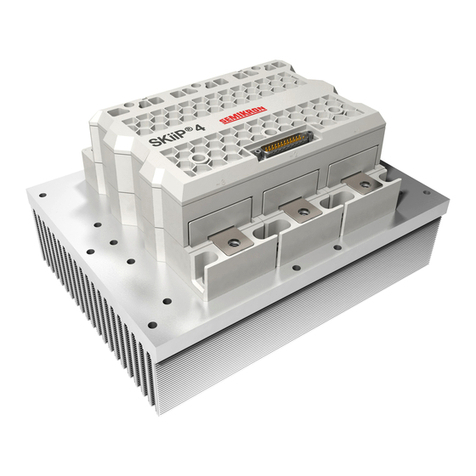
SEMIKRON SKYPER 42 LJ R User manual

© by SEMIKRON / 2019-07-23 / Technical Explanation / SKYPER®42 LJ R
PROMGT.1026/ Rev.7/ Template Technical Explanation
Page 1/35
1. Introduction...............................................................................................................................2
2. Block Diagram and Application Example ........................................................................................3
2.1 Block diagram.......................................................................................................................3
2.2 Application example ..............................................................................................................4
2.2.1 Primary side ...................................................................................................................4
2.2.2 Secondary side ...............................................................................................................5
3. Dimensions and mechanical precautions........................................................................................8
3.1 Dimensions ..........................................................................................................................8
3.2 Plug-in connection .................................................................................................................8
3.3 Support post.........................................................................................................................9
3.4 Solder connection..................................................................................................................9
3.5 Handling instructions ........................................................................................................... 10
4. Interface Description................................................................................................................. 11
4.1 Footprint ............................................................................................................................ 11
4.2 Pin assignment ...................................................................................................................11
4.2.1 Pin assignment of pin header X10 | Primary side............................................................... 11
4.2.2 Pin assignment of pin header X100 | Secondary side | TOP ................................................ 12
4.2.3 Pin assignment of pin header X200 | Secondary side | BOT ................................................12
4.3 Power Supply | Primary side .................................................................................................13
4.4 Gate drive signals | Primary side ........................................................................................... 14
4.5 Filter selection, jitter and propagation delay time | Primary side ............................................... 15
4.6 Error output | Primary side ................................................................................................... 15
4.7 Error input | Primary side ..................................................................................................... 16
4.8Error mode selection | Primary side .......................................................................................17
4.9 External error input | Secondary side.....................................................................................17
4.10 Gate resistors | Secondary side.............................................................................................19
4.11 External boost capacitors | Secondary side ............................................................................. 20
5. Protection features ................................................................................................................... 21
5.1 Failure management............................................................................................................21
5.2 Dead time and Interlock.......................................................................................................23
5.3 Short pulse suppression (SPS) .............................................................................................. 24
5.4 Undervoltage lockout (UVLO)................................................................................................ 24
5.5 Dynamic short circuit protection by VCEsat-monitoring (DSCP)....................................................25
5.5.1 DSCP | Functional description ......................................................................................... 26
5.5.2 DSCP | Calculation hints ................................................................................................ 27
5.6Active clamping................................................................................................................... 27
5.7 Soft Off..............................................................................................................................28
5.8 Safe short circuit turn-off in multilevel topology ......................................................................29
6. Electrical characteristic.............................................................................................................. 29
7. Product Qualification ................................................................................................................. 30
8. Environmental conditions .......................................................................................................... 31
9. Marking...................................................................................................................................32
10. Change history.........................................................................................................................33
Technical Explanation
SKYPER®
42 LJ R
Revision:
12
Issue date:
2019-07-23
Prepared by:
Niklas Hofstötter
Reviewed by:
Daniel Obernöder
Approved by:
Marco Honsberg
Keyword: IGBT driver core

© by SEMIKRON / 2019-07-23 / Technical Explanation / SKYPER®42 LJ R
PROMGT.1026/ Rev.7/ Template Technical Explanation
Page 2/35
1. Introduction
The SKYPER®42 LJ R is a two-channel driver core, which combines high output power with highly-
integrated ASIC technology in a very compact design. Its high reliability and EMC robustness makes the
SKYPER®42 LJ R suitable for a wide range of applications and sectors of many industries. The SKYPER®42
LJ R is designed to control semiconductor power modules with gate charges of typically up to 20µC and
provides reinforced isolation for operating voltages of up to 1200V. The interaction of the well-coordinated
functionality with the integrated safety functions makes the SKYPER®42 LJ R to a reliable control for power
semiconductor modules in standard, multilevel or parallel operation.
Figure 1: SKYPER®42 LJ R
KEY FEATURES
Two output channels
2.75W output power per channel
±3 ns jitter per channel
Fully isolated secondary side power supply
Separately controlled positive and negative gate voltages
Selectable filter settings
Soft turn-off in case of any secondary side error event
Short pulse suppression (SPS)
Under voltage lockout (UVLO)
Dynamic short circuit protection (DSCP)
MTBF rate > 7.5 Million hours at full load
Selectable error management modes for standard and multilevel applications

© by SEMIKRON / 2019-07-23 / Technical Explanation / SKYPER®42 LJ R
PROMGT.1026/ Rev.7/ Template Technical Explanation
Page 3/35
2. Block Diagram and Application Example
2.1 Block diagram
Figure 2: SKYPER®42 LJ R | Block diagram
Power Supply
Management
Power Supply
Management
Short Pulse
Suppression
Interlock
Signal
Processing
Dead Time
Generation
Filter
Management
UVLO
Error
Management
Gate Drive
Management
Power Supply
Management
Error
Management
Error
Management
Gate Drive
Management
UVLO
DSCP
DSCP
UVLO
nERR_IN_TOP
nERR_IN_BOT
PWR_VS_P_BOT
PWR_GND_BOT
PWR_VS_N_BOT
PWR_VS_P_TOP
PWR_GND_TOP
PWR_VS_N_TOP
BOT_ON
BOT_OFF
BOT_SOFTOFF
CLMP_IN_BOT
VCE_IN_BOT
CFG_VCE_BOT
TOP_ON
TOP_OFF
TOP_SOFTOFF
CLMP_IN_TOP
VCE_IN_TOP
CFG_VCE_TOP
PWR_VS
PWR_GND
TOP_IN
BOT_IN
CFG_FLT
CFG_IDT
nERR_IN
nERR_OUT
CFG_ERR

© by SEMIKRON / 2019-07-23 / Technical Explanation / SKYPER®42 LJ R
PROMGT.1026/ Rev.7/ Template Technical Explanation
Page 4/35
2.2 Application example
Figure 3 and Figure 4 show a typical SKYPER®42 LJ R core setting for operating a semiconductor module in
half-bridge configuration. SEMIKRON’s highly-integrated ASICs –as utilized on this driver core –enable the
SKYPER®42 LJ R to be easily configured with only a few simple external circuits and in turn reducing the
project and development time as well as the cost.
2.2.1 Primary side
Figure 3: SKYPER®42 LJ R | Application example | Primary side
Table 1: SKYPER®42 LJ R | Application example | Primary side | Recommended values
Component
Value
Remark
CTOP_IN / CBOT_IN
1nF
Optional filter capacitors suppressing high-frequency signals.
For further information please refer to [3].
CBST
-
Optional boost capacitor, dimensioning according to chapter
4.11.
RTOP_IN / RBOT_IN
10kΩ
Optional pull-down resistors, for steady off-state of the
corresponding output, if no input signal is applied.
RnERR_OUT
4.75kΩ
Optional pull-up resistor, mandatory if error output is used.
Dimensioning according to chapter 4.6
CBST
SKYPER®42 LJ R
PWR_GNDX10:01
PWR_VSX10:09
CFG_FLTX10:06
PWR_VSX10:10
nERR_OUTX10:03
nERR_INX10:04
PWR_VS
TOP_INX10:07
PWR_GNDX10:01
nERR_OUT
TOP_IN
RnERR_OUT
CTOP_IN
RTOP_IN
BOT_INX10:08
PWR_GNDX10:01
BOT_IN
CBOT_IN
RBOT_IN
CFG_IDTX10:02
CFG_ERRX10:05
PWR_GNDX10:01PWR_GND

© by SEMIKRON / 2019-07-23 / Technical Explanation / SKYPER®42 LJ R
PROMGT.1026/ Rev.7/ Template Technical Explanation
Page 5/35
2.2.2 Secondary side
Figure 4: SKYPER®42 LJ R | Application example | Secondary side
DC+
RG(on)_TOP
RG(softoff)_TOP
RVCE_TOP DVCE_TOP
DGE_TOP
T1
SKYPER®42 LJ R
VCE_IN_TOP X100:02
TOP_ON X100:05
TOP_OFF X100:06
TOP_SOFTOFF X100:09
PWR_GND_TOP X100:08
RG(off)_TOP
RGE_TOP
CGE_TOP
VCE_IN_BOT X200:02
BOT_ON X200:05
BOT_OFF X200:06
BOT_SOFTOFF X200:09
PWR_GND_BOT X200:08
RG(on)_BOT
RG(softoff)_BOT
RVCE_BOT DVCE_BOT
DGE_BOT
T2
RG(off)_BOT
RGE_BOT
CGE_BOT
DC-
PWR_VS_P_TOP X100:03
nERR_IN_TOP X100:04
CFG_VCE_TOP X100:01
CLMP_IN_TOP X100:07
PWR_GND_TOP X100:08
PWR_VS_N_TOP X100:10
CBST(N)_TOP
R2_CFG_TOP
R1_CFG_TOP
CCFG_TOP
CBST(P)_TOP
PWR_VS_P_BOT X200:03
nERR_IN_BOT X200:04
CFG_VCE_BOT X200:01
CLMP_IN_BOT X200:07
PWR_GND_BOT X200:08
PWR_VS_N_BOT X200:10
CBST(N)_BOT
R2_CFG_BOT
CCFG_BOT
CBST(P)_BOT
R1_CFG_BOT

© by SEMIKRON / 2019-07-23 / Technical Explanation / SKYPER®42 LJ R
PROMGT.1026/ Rev.7/ Template Technical Explanation
Page 6/35
Table 2: SKYPER®42 LJ R | Application example | Secondary side | Recommended values
Component
Value
Remark
CBST(P)_TOP / CBST(N)_TOP
CBST(P)_BOT / CBST(N)_BOT
-
Optional boost capacitors, dimensioning according to chapter
4.11.
CCFG_TOP / CCFG_BOT
-
Optional capacitor to adjust the blanking time tbl(VCE) of the
dynamic short circuit protection function. Necessary, if DSCP
is used. Dimensioning according to chapter 5.5.
CGE_TOP / CGE_BOT
-
Optional capacitor to prevent gate oscillation in case of short
circuit events or in case of parallel operation of semiconductor
power modules. For further information please refer to [3].
DGE_TOP / DGE_BOT
Optional suppressor diode to prevent gate voltage
overshoots. For further information please refer to [3].
DVCE_TOP / DVCE_BOT
-
Optional high voltage diode for VCE-monitoring, mandatory if
DSCP is used. Dimensioning according to chapter 5.5.
R1_CFG_TOP / R1_CFG_BOT
≥ 10kΩ
Optional resistors to adjust the trip level VCE(ref) of the
dynamic short circuit protection, necessary if DCSP is used.
Dimensioning according to chapter 5.5.
R2_CFG_TOP / R2_CFG_BOT
-
Optional resistors to adjust the trip level VCE(ref) of the
dynamic short circuit protection, necessary if DCSP is used.
Dimensioning according to chapter 5.5.
RGE_TOP / RGE_BOT
10kΩ
Optional resistor to avoid an open gate of the semiconductor,
if the driver is not supplied. For further information refer to
[3].
RG(off)_TOP / RG(off)_BOT
RG(on)_TOP / RG(on)_BOT
≥ 1Ω
Necessary resistors to adjust the semiconductors’ turn-on
and turn-off behavior. Dimensioning according to chapter
4.10.
RG(softoff)_TOP
RG(softoff)_BOT
≥ 1Ω
Mandatory resistor to adjust the semiconductors’turn-off
behavior in case of soft turn-off. Dimensioning according to
chapter 4.10.
RVCE_TOP / RVCE_BOT
511Ω
Optional series resistor for VCE-monitoring, mandatory if
DSCP is used.

© by SEMIKRON / 2019-07-23 / Technical Explanation / SKYPER®42 LJ R
PROMGT.1026/ Rev.7/ Template Technical Explanation
Page 7/35
Referring to the application example shown in Figure 3 and Figure 4, Table 3 describes the settings made.
Table 3: SKYPER®42 LJ R | Application example | Settings
Function
Configuration
Remark
Chapter
Active clamping
Disabled
Disabled by connecting the pins
CLMP_IN_TOP and CLMP_IN_BOT to the
corresponding PWR_GND pins.
5.6
Bidirectional error
(=HALT)
Enabled
Enabled by connecting the pin
nERR_OUT to pin nERR_IN.
4.7
Dynamic short circuit
protection (DSCP)
Enabled at both output
channels
Enabled by connecting the pins
VCE_IN_TOP and VCE_IN_BOT to the
corresponding collectors of the
semiconductors through RVCE_TOP ,
DVCE_TOP and RVCE_BOT ,DVCE_BOT.
DSCP configuration via pins
CFG_VCE_TOP and CFG_VCE_BOT.
5.5
Dead time
2µs (typical value)
Selected by connecting pin CFG_IDT to
pin PWR_GND.
5.2
Error mode
Both output channel
switch immediately into
off-state in case of any
error condition.
Selected by connecting pin CFG_ERR to
pin PWR_GND.
5.1
Error propagation
delay time
700ns (typical value)
Fixed value.
5.1
External error (HALT)
Disabled at both output
channels
Disabled by connecting the pins
nERR_IN_TOP and nERR_IN_BOT to the
corresponding PWR_VS pins.
5.1
External error
propagation delay
time
600ns (typical value)
Fixed value.
5.1
Filter
Digital
Selected by connecting pin CFG_FLT to
pin PWR_VS.
5.3
Interlock
Enabled
Enabled by connecting pin CFG_IDT to
pin PWR_GND.
5.2
Jitter
±12.5ns (typical value)
Selected by connecting the pins
CFG_FLT to pin PWR_VS.
4.5
Short pulse
suppression (SPS)
390 ns (typical value)
Selected by connecting pin CFG_FLT to
pin PWR_VS.
5.3
Undervoltage lockout
(UVLO)
Always active on
primary and secondary
side
-
5.4

© by SEMIKRON / 2019-07-23 / Technical Explanation / SKYPER®42 LJ R
PROMGT.1026/ Rev.7/ Template Technical Explanation
Page 8/35
3. Dimensions and mechanical precautions
3.1 Dimensions
Figure 5: SKYPER®42 LJ R | Dimension drawing
All dimensions in mm. Please consider higher tolerances of connector position according to IPC A 610.
STEP file on request.
3.2 Plug-in connection
The SKYPER®42 LJ R provides simple electrical and mechanical connection to adapter or control boards by
its standard pin headers. The primary side and the two secondary side plug-in connectors are 10 pin dual
row 2.54mm pin headers. For a secure mechanical connection of the driver it is essential that the pin
headers can be fully supported by the female mating connectors.
SEMIKRON recommends the use of the following female mating connector:
Description
Shape
Manufacturer
Art. no.
(female) RM2.54 10p
SMD 2ROW
Suyin
254100FA
Using SMD type mating connectors allows optimized board layout especially for SEMIKRON’s spring contact
modules like SEMiX.
8,13
8.13
16,11max. 19.00
5,092.54
5,212.54
6,69
33,75
47,33
51,25
55,50
46,00
40,64
6.69
33.75
47.33
51.25
40,64
46.00
40.64
55.50
Ø3,2
A
A 2:1

© by SEMIKRON / 2019-07-23 / Technical Explanation / SKYPER®42 LJ R
PROMGT.1026/ Rev.7/ Template Technical Explanation
Page 9/35
3.3 Support post
To increase the mechanical connection between the SKYPER®42 LJ R driver and the adapter board, up to
two support posts could be additionally assembled. It is recommended to use at least one support post. If a
support post is used, make sure it has the correct length. A support post which is too short bends both the
driver and the adapter board when mounted, thus increasing mechanical stress. If the support post is too
long, the mating connectors may not fully support the pin header.
The mounting holes of the support post are located in the insulation area between the secondary sides of
the driver. To avoid reduction of creepage and clearance distances when utilizing such a support post, the
support posts must have a CTI 600 classification at least.
Example of a support post:
Description
Shape
Manufacturer
Art. no.
Nylon support post
Dual lock
Richco
DLMSPM-8-01 (>12mm)
Figure 6: SKYPER®42 LJ R | Support post
mounting holes for support posts draft of a supported driver on an adapter board
3.4 Solder connection
The SKYPER®42 LJ R driver core can be soldered directly onto an adapter or control board. It should be
noted that if the driver is placed too close to the adapter or control board, the clearance distances from the
driver’s primary to secondary side as well as the clearance distances between the secondary sides may be
reduced.
Soldering hints
•The solder’s temperature must not exceed 260°C and the solder time must not exceed 10 seconds.
•The ambient temperature must not exceed the specified maximum storage temperature of the driver.
•The solder joints should be in accordance to IPC A 610 Revision D (or later) - Class 3 (Acceptability of
Electronic Assemblies) to ensure an optimum connection between driver core and printed circuit
board.
•The driver is not suited for hot air, reflow or infrared reflow processes.

© by SEMIKRON / 2019-07-23 / Technical Explanation / SKYPER®42 LJ R
PROMGT.1026/ Rev.7/ Template Technical Explanation
Page 10/35
3.5 Handling instructions
Please ensure electric static discharge protection during handling. The driver should only be removed from
its original packaging immediately before mounting. When mounting the driver it has to be ensured that
the work is done in an ESD-protected workplace. Persons working with the driver have to wear ESD
wristbands, overalls and shoes. If tools are used for mounting, those must comply with ESD standards.
When handling the driver, do not pick up the driver at the transformers. The driver MUST be handled at the
PCB sides.
Figure 7: SKYPER®42 LJ R | Handling instruction

© by SEMIKRON / 2019-07-23 / Technical Explanation / SKYPER®42 LJ R
PROMGT.1026/ Rev.7/ Template Technical Explanation
Page 11/35
4. Interface Description
4.1 Footprint
The footprint of the SKYPER®42 LJ R with its primary side pin header X10 and the secondary side pin
headers X100 and X200 are shown in Figure 8.
Figure 8: SKYPER®42 LJ R | Footprint | Bottom view
4.2 Pin assignment
4.2.1 Pin assignment of pin header X10 | Primary side
Table 4: SKYPER®42 LJ R | Pin assignment –Primary side | X10
Pin
Signal
Function
Specification
X10:01
PWR_GND
Ground potential for power
supply and digital signals
To be connected to ground
X10:02
CFG_IDT
Interlock dead time
configuration
15V logic; 150kΩ (pull-up)
LOW = 2µs interlock dead time
HIGH = No interlock dead time
X10:03
nERR_OUT
Error output
Open collector output; max. 18V/15mA
(external pull-up resistor needed)
LOW = Error
HIGH = No error
X10:04
nERR_IN
Error input
15V logic inverted; 150kΩ/10nF (pull-up)
LOW = External error
HIGH = No external error
X10:05
CFG_ERR
Error behaviour
configuration in case of any
error condition
15V logic; 150kΩ (pull-down)
LOW = Outputs switch off immediately
HIGH = Outputs switch off with next
turn-off signal at the
corresponding input
X10:06
CFG_FLT
Filter configuration for
switching signals
15V logic; 150kΩ (pull-down)
LOW = Analogue filter (tSPS(ana))
HIGH = Digital filter (tSPS(dig))
X10:07
TOP_IN
Switching signal input (TOP)
15V logic; 33kΩ/0.01nF (pull-down)
LOW = TOP switch off
HIGH = TOP switch on
X200
X100
X10
1
10
1
10
1
10

© by SEMIKRON / 2019-07-23 / Technical Explanation / SKYPER®42 LJ R
PROMGT.1026/ Rev.7/ Template Technical Explanation
Page 12/35
X10:08
BOT_IN
Switching signal input (BOT)
15V logic; 33kΩ/0.01nF (pull-down)
LOW = BOT switch off
HIGH = BOT switch on
X10:09
PWR_VS
Driver power supply
Stabilised +15V ±4%
X10:10
PWR_VS
Driver power supply
Stabilised +15V ±4%
4.2.2 Pin assignment of pin header X100 | Secondary side | TOP
Table 5: SKYPER®42 LJ R | Pin assignment –Secondary side | TOP | X100
Pin
Signal
Function
Specification
X100:01
CFG_VCE_TOP
VCE-monitoring reference
voltage
External voltage divider needed
X100:02
VCE_IN_TOP
VCE-monitoring input
External blocking diode needed
X100:03
PWR_VS_P_TOP
Power supply output,
positive voltage
Equal to VG(on)
(external buffer capacitors can be
connected)
X100:04
nERR_IN_TOP
External error input
15V logic inverted; 150kΩ/0.01nF (pull-up)
LOW = External error
HIGH = No external error
X100:05
TOP_ON
On signal path to TOP
semiconductor
External gate resistor needed
(in consideration of Iout(avg), Iout(peak), VG(on))
X100:06
TOP_OFF
Off signal path to TOP
semiconductor
External gate resistor needed
(in consideration of -Iout(avg), -Iout(peak),
VG(off))
X100:07
CLMP_IN_TOP
VCE-clamping input
150kΩ/0.01nF (pull-down)
In case of activated TOP_OFF:
LOW = TOP_OFF equal to VG(off)
HIGH = TOP_OFF floating
X100:08
PWR_GND_TOP
Ground potential for power
supply and digital signals
Reference potential for gate voltages
(emitter/source of power semiconductor)
X100:09
TOP_SOFTOFF
SoftOff signal path to TOP
semiconductor
External gate resistor needed
X100:10
PWR_VS_N_TOP
Power supply output,
negative voltage
Equal to VG(off)
(external buffer capacitors can be
connected)
4.2.3 Pin assignment of pin header X200 | Secondary side | BOT
Table 6: SKYPER®42 LJ R | Pin assignment –Secondary side |BOT | X200
Pin
Signal
Function
Specification
X200:01
CFG_VCE_BOT
VCE-monitoring reference
voltage
External voltage divider needed
X200:02
VCE_IN_BOT
VCE-monitoring input
External blocking diode needed
X200:03
PWR_VS_P_BOT
Power supply output,
positive voltage
Equal to VG(on)
(external buffer capacitors can be
connected)

© by SEMIKRON / 2019-07-23 / Technical Explanation / SKYPER®42 LJ R
PROMGT.1026/ Rev.7/ Template Technical Explanation
Page 13/35
X200:04
nERR_IN_BOT
External error input
15V logic inverted; 150kΩ/0.01nF (pull-up)
LOW = External error
HIGH = No external error
X200:05
BOT_ON
On signal path to BOT
semiconductor
External gate resistor needed
(in consideration of Iout(avg), Iout(peak), VG(on))
X200:06
BOT_OFF
Off signal path to BOT
semiconductor
External gate resistor needed
(in consideration of -Iout(avg), -Iout(peak),
VG(off))
X200:07
CLMP_IN_BOT
VCE-clamping input
150kΩ/0.01nF (pull-down)
In case of activated BOT_OFF:
LOW = BOT_OFF equal to VG(off)
HIGH = BOT_OFF floating
X200:08
PWR_GND_BOT
Ground potential for power
supply and digital signals
Reference potential for gate voltages
(emitter/source of power semiconductor)
X200:09
BOT_SOFTOFF
SoftOff signal path to BOT
semiconductor
External gate resistor needed
X200:10
PWR_VS_N_BOT
Power supply output,
negative voltage
Equal to VG(off)
(external buffer capacitors can be
connected)
4.3 Power Supply | Primary side
For a proper operation of the SKYPER®42 LJ R driver core, a power supply of at least 15W/1A shall be
connected to the driver’s power supply pins. During power-up of the driver turn-on signals shall not be
applied to the driver’s inputs TOP_IN/BOT_IN, otherwise the driver will not leave error state.
Please note, when controlling power semiconductor modules with a gate charge ≥ 2.5 µC external boost
capacitors are recommended on the primary side. Dimensioning of the boost capacitors according to
chapter 4.11.
Figure 9: SKYPER®42 LJ R | Primary side | Power supply
SKYPER®42 LJ R
CBST
PWR_VS
PWR_GND PWR_GNDX10:01
PWR_VSX10:10
PWR_VSX10:09

© by SEMIKRON / 2019-07-23 / Technical Explanation / SKYPER®42 LJ R
PROMGT.1026/ Rev.7/ Template Technical Explanation
Page 14/35
4.4 Gate drive signals | Primary side
The signal inputs TOP_IN/BOT_IN of the SKYPER®42 LJ R driver core have a +15V schmitt trigger logic. A
HIGH signal at the input of the driver leads to a switch-on command at the corresponding output of the
driver. A LOW signal at the input leads to a switch-off command at the corresponding output. Pulses below
1µs are not allowed.
Short pulses as well as voltage peaks, e.g. caused by interference, are suppressed by the driver and will
not be transmitted to the outputs. Further information to the short pulse suppression can be found in
chapter 5.3.
Figure 10: SKYPER®42 LJ R | Primary side | Gate drive signals
When using the driver in environments with high levels of electromagnetic noise, it is recommended to
connect a filter capacitor (CTOP_IN/CBOT_IN) of several hundred pico Farads as close as possible to the signal
inputs of the driver. Please note that these capacitors affect the propagation delay time of the driver. The
RTOP_IN/RBOT_IN resistors pull the inputs to low-level when no control signals are applied. The recommended
value of the pull-down resistors is approximately 10kΩ.
Parameter
Min
Typ
Max
Threshold high
-
-
10V
Threshold low
5V
-
-
SKYPER®42 LJ R
CTOP_IN
TOP_IN
PWR_GND
RTOP_IN
PWR_GNDX10:01
TOP_INX10:07
CBOT_IN
BOT_IN
PWR_GND
RBOT_IN
PWR_GNDX10:01
BOT_INX10:08

© by SEMIKRON / 2019-07-23 / Technical Explanation / SKYPER®42 LJ R
PROMGT.1026/ Rev.7/ Template Technical Explanation
Page 15/35
4.5 Filter selection, jitter and propagation delay time | Primary side
Due to SEMIKRON’s highly-integrated mixed signal ASICs the SKYPER®42 LJ R offers the freedom to select
filter type, jitter and propagation delay time to meet specific requirements of the application.
The filter time can be set via the configuration pin CFG_FLT. Connecting the CFG_FLT pin to the PWR_VS
pin enables the digital filter employing very low tolerances over the full temperature range.
Especially when using the driver in parallel operation the absolute deviation of the signal propagation delay
time from the input to the output is a key parameter. Depending on the settings made the SKYPER®42 LJ
R driver provides a very low jitter of typically ±3ns. Therefore the analogue filter has to be enabled and the
driver’s internal dead time generator has to be set to inactive. The dead time generator is inactive, if either
the interlock feature is disabled via the CFG_IDT pin or the dead time of the applied pulse pattern is longer
than 2µs. A detailed description of the interlock function and the dead time generation could be found in
chapter 5.2.
CFG_FLT
CFG_IDT
Setting
Filter time
Delay time
Jitter
HIGH
HIGH/LOW
Digital filter
390ns
830ns
±12.5ns
LOW
HIGH
Analogue filter
200ns
500ns
±3ns /±12.5ns
LOW
LOW
Analogue filter
200ns
500ns
±3ns
4.6 Error output | Primary side
The SKYPER®42 LJ R reports any detected error event at the nERR_OUT pin by pulling it to low-level. The
error output is an open collector output and requires an external pull-up resistor (RnERR_OUT). The
recommended value of the pull-up resistor is in the range of
.
As long as the driver has not been reset the error output will be at low-level.
A detailed description, how to reset the driver to end the error state and resume to operation is described
in chapter 5.1.
Figure 11: SKYPER®42 LJ R | Primary side | Error output
SKYPER®42 LJ R
PWR_VS
nERR_OUT nERR_OUTX10:03
PWR_VSX10:09
PWR_GND PWR_GNDX10:01
RnERR_OUT

© by SEMIKRON / 2019-07-23 / Technical Explanation / SKYPER®42 LJ R
PROMGT.1026/ Rev.7/ Template Technical Explanation
Page 16/35
4.7 Error input | Primary side
The nERR_IN input could be used to report an external error event to the SKYPER® 42 LJ R. If the nERR_IN
input is pulled to low-level the driver enters the error state. Depending on the error mode configuration,
described in chapter 4.8, the driver sets its outputs either immediately or with the next turn-off command
to low-level and locks them. After reset, as described in chapter 5.1, the driver is ready for operation,
again. If no reporting to the external error input is required, the nERR_IN input can be connected to the
PWR_VS pin or to the nERR_OUT pin.
In multiphase or parallel operation the nERR_IN input offers the possibility to force the outputs of each
driver in the system to off-state and locks them, simultaneously, without the need of an external control
unit. Therefore all nERR_OUT outputs and all nERR_IN inputs have to be connected together forming a
common bi-directional HALT line. Additionally, all CFG_ERR configuration pins have to be connected to
ground potential, as shown in Figure 12. In this configuration, any driver connected to the HALT line can
force the outputs of all connected drivers to off-state and locks them, when the driver pulls its nERR_OUT
output to low-level.
If a specific turn-off sequence is required –as it is common practice in NPC multilevel applications –the
configuration pins CFG_ERR have to be connected to the PWR_VS pins. A low-level of the HALT line locks
the outputs of the connected drivers, but does not immediately force them to low-level. The switched-on
outputs can be forced to off-state by the controller sending a switch-off command to the corresponding
signal inputs TOP_IN/BOT_IN.
If the driver is used in environments with high levels of interference, it is recommended to connect a filter
capacitor of approx. 10nF as close as possible to the nERR_IN pin and the PWR_GND pin.
Figure 12: SKYPER®42 LJ R | Primary side | Error input
Parameter
Min
Typ
Max
Threshold high
-
-
11 V
Threshold low
7.5 V
-
-
SKYPER®42 LJ R | 1
PWR_VS
nERR_OUT nERR_OUTX10:03
PWR_VSX10:09
PWR_GNDX10:01
RnERR_OUT
SKYPER®42 LJ R | 2
nERR_OUTX10:03
nERR_INX10:04
PWR_GND PWR_GNDX10:01
nERR_INX10:04
X10:05 CFG_ERR
X10:05 CFG_ERR

© by SEMIKRON / 2019-07-23 / Technical Explanation / SKYPER®42 LJ R
PROMGT.1026/ Rev.7/ Template Technical Explanation
Page 17/35
4.8 Error mode selection | Primary side
The behaviour of the SKYPER®42 LJ R driver core on an error event can be selected via the configuration
pin CFG_ERR.
Connecting the CFG_ERR pin to the PWR_GND pin forces the driver to set its outputs to off-state
immediately when an error is detected. As long as the driver has not been reset the error event is reported
at the corresponding terminal and the driver’s outputs are kept locked. Whereby, depending on whether an
error is detected on the primary or on the secondary side the driver switches off the connected
semiconductors via the standard turn-off or the soft-off path. If an error occurs on the primary side the
driver will activate the standard turn-off paths of both channels. If an error occurs on the secondary side,
the driver will activate the soft-off path of the affected secondary side. The semiconductor connected to the
other secondary side will be switched off with the standard turn-off procedure.
If the CFG_ERR pin is connected to the PWR_VS pin, the driver locks its outputs in case of any error event
and, hence, reports the error event at the terminal nERR_OUT, but the driver will not be set the outputs to
off-state, immediately. The outputs will be set to off-state, when the driver has received a turn-off
command at the corresponding signal input TOP_OFF/BOT_OFF. Depending on whether an error is detected
on the primary or secondary side the driver activates the standard turn-off or the soft-off path, as
described above.
Further information related to the primary and secondary error events, as well as on the error reset
conditions can be found in chapter 5.1.
Parameter
Min
Typ
Max
Threshold high
-
-
11 V
Threshold low
7.5 V
-
-
4.9 External error input | Secondary side
Each secondary side of the driver provides an error input (nERR_IN_TOP/nERR_IN_BOT) to handle an
external error event. These inputs are low active. Pulling one input to low-level forces the driver into error
state. The behaviour of the driver in case of an external error event depends on the configuration done via
the configuration pin CFG_ERR, as described in chapter 4.8.
The external error input is typically used to monitor temperature, current or voltage of modules, phase legs
or systems. The error input of the secondary TOP side can be disabled by connecting it to the
PWR_VS_P_TOP pin the error input of the secondary BOT side by connecting it to the PWR_VS_P_BOT pin.
Figure 13 shows a recommended circuitry of an over temperature detection by NTC resistor monitoring. If
the voltage at the positive input of the comparator falls below the voltage level at the comparator’s
negative input the comparator will set the nERR_IN input to low-level and will generate an external error
event. Assuming that resistor R3and R4have the same value the comparator’s trip level is reached when
the value of the NTC falls below the value of RCGF(temp). Please note that the negative supply pin of the
comparator is connected to PWR_VS_N which has to be taken into account, in case the NTC thermistor is
monitored by an external application circuit as well.

© by SEMIKRON / 2019-07-23 / Technical Explanation / SKYPER®42 LJ R
PROMGT.1026/ Rev.7/ Template Technical Explanation
Page 18/35
Figure 13: SKYPER®42 LJ R | Secondary side | Example of an external error input circuitry
Recommended values
Component
Value
Remark
C1
1nF
C2
100nF
C3
1µF
R1
30.1kΩ
R2
15kΩ
R3
30.1kΩ
R4
30.1kΩ
RCFG(temp)
-
The value of the RCFG(temp) has to be determined considering
the resistance characteristic of the connected thermistor and
the desired trip level.
Parameter
Min
Typ
Max
Threshold high
-
-
13 V
Threshold low
2 V
-
-
R1
SKYPER®42 LJ R
PWR_VS_P_TOP X100:03
nERR_IN_TOP X100:04
PWR_GND_TOP X100:08
PWR_VS_N_TOP X100:10
ϑ
R2
C1
C2
RCFG(temp)
C3
R3
R4

© by SEMIKRON / 2019-07-23 / Technical Explanation / SKYPER®42 LJ R
PROMGT.1026/ Rev.7/ Template Technical Explanation
Page 19/35
4.10 Gate resistors | Secondary side
The SKYPER®42 LJ R driver has three outputs channels at each secondary side
(TOP_ON/TOP_OFF/TOP_SOFTOFF and BOT_ON/BOT_OFF/BOT_SOFTOFF) to provide the possibility of
separate optimization of the semiconductor’s turn-on and turn-off behavior. By default, the driver uses the
TOP_OFF and BOT_OFF output to turn-off of the semiconductor. The SOFTOFF output will be activated by
the driver in case a secondary side error event was detected to ensure a soft turn-off of the connected
semiconductor, which in turn shall prevent voltage overshoots and protect the semiconductor against
destruction. Therefore it is mandatory to populate a suitable soft-off gate resistor since otherwise the driver
cannot turn-off the semiconductor via the soft-off path. A detailed explanation of when the driver is
activating the soft-off path is given in chapter 4.8.
The gate resistor influences the IGBT switching time, switching losses, reverse bias safe operating area
(RBSOA), short-circuit safe operating area (SCSOA), EMI, dv/dt, di/dt and reverse recovery current of the
freewheeling diode. It has to be selected and optimized very carefully in accordance with the individual
application parameters, e.g. IGBT technology, diode, switching frequency, losses, application layout,
inductivity / stray inductance, DC-link voltage and driver capability. The complete design of an application
must be viewed as a whole, with due considering of the above-mentioned parameters at least. Interactive
effects within the whole application must be evaluated and accommodated. [4]
The minimum value of the gate resistors RG(on) and RG(off) could be calculated by the following equation:
.
The minimum value of the RG(softoff) is 1Ω. Additional hints how to determine the values of the gate resistors
are given in [4].
Figure 14: SKYPER®42 LJ R | Secondary side | Gate resistors
Please note that some of SEMIKRON’s driver cores using an ASIC internal N-channel MOSFET for Soft Off.
To protect this MOSFET against back swings when turning-off the TOP_ON/BOT_ON channel it is
recommended to place the RG(softoff) resistor in series to the RG(off) resistor.
Since each turn-on and turn-off of a semiconductor means charging or discharging the parasitic input
capacitance of the semiconductor, the gate resistor has to be pulse load proofed. For this reason
SEMIKORN recommends the use of following resistors.
Description
Shape
Manufacturer
Art. no.
MELF resistors
MELF / MiniMELF SMD
Vishay Beyschlag,
Vishay Draloric,
Vitrohm
PRO MELF resistors,
SMM0207, SMM 0204,
ZCM series
DC+
RG(on)_TOP
RG(softoff)_TOP
T1
SKYPER®42 LJ R
TOP_ON X100:05
TOP_OFF X100:06
TOP_SOFTOFF X100:09
PWR_GND_TOP X100:08
RG(off)_TOP
AC
RG(int)_TOP
RE_TOP
IGBT

© by SEMIKRON / 2019-07-23 / Technical Explanation / SKYPER®42 LJ R
PROMGT.1026/ Rev.7/ Template Technical Explanation
Page 20/35
4.11 External boost capacitors | Secondary side
The SKYPER®42 LJ R allows driving of semiconductor power modules with a gate charge (QG) of up to
20µC per output. To stabilize the gate voltages VG(on) and VG(off) during the semiconductor switches the use
of boost capacitors per channel are recommended, if the connected gate charge is larger than 2.5µC. These
capacitors has to be placed as close as possible to the driver, as shown in Figure 15.
Figure 15: SKYPER®42 LJ R | Secondary side | Boost capacitors
The external boost capacitors can be calculated by following equation:
Please note, when assembling boost capacitors at the secondary side, also boost capacitors has to be
assembled at the primary side, as shown in Figure 9.
SKYPER®42 LJ R
CBST(N)_TOP
CBST(P)_TOP
PWR_VS_P_TOP X100:03
PWR_GND_TOP X100:08
PWR_VS_N_TOP X100:10
This manual suits for next models
1
Table of contents
Other SEMIKRON Control Unit manuals
