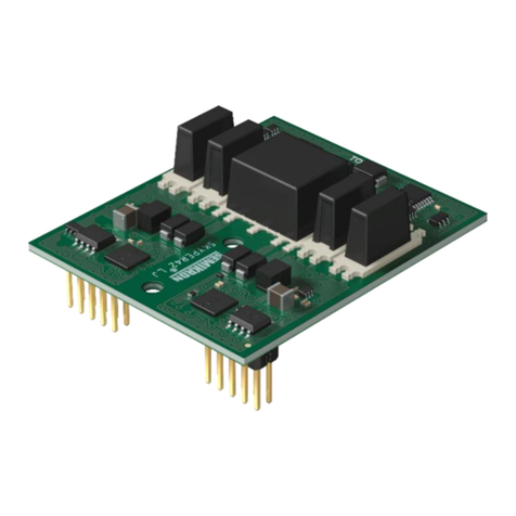
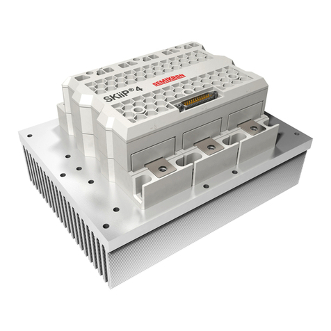
SEMIKRON SKiiP 4 F L5066401 User manual

Technical
Explanation
© by SEMIKRON
PROMGT.1026 / Rev. 1 / Template Technical
Explanation
2017-08-30 - Rev02
1 / 21
This document is valid for the following part numbers:
- L5066401 SKiiP®4 F-Option with D-Sub connector, no plastic case
- L5066402 SKiiP®4 F-Option with D-Sub connector
- L5066403 SKiiP®4 F-Option without D-Sub connector
Technical Explanation SKiiP®4 F-Option Board
Revision:
02
Issue Date:
2017-08-30
Prepared by:
Schiller Anastasia
Approved by:
AG E-KAZ
SKiiP®4 F-Option Board
Please note:
Unless otherwise specified, all values in this technical explanation are typical values. Typical values are the average values
expected in large quantities and are provided for information purposes only. These values can and do vary in different applications.
All operating parameters should be validated by user’s technical experts for each application.
The document remains effective until replaced by subsequent revision of this document.

Technical Explanation
SKiiP®4 F-Option Board
© by SEMIKRON
2017-08-30 - Rev02
2 / 21
Table of content:
1Related documents .........................................................................................................................................3
2Application and handling instructions..............................................................................................................4
3General description .........................................................................................................................................5
4Block diagram..................................................................................................................................................6
5Dimensions......................................................................................................................................................7
6Mounting Instruction......................................................................................................................................10
6.1 Mounting Instruction for F-Option Board Variants 2 and 3.....................................................................10
6.2 Mounting Instruction for F-Option Board Variant 1.................................................................................12
7Description of D-Sub connector X2...............................................................................................................12
7.1 Pin Description........................................................................................................................................12
7.2 Not used Signals.....................................................................................................................................13
8Pin Description of optical connectors X4, X5, X6..........................................................................................13
9Power Supply ................................................................................................................................................13
10 Optical Input/Output Signals..........................................................................................................................14
10.1 PWM TOP/BOT Signals .........................................................................................................................14
10.2 ERROR_OUT Signal ..............................................................................................................................15
11 D-Sub Connector signals ..............................................................................................................................16
11.1 HALT Signal............................................................................................................................................16
11.2 GPIO Signal............................................................................................................................................17
11.3 Analogue Signals....................................................................................................................................17
11.4 CAN Signals............................................................................................................................................17
12 Logistics.........................................................................................................................................................18
13 Provisions and handling after use.................................................................................................................19

Technical Explanation
SKiiP®4 F-Option Board
© by SEMIKRON
2017-08-30 - Rev02
3 / 21
1 Related documents
Technical Explanation SKiiP®4, Rev. 3
CANopen User Manual Rev.6
Data sheets SKiiP®4
Data sheets SKiiP®4 F-Option
Data sheets SKHBP SKiiP®4
Technical Explanation SKiiP®4 Parallel Board

Technical Explanation
SKiiP®4 F-Option Board
© by SEMIKRON
2017-08-30 - Rev02
4 / 21
2 Application and handling instructions
Please provide static discharge protection during handling. As long as the board is not completely
assembled, the input terminals have to be short-circuited. Persons working with devices have to wear a
grounded bracelet. Any synthetic floor coverings must not be statically chargeable. Even during
transportation the input terminals have to be short-circuited using, for example, conductive rubber.
Worktables have to be grounded.
When first operating a newly developed circuit, SEMIKRON recommends to apply low collector voltage
and load current in the beginning and to increase these values gradually, observing the turn-off
behavior of the free-wheeling diode and the turn-off voltage spikes generated across the IGBT. An
oscillographic control will be necessary. Additionally, the case temperature of the module has to be
monitored. When the circuit works correctly under rated operation conditions, short-circuit testing may
be done, starting again with low collector voltage.
It is important to feed any errors back to the control circuit and to switch off the device immediately in
failure events. Repeated turn-on of the IGBT into a short circuit with a high frequency may destroy the
device.

Technical Explanation
SKiiP®4 F-Option Board
© by SEMIKRON
2017-08-30 - Rev02
5 / 21
3 General description
The SKiiP®4 F-Option Board allows the controlling of SKiiP®4 system by means of fiber optics. There are three
variants of SKiiP®4 F-Option available:
- Variant 1: L5066401 SKiiP®4 F-Option with D-Sub connector, no plastic case
- Variant 2: L5066402 SKiiP®4 F-Option with D-Sub connector
- Variant 3: L5066403 SKiiP®4 F-Option without D-Sub connector
In case of using SKiiP®4 F-Option the two switching signals (TOP/BOT) and the GPIO error signal are
transferred via optical connection. In addition the analogue signals as well as the CAN-Bus signals are
available on the D-Sub connector X2 for Variants 1 and 2 of F-option boards described above.
The electrical connection between SKiiP®4 F-Option board and SKiiP®4 driver must be realized by 25-wired
ribbon cable. The built-in connector of the SKiiP®4 F-Option board can be directly plugged in case of mounting
SKiiP®4 F-Option on the SKiiP®4 top cover (Variants 2 and 3) or on SKiiP®4 Paralleling Board (Variant 1). In
other cases the usage of cable extention up to 1,5m is allowed. On the other side it must always be connected
to the SEMIKRON “SKiFace Standard” interface of SKiiP®4 driver by a 25-pin D-Sub female connector. Please
refer to the Technical Explanation SKiiP®4 for pin assignment of connector X1.
The example of SKiiP®4 F-Option board application for Variant 1 is shown in the Figure 3.1.
Figure 3.1: SKiiP4 F-Option board (Variant 1) application example with connected SKiiP®4 system
Please note that in case of mounting SKiiP®4 F-Option board (Variant 1) on the SKiiP®4 Parallel board the
SKiiP®4 Parallel board variant compatible to the F-Option board should be chosen. The following SKiiP®4
Parallel boards are compatible to the F-Option Board (Variant 1):
L5064204 (paralleling of 4 SKiiP®4 systems),
L5064205 (paralleling of 3 SKiiP®4 systems),
L5064206 (paralleling of 2 SKiiP®4 systems).
Pollution degree class 2 and IP00 shall be considered for all SKiiP®4 F-Option boards.

Technical Explanation
SKiiP®4 F-Option Board
© by SEMIKRON
2017-08-30 - Rev02
6 / 21
4 Block diagram
Figure 4.1: Block diagram of SKiiP®4 F-Option board main functions
TOP/BOT
optical signals
CMN_DCL
CMN_TEMP
HB_I
PWR_VS
HB_TOP/
HB_BOT
ERROR_OUT
optical signal
X4/X6 X1 (SKiFace)
SKiiP4 F-Option
CAN-Bus
Current
measurement
Temperature
measurement
DC-Link
measurement
CAN-Bus
X2
+24V
X5
X3 Power supply
F-BLOCK 1
F-BLOCK 2
F-BLOCK 3
CMN_GPIO
HALT
GPIO
+24V
Converting of GPIO
signal from SKiiP4 to
optical signal
CMN_HALT
or
F-BLOCK 4
F-BLOCK 5
Converting of optical TOP/BOT signals
to SKiFace Standard Signals
Only available for
Variants 1 and 2
The main functions of the SKiiP®4 F-Option board are shown in the Figure 4.1. They are:
F-Block 1: Converting the optical TOP/BOT switching signals from the connectors X4/X6 to the SKiiP®4
connector X1
F-Block 2: Converting the GPIO signal from SKiiP®4 connector X1 to optical error signal ERROR_OUT
at connector X5
F-Block 3: +24V power supply
The F-Blocks 4 and 5 as well as +24V routing from controller connector X2 to SKiiP®4 connector X1 (please
see Chapter 9 for details) are available only for F-Option Variants 1 and 2:
F-Block 4: Forwarding of analogue signals from SKiiP®4 connector X1 to F-Option D-Sub connector X2
F-Block 5: Forwarding of CAN-Bus signals from SKiiP®4 connector X1 to F-Option D-Sub connector X2
HALT and GPIO Signals are available on the F-Option D-Sub connector X2 as well.

Technical Explanation
SKiiP®4 F-Option Board
© by SEMIKRON
2017-08-30 - Rev02
7 / 21
5 Dimensions
The mechanical dimensions of SKiiP®4 F-Option board Variant 1, top view are shown in the Figure 5.1.
Figure 5.1: Mechanical dimensions of SKiiP®4 F-option board Variant 1, top view
The mechanical dimensions of SKiiP®4 F-Option board Variant 1, side view are shown in the Figure 5.6.
Figure 5.2: Mechanical dimensions of SKiiP®4 F-option board Variant 1, side view

Technical Explanation
SKiiP®4 F-Option Board
© by SEMIKRON
2017-08-30 - Rev02
8 / 21
The mechanical dimensions of SKiiP®4 F-Option board Variant 2, top view are shown in the Figure 5.3.
Figure 5.3: Mechanical dimensions of SKiiP®4 F-option board Variant 2, top view
The mechanical dimensions of SKiiP®4 F-Option board Variant 2, side view are shown in the Figure 5.4.
Figure 5.4: Mechanical dimensions of SKiiP®4 F-option board Variant 2, side view

Technical Explanation
SKiiP®4 F-Option Board
© by SEMIKRON
2017-08-30 - Rev02
9 / 21
The mechanical dimensions of SKiiP®4 F-Option board Variant 3, top view are shown in the Figure 5.5.
Figure 5.5: Mechanical dimensions of SKiiP®4 F-option board Variant 3, top view
The mechanical dimensions of SKiiP®4 F-Option board Variant 3, side view are shown in the Figure 5.6.
Figure 5.6: Mechanical dimensions of SKiiP®4 F-option board Variant 3, side view

Technical Explanation
SKiiP®4 F-Option Board
© by SEMIKRON
2017-08-30 - Rev02
10 / 21
6 Mounting Instruction
6.1 Mounting Instruction for F-Option Board Variants 2 and 3
The mounting process for both Variants 2 and 3 is identic, the description below is shown on example of F-
Option board Variants 2.
The F-Option plastic housing consists of two parts: bottom part (Figure 6.1, left) and top cover (Figure 6.3, left).
1. The bottom part should be placed on the SKiiP®4 top cover so that the snap-fits with larger distance (see
green arrows Figure 6.1) match to the slots of SKiiP®4 top cover. Afterwards the other side should be
pressed inside applying slight pressure (see red arrows Figure 6.1) till the click is audible.
Figure 6.1: Mounting of bottom part of plastic cover SKiiP4 F-option board
2. The PCB can now be inserted in the bottom part of the F-Option housing (Figure 6.2), where it will be fixed
by pressure parts at the sides (see blue arrows Figure 6.2). One edge of the PCB and housing is cut off
(see red arrow Figure 6.2) to avoid the reversed placing of PCB. It is recommended to insert the PCB into
the housing at the beginning on one side and then to press it inside on the other side applying slight
pressure. Please check the screw holes on PCB match to the holes of bottom part of plastic cover.

Technical Explanation
SKiiP®4 F-Option Board
© by SEMIKRON
2017-08-30 - Rev02
11 / 21
Figure 6.2: Inserting of the PCB inside the plastic cover
3. The next step is mounting of the top part of the plastic housing SKiiP®4 F-Option. Please take care that the
snap-fits of bottom part match to the snap-fits of the top cover of the housing (see red arrows Figure 6.3,
the cable connection between F-option Board and SKiiP®4 is not shown).
Figure 6.3: Mounting of the top part of the plastic cover SKiiP®4 F-option board

Technical Explanation
SKiiP®4 F-Option Board
© by SEMIKRON
2017-08-30 - Rev02
12 / 21
Figure 6.4: Mounting of the top part of the plastic cover SKiiP®4 F-option board, final view
4. The PCB should now be fixed with 4 screws Ejot Delta PT 40x18 T20, order number: 4230435809, in the
bottom part of the F-Option housing (please see Figure 6.4, blue arrows). Please use the screws included
in delivery. The screwing parameters should be set up as follows:
Screwer to be used (Bit): T20 Torx
Rpm: 500 –600 U\min
Torque for the first time screwing: 1,8 Nm
Torque for the next screwing (manually, without rpm control): 1,2 - 1,4 Nm
By inadequate setting of screwing parameters mounting problems can occur, e.g. loosing of top cover or
thread damage.
6.2 Mounting Instruction for F-Option Board Variant 1
Please refer to the Technical Explanation SKiiP®4 Parallel Board for information about mounting of F-Option
SKiiP®4 Variant 1 on the SKiiP®4 Parallel Board.
It is also possible to use F-Option SKiiP®4 Variant 1 as a spare part replacement for Varant 2. In this case it
must be inserted into the plastic housing as decribed in the chapter 6.1.
7 Description of D-Sub connector X2
7.1 Pin Description
Please refer to SKiiP®4 Technical Explanation Rev.3 Chapter 5.2 “Gate driver interface SkiFace” for further
information and pin out of connector X2.
Please note: Pin 8 HB_TOP and pin 21 HB_BOT are not connected!

Technical Explanation
SKiiP®4 F-Option Board
© by SEMIKRON
2017-08-30 - Rev02
13 / 21
7.2 Not used Signals
For more details please see Technical Explanation SKiiP®4 Rev.3 Chapter 5.2.11 ”Reserved or not used
signals”.
8 Pin Description of optical connectors X4, X5, X6
Table 1: Description of optical connectors X4, X5, X6
Connector
Type
Signal description
X4
Optical Receiver
Type: HFBR-2521ETZ, horizontal
Receives the PWM control signal for TOP-
IGBT from the controller
X5
Optical Transmitter
Type: HFBR-1521ETZ, horizontal
Transmits the GPIO error signal from SKiiP4
driver to controller
X6
Optical Receiver
Type: HFBR-2521ETZ, horizontal
Receives the PWM control signal for BOT-
IGBT from the controller
The following fiber optical cable type was used for the qualification: Leoni KHPS-HPS11005m. This fiber optic
cable consists of:
2 optical connectors SXHP-SSO-19-0040 (incl. crimp barrel)
5m long optical fiber cable V2Y 1P980/1000.
9 Power Supply
Please refer to SKiiP®4 Technical Explanation Rev.3 Chapter 5.2 “Gate driver interface SkiFace” for further
information and pin out of connector X2.
The pin assignment of power supply connector X3 is shown in the Table 2.
Table 2: Power supply connector X3 pin assignment
Pin
Signal name
Function
01
n.c.
02
GND
Ground
03
+24V
Supply voltage input for F-Option Board and SKiiP®4
Table 3 shows the required features of an appropriate power supply for a SKiiP®4 system.
Table 3: Requirements of the power supply
Power supply
Supply voltage should be +24V (+/- 20%). The supply is defined at the F-Option
Board input.
Maximum rise time of 24V
< 2s
Rated current
1.5 times of the maximum SKiiP driver input current
Minimum peak
2 times of the maximum SKiiP driver input current (at least 1,5A)
For further information please refer to the Technical Explanation SKiiP®4.
Please note: The supply voltage for SKiiP®4 F-Option Board and SKiiP®4 system can be provided over
power supply connector X2 if the voltage drop over the ribbon cable will not be too high due to the supply
current (please see data sheet SKiiP®4 for supply current formula). Otherwise supply connector X3
should be used.
Please note: Power supply cable should be twisted or shielded to enhance the EMI robustness.

Technical Explanation
SKiiP®4 F-Option Board
© by SEMIKRON
2017-08-30 - Rev02
14 / 21
10 Optical Input/Output Signals
10.1 PWM TOP/BOT Signals
The PWM TOP/BOT optical signals could be described as follow: by recognised incoming light the IGBT will be
switched on, by no light the IGBTwill be switched off. Please see Table 4.
Table 4: PWM TOP/BOT optical signals
Optical Receiver receives light
Optical Receiver receives no light
IGBT ON
IGBT OFF
Please note: A non-connected optical link will be considered as LOW signal (IGBT OFF).
If the light intensity is not sufficient the IGBT might stay off and an ERROR_OUT signal might be set. To avoid
this the minimal transmitter current IFdc at the controller side should be at least 50 mA. Please see Figure 10.1
for example of the circuit for transmitter LED at the controller side.
Figure 10.1:Transmitter current controller side

Technical Explanation
SKiiP®4 F-Option Board
© by SEMIKRON
2017-08-30 - Rev02
15 / 21
10.2 ERROR_OUT Signal
Characteristics and functionality:
Shows the status of the IGBT driver
For ERROR_OUT logic please see Table 5.
Table 5: ERROR_OUT optical signal
Optical Transmitterr emits light
Optical Transmitter emits no light
No error
Error
The connected SKiiP®4 system sets the ERROR-OUT signal (Optical transmitter emits no light) if following
happens:
the unit is not ready to operate
error happened
Please refer to the SKiiP®4 Technical Explanation Rev.3 chapter “GPIO -Signal” for further information.

Technical Explanation
SKiiP®4 F-Option Board
© by SEMIKRON
2017-08-30 - Rev02
16 / 21
Please note: D-Sub connector signals are available only for SKiiP®4 F-Option Board Variants 1 and 2.
Please note: maximal number of devices for paralleling of HALT signal is 6 items.
11 D-Sub Connector signals
11.1 HALT Signal
Figure 11.1 depicts:
on the left hand side the Input/Output stage of the CMN_HALT signal
on the right hand side an example of the input stage on the user controller board for each CMN_HALT
output of several SKiiP®4 with F-Option Boards.
Figure 11.1: Application example of the HALT signal
1k 20k
Driver Board including F-Option Board 1
to µC
from
µC
VS
Vcc µC
Transmitter
Receiver
10k
12.1k
20k
51k
24.3k
1k
User Controller Board
to µC
from
µC
Vcc µC
Transmitter
Receiver
PWR_VS
VS
to stopp all devices
to send HALT signal
to receive HALT
signal to receive HALT
signal
External
Power Supply
CMN_HALT
CMN_GND
30V 10n
1k
909Ω
(Pin 5)
1k
to µC
from
µC
VS
Vcc µC
Transmitter
Receiver
10k
12.1k
20k
51k
24.3k
1k
to µC
from
µC
Vcc µC
Transmitter
Receiver
PWR_VS
VS
to stopp all devices
to send HALT signal
to receive HALT
signal to receive HALT
signal
CMN_HALT
CMN_GND
30V 10n
1k
909Ω
(Pin 5)
6.19k
30V
30V
20n
20n
6.19k
20k
c
The HALT signals of all SKiiPs in the application and from other hardware components can also be connected
together. That means that the HALT signal is set to LOW state when one of the connected SKiiPs is not ready
to operate. In this case only one receiver circuit on the user controller board is necessary. In case of failure the
switch off time for all such connected susystems will be shorter, than for SKiiPs with separately processed
HALT-signals.

Technical Explanation
SKiiP®4 F-Option Board
© by SEMIKRON
2017-08-30 - Rev02
17 / 21
11.2 GPIO Signal
Figure 11.2 depicts:
on the left hand side the output stage of the CMN_GPIO signal
on the right hand side an example of the input stage on the user controller board for each CMN_GPIO
output of several SKiiP®4 with F-Option Boards.
Figure 11.2: Application example of the CMN_GPIO (inverted HALT signal) as error output signal
Driver Board including
F-Option Board 1
from µC
10k
12.1k
20k
24.3k
1k
User Controller Board
to µC
Vcc µC
PWR_VS
VS
External
Power Supply
CMN_GND
VS
1k
Driver Board including
F-Option Board n
from µC
VS
GPIO
CMN_GND
12.1k
20k
24.3k
1k
to µC
Vcc µC
VS
send GPIO signal
send GPIO signal
51k
10k51k
GPIO
30V 10n
30V 10n
20n
20n
30V
30V
6.19k
6.19k
11.3 Analogue Signals
F-Option Board with D-Sub-Connector forwards analogue signals without any changes. For signal
characteristics and further information please see Technical Explanation SKiiP®4 Rev.3 Chapter 5.3.8.
11.4 CAN Signals
F-Option Board with D-Sub-Connector forwards CAN signals without any changes. For more details please see
Technical Explanation SKiiP®4 Rev.3 Chapter 5.2.8 as well as the CANopen User Manual Rev.6.

Technical Explanation
SKiiP®4 F-Option Board
© by SEMIKRON
2017-08-30 - Rev02
18 / 21
12 Logistics
Figure 12.1: Part Marking Information

Technical Explanation
SKiiP®4 F-Option Board
© by SEMIKRON
2017-08-30 - Rev02
19 / 21
13 Provisions and handling after use
Components which are obsolete or defective must be disposed according to local regulations

Technical Explanation
SKiiP®4 F-Option Board
© by SEMIKRON
2017-08-30 - Rev02
20 / 21
List of figures:
Figure 3.1: SKiiP4 F-Option board application with connected SKiiP4 system......................................................5
Figure 4.1: Block diagram of SKiiP®4 F-Option board main functions ..................................................................6
Figure 5.1: Mechanical dimensions of SKiiP®4 F-option board, top view...............................................................7
Figure 5.2: Mechanical dimensions of SKiiP®4 F-option board, side view.............................................................9
Figure 6.1: Mounting of bottom part of plastic cover SKiiP4 F-option board....................................................... 10
Figure 6.2: Inserting of the PCB inside the plastic cover..................................................................................... 11
Figure 6.3: Mounting of the top part of the plastic cover SKiiP®4 F-option board.............................................. 11
Figure 6.4: Mounting of the top part of the plastic cover SKiiP®4 F-option board, final view.............................. 12
Figure 10.1:Transmitter current controller side.................................................................................................... 14
Figure 11.1: Application example of the HALT signal ......................................................................................... 16
Figure 11.2: Application example of the CMN_GPIO (inverted HALT signal) as error output signal.................. 17
Figure 12.1: Part Marking Information................................................................................................................. 18
List of tables:
Table 1: Description of optical connectors X4, X5, X6 ........................................................................................ 13
Table 2: Power supply connector X3 pin assignment ......................................................................................... 13
Table 3: Requirements of the power supply........................................................................................................ 13
Table 4: PWM TOP/BOT optical signals ............................................................................................................. 14
Table 5: ERROR_OUT optical signal .................................................................................................................. 15
References
[1] www.SEMIKRON.com
[2] A. Wintrich, U. Nicolai, W. Tursky, T. Reimann, “Application Manual Power Semiconductors”,
ISLE Verlag 2011, ISBN 978-3-938843-666
This manual suits for next models
2
Table of contents
Other SEMIKRON Control Unit manuals
Popular Control Unit manuals by other brands

Pentair
Pentair Fleck 4600 MECH user guide

Paso
Paso PM2044-B Instructions for use

STIEBEL ELTRON
STIEBEL ELTRON WPM Commissioning

Baker Hughes
Baker Hughes Consolidated 2700 Series instruction manual
Pfeiffer Vacuum
Pfeiffer Vacuum EVB 063 PA instruction sheet

Bristan
Bristan N2 SHCVO C Installation instructions & user guide

Jung
Jung BT 1001 Series operating instructions
Vega
Vega VEGADIS 81 operating instructions
Beckhoff
Beckhoff KM2002 Documentation
Helo
Helo WE 40 User and installation manual
National Instruments
National Instruments NI 9269 Getting started guide

KOGANEI CORPORATION
KOGANEI CORPORATION HV160E1-2 instruction manual
