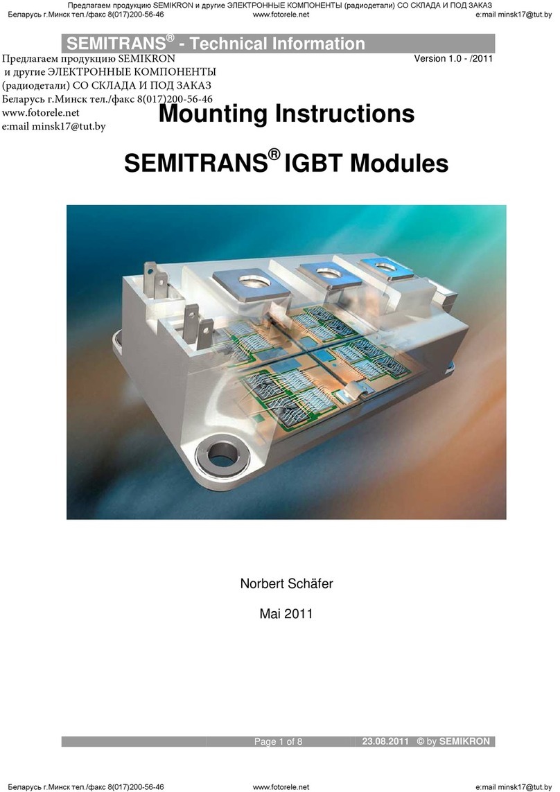
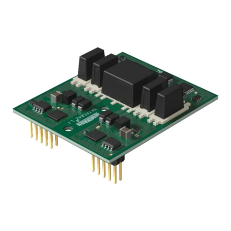
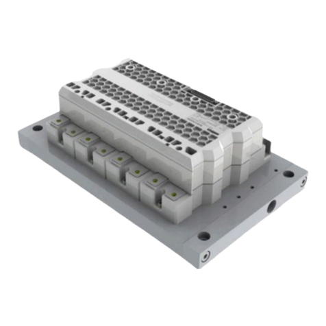
SEMIKRON SKiiP 4 User manual

© by SEMIKRON / 2017-09-07 / Technical Explanation / SKiiP
®
4
PROMGT.1023/ Rev.4/ Template Technical xplanation
Page 1/73
Please note:
Unless otherwise specified, all values in this technical explanation are typical values. Typical values are
average values derived from large quantities of tested SKiiPs and are provided for information purposes
only, thus, they’re not a binding specification. These values can and do vary under different application
conditions. All operating parameters must be validated by the user’s technical experts for each
application.
This document is valid for the following SKiiP
®
4 part numbers:
20601123 SKiiP 1814 GB12 4-3DUL 20602023 SKiiP 1814 GB12 4-3DUL
20601224 SKiiP 1814 GB17 4-3DUL 20602024 SKiiP 1814 GB17 4-3DUL
20601125 SKiiP 2414 GB12 4-4DUL 20602025 SKiiP 2414 GB12 4-4DUL
20601226 SKiiP 2414 GB17 4-4DUL 20602026 SKiiP 2414 GB17 4-4DUL
20601127 SKiiP 3614 GB12 4-6DUL 20602027 SKiiP 3614 GB12 4-6DUL
20601228 SKiiP 3614 GB17 4-6DUL 20602028 SKiiP 3614 GB17 4-6DUL
20601133 SKiiP 1814 GB12 4-3DUW 20602033 SKiiP 1814 GB12 4-3DUW
20601234 SKiiP 1814 GB17 4-3DUW 20602034 SKiiP 1814 GB17 4-3DUW
20601135 SKiiP 2414 GB12 4-4DUW 20602035 SKiiP 2414 GB12 4-4DUW
20601236 SKiiP 2414 GB17 4-4DUW 20602036 SKiiP 2414 GB17 4-4DUW
20601137 SKiiP 3614 GB12 4-6DUW 20602037 SKiiP 3614 GB12 4-6DUW
20601238 SKiiP 3614 GB17 4-6DUW 20602038 SKiiP 3614 GB17 4-6DUW
20601139 SKiiP 1814 GB12 4-3DUL 20602039 SKiiP 1814 GB12 4-3DUL
20601240 SKiiP 1814 GB17 4-3DUL 20602040 SKiiP 1814 GB17 4-3DUL
20601141 SKiiP 2414 GB12 4-4DUL 20602041 SKiiP 2414 GB12 4-4DUL
20601242 SKiiP 2414 GB17 4-4DUL 20602042 SKiiP 2414 GB17 4-4DUL
20601143 SKiiP 3614 GB12 4-6DUL 20602043 SKiiP 3614 GB12 4-6DUL
20601244 SKiiP 3614 GB17 4-6DUL 20602044 SKiiP 3614 GB17 4-6DUL
20601159 SKiiP 3614 GB12 4-6DULR 20602059 SKiiP 3614 GB12 4-6DULR
20601174 SKiiP 1814 GB12 4-3DUSL 20602074 SKiiP 1814 GB12 4-3DUSL
20601175 SKiiP 2414 GB12 4-4DUSL 20602075 SKiiP 2414 GB12 4-4DUSL
20601176 SKiiP 3614 GB12 4-6DUSL 20602076 SKiiP 3614 GB12 4-6DUSL
20601277 SKiiP 3614 GB17 4-6DULR 20602077 SKiiP 3614 GB17 4-6DULR
This technical explanation document is valid as well for customized SKiiP
®
4 with part numbers 20601xxx
and 20602xxx (SKiiPxx-Dxxxx) excepting restrictions or features which are subject of a customized
specification. The document remains effective until replaced by a subsequent revision of this document.
Technical xplanation
SKiiP
®
4
Revision: 11
Issue date: 2017-09-07
Prepared by: Marco Honsberg
Approved by: Joachim Lamp
Keyword: SKiiP4 technical explanation, Application note

© by SEMIKRON / 2017-09-07 / Technical Explanation / SKiiP
®
4
Page 2/73
Table of Contents
1.
Related documents ..................................................................................................................... 4
2.
Introduction ............................................................................................................................... 5
2.1
Heat sink ............................................................................................................................. 6
2.2
Power section ....................................................................................................................... 6
2.3
Gate Drive Unit ..................................................................................................................... 7
3.
Topologies and selection guide ..................................................................................................... 8
3.1
Type Designation Code .......................................................................................................... 8
3.2
Overview of the available types and current ratings ................................................................... 9
4.
Standards and qualification tests ................................................................................................ 10
4.1
Tests for qualification and re-qualification............................................................................... 10
4.2
lectromagnetic compatibility ( MC) ...................................................................................... 10
4.3
Isolation coordination .......................................................................................................... 11
4.4
Installation altitude ............................................................................................................. 11
5.
Gate Driver Board..................................................................................................................... 15
5.1
Overview ............................................................................................................................ 15
5.2
Gate driver interface “SKiFace” ............................................................................................. 16
5.2.1
Overview ..................................................................................................................... 16
5.2.2
Pin description .............................................................................................................. 17
5.2.3
xternal Power Supply ................................................................................................... 20
5.2.4
Switching Signal Inputs ................................................................................................. 21
5.2.5
Analogue Output Signals ................................................................................................ 22
5.2.6
HALT Logic Signal ......................................................................................................... 24
5.2.7
CMN_GPIO1 signal ........................................................................................................ 26
5.2.8
CANbus interface .......................................................................................................... 27
5.2.9
Ground connection ........................................................................................................ 29
5.2.10
Shield and protective earth/chassis connection ................................................................. 29
5.2.11
Reserved or not used signals .......................................................................................... 30
5.3
Gate driver board ................................................................................................................ 31
5.3.1
Overview ..................................................................................................................... 31
5.3.2
Digital signal transmission .............................................................................................. 31
5.3.3
Power-On-Reset ............................................................................................................ 31
5.3.4
Interlock Dead Time Generation ...................................................................................... 32
5.3.5
Short pulse suppression ................................................................................................. 32
5.3.6
IntelliOff ...................................................................................................................... 33
5.3.7
rror Management ........................................................................................................ 35
5.3.8
Analogue signals / sensor functionality ............................................................................ 38
6.
Power terminals ....................................................................................................................... 46
6.1
lectrical limits.................................................................................................................... 46
6.2
Mechanical constraints ......................................................................................................... 46
6.3
Torque at terminal connections ............................................................................................. 46
7.
Application hints ....................................................................................................................... 49
7.1
Verification of design ........................................................................................................... 49
7.2
Safe Operating Area for SKiiP
®
4 ............................................................................................ 49
7.3
Maximum blocking voltage and snubber capacitors .................................................................. 50
7.4
Definition of Thermal Resistance ........................................................................................... 50
7.5
Cooling and coolant circuit .................................................................................................... 51
7.5.1
Materials used and fluid composition ............................................................................... 51
7.5.2
Water connection description of water-cooled SKiiP
®
4 ....................................................... 53
7.6
Isolation voltage test (IVT) ................................................................................................... 55
7.7
FRT (Fault Ride Through) - Function ...................................................................................... 56
7.8
Solar function ..................................................................................................................... 59
7.9
Recommended temperature rating ........................................................................................ 60
7.10
Switching operation and current sharing between paralleled half bridge modules ........................ 63
7.11
Paralleling of SKiiP
®
4 ........................................................................................................... 63

© by SEMIKRON / 2017-09-07 / Technical Explanation / SKiiP
®
4
Page 3/73
7.12
Prevention of condensation ................................................................................................... 65
8.
Logistics .................................................................................................................................. 66
8.1
Label ................................................................................................................................. 66
8.1.1
System Label ................................................................................................................ 66
8.1.2
Half bridge Laser Label .................................................................................................. 67
8.1.3
Warranty Label ............................................................................................................. 67
8.1.4
Data Matrix Code .......................................................................................................... 67
8.1.5
Provisions and handling after use .................................................................................... 68
9.
Abbreviations ........................................................................................................................... 71
10.
Symbols .................................................................................................................................. 72

© by SEMIKRON / 2017-09-07 / Technical Explanation / SKiiP
®
4
Page 4/73
1. Related docu ents
•Data sheets SKiiP
®
4
•Diagnostic Interface SKiiP
®
4 – CANopen User Manual
•Diagnostic Interface SKiiP
®
4 – CANopen Object Dictionary
•Technical xplanation SKiiP
®
4 Parallel Board
•Technical xplanation SKiiP
®
4 F-Option
•Technical xplanation SKiFace Adapter Board
All these documents can be found on the S MIKRON internet page (www.semikron.com) or requested at
S MIKRON

© by SEMIKRON / 2017-09-07 / Technical Explanation / SKiiP
®
4
Page 5/73
2. Introduction
The 4
th
generation SKiiP “SKiiP
®
4” is an Intelligent Power Module (IPM) with highest power density and
reliability. S MIKRON’s SKiiP stands for “S MIKRON intelligent integrated Power” indicating that three
components are integrated into one IPM:
•heat sink
•power stage
•gate drive and protection circuitry
Figure 2. 1: SKiiP
®
4 – 4 fold
The power section consists of 3, 4 or 6 parallel connected half bridge modules whereas a half bridge is
defined in Figure 2.2.. The exploded assembly view of a half bridge module is shown in Figure 2.3. and as
convention the IGBT and the diode connected between DC+ and AC are named TOP IGBT and TOP diode
respectively. Consequently, the IGBT and the diode between AC and DC- are named BOT IGBT and BOT
diode respectively.
Figure 2.2: Half bridge definition

© by SEMIKRON / 2017-09-07 / Technical Explanation / SKiiP
®
4
Page 6/73
In this document following synonyms will be used for a power section with
•3 half bridge modules in parallel = 3-fold
•4 half bridge modules in parallel = 4-fold
•6 half bridge modules in parallel = 6-fold
Figure 2.3: Half bridge “exploded asse bly view”
2.1 Heat sink
S MIKRON offers highly efficient water cooled heat sinks and air cooled aluminum heat sinks. Detailed
technical parameter are given in the datasheet of the corresponding SKiiP. Customer specific heat sinks can
be designed, simulated, measured and assembled on request as well. Suitable design rules should be
followed to create such a custom specific. Please refer to the PI 12-034 for such detailed information and
get in touch with your local S MIKRON representative in case further assistance is required.
2.2 Power section
The SKiiP
®
4 power section is constructed utilizing pressure contact technology and without a copper base
plate, e.g. the SKiiP
®
4 is a “baseplateless” module. Thus, the pressure to attach the substrate to the
heatsink is homogenously induced by a dedicated pressure part on top, which is screwed to the heat sink.
The pressure contact technology facilitates that the Al
2
O
3
or AlN DCB (direct copper bonded) substrate is
pressed directly onto the heat sink without the use of a base plate and only a well defined minimum
amount of thermal compound is required. Contact springs are used for all auxiliary signal connections
between the substrate and the Gate Driver PCB like gates, auxiliary emitters and temperature sensor.

© by SEMIKRON / 2017-09-07 / Technical Explanation / SKiiP
®
4
Page 7/73
These spring contacts allow solder-free connection of the driver PCB. The pressure system ensures that the
pressure is evenly applied to the numerous contacts situated next the chips, thus, resulting in a very low
thermal and Ohmic resistance R
CC’+ ’
(refer to Figure 2.4).
Figure 2.4: Main ter inals construction principle
In the SKiiP 4 in contrast to previous generations of SKiiPs the bare chips are sintered and not soldered.
The sophisticated sintering process is based on a pulverized silver which creates a robust material
connection when suitable pressure and temperature is applied during the formation process. This sintering
process connects the chip and DCB surface extremely stably up to the melting point of silver which is as
high as 962°C.
Contact springs as mentioned before are used for all connections between substrate and Gate Driver PCB
like for the gate, auxiliary emitter and temperature sensor. These spring contacts allow the solder-free
connection of the driver board.
2.3 Gate Drive Unit
The Gate Driver Unit controls the behavior of the SKiiP under normal and exceptional operation. It receives,
checks and conditions the input signals to further transform them into suitable output signals to control the
gates of the employed IGBT. Furthermore the Gate Drive Unit establishes a safe signal insulation between
high and low voltage sides of the driver board. Additionally the gate drive circuit ensures a proper handling
of fault conditions as well as turning-off the IGBT safely even under exceptional conditions like short circuit
etc. The SKiiP 4 employs various user accessible parameter to configure and customize certain parameter
like threshold values through the integrated CANbus interface. Among those functions is an error storage,
too providing extended information as required for a detailed failure analysis.
+DC
-
DC
AC

© by SEMIKRON / 2017-09-07 / Technical Explanation / SKiiP
®
4
Page 8/73
3. Topologies and selection guide
3.1 Type Designation Code

© by SEMIKRON / 2017-09-07 / Technical Explanation / SKiiP
®
4
Page 9/73
3.2 Overview of the available types and current ratings
Table 3—1: SKiiP
®
4 standard product range and corresponding current ratings (I
Cnom
).
Table 3—1: SKiiP
®
4 standard product range
3-fold 4-fold 6-fold
SKiiP
1814GB12 4-
3DUW
SKiiP
1814GB17 4
-3DUW
SKiiP
2414GB12 4-
4DUW
SKiiP
2414GB17 4-
4DUW
SKiiP
3614GB12 4-
6DUW
SKiiP
3614GB17 4-
6DUW
SKiiP
1814GB12 4-
3DUL
SKiiP
1814GB17 4
-3DUL
SKiiP
2414GB12 4-
4DUL
SKiiP
2414GB17 4-
4DUL
SKiiP
3614GB12 4-
6DUL
SKiiP
3614GB17 4-
6DUL
I
Cnom
= 1800A I
Cnom
= 2400A I
Cnom
= 3600A

© by SEMIKRON / 2017-09-07 / Technical Explanation / SKiiP
®
4
Page 10/73
4. Standards and qualification tests
4.1 Tests for qualification and re-qualification
Table 4—1: SKiiP
®
4 Tests for qualification and re-qualification
No Test Test Conditions Standard
01 High Temperature Reverse
Bias
1000h, V
G
= 0V, 95% V
C max
T
s
=T
jmax
-10°C
I C 60747-9
02 High Temperature Gate
Stress
1000h, +/- V
G max
, T
jmax
I C 60747-9
03 High Humidity High
Temperature Reverse Bias
1000h, 85°C, 85% RH, V
C
max.
=1360 V,
V
G
=0V
I C 60068 Part 2-67
04 High Temperature Storage 1000h, T
a
= +125°C I C 60068 Part 2-2
05 Low Temperature Storage 1000h, T
a
= -40°C I C 60068 Part 2-1
06 Thermal Cycling 100 cycles, -40°C/ +125°C I C 60068 Part 2-14
07 Power Cycling ( OL-Test) 60.000 load cycles @ ∆T
j
= 110K, T
jm
=95°C
200.000 load cycles @ ∆T
j
= 70K, T
jm
=115°C
I C 60747-9
08 Vibration (Halt Test) Sinusoidal Sweep, 5g, x, y, z – axis, 2h/ axis I C 60068 Part 2-6
09 Shock (Halt Test) Half-sinusoidal Pulse, 30g, +/- x, +/- y, +/- z
direction, 1000 times per direction
I C 60068 Part 2-27
10 Corrosive gas test T
a
= 25°C, 75%RH, 4 components: H
2
S
(hydrosulphide), NO
2
(nitrogen dioxide), Cl
2
(Chlorine), SO
2
(Sulphur dioxide), 21 days
I C 60068 Part 2-60
4.2 Electro agnetic co patibility (EMC)
The SKiiP
®
4 is designed to withstand the following immunity tests with MC compliant installation:
Table 4—2: SKiiP
®
4 Electro agnetic co patibility
Immunity test Conditions Test level
Fast transients (Burst) (61000-4-4) On driver board interfaces 4kV / 5kHz
Radio Frequency Fields (61000-4-3) Polarisation: vertical + horizontal
Frequency: 80 MHz - 1000 MHz
Modulation: 80% AM, 1kHz
Far field, homogeneous
Stripline acc.11425-5 level III/F3
20V/m
200V/m
RF Conducted Disturbance (61000-4-6) Frequency: 150 kHz - 80 MHz
Modulation: 80 % AM, 1kHz
Voltage: 20V MF
Magnet field (61000-4-8) Far field, homogeneous 170A/m
lectrostatic discharge ( SD)
N 61000-4-2
Contact discharge
Air discharge
6kV
8kV

© by SEMIKRON / 2017-09-07 / Technical Explanation / SKiiP
®
4
Page 11/73
4.3 Isolation coordination
The isolation of the SKiiP
®
4 is designed according to N50178 and N61800-5-1. For working conditions
please refer to the datasheet SKiiP
®
4. 20601xxx and 20602xxx
Table 4—3: Isolation li its SKiiP
®
4
Isolation / Test level Min value
Creepage primary - secondary 14mm
Creepage secondary – heat sink potential 8mm
Clearance primary – secondary 14mm
Clearance secondary – heat sink potential 8mm
Partial discharge extinction voltage
(I C60664-1) between primary and secondary
side of driver board
1900V rms; Q
PD
< 10pC
Rated surge withstand voltage (I C60664-1)
primary to secondary
primary to heat sink
Part.Nr: 20601xxx
8kV
8kV
Part.Nr: 20602xxx
12kV
8kV
4.4 Installation altitude
Isolation coordination for SKiiP
®
4 is designed for overvoltage category III and for altitudes of up to 2000m.
The required clearance distances between mains-circuits and their environment for overvoltage category III
are listed in N50178.
For an earthed-neutral system the rated isolation voltage is defined in chapter 5.2.16.1 of N50178 as:
“…the peak value of the rated voltage between phase and earthed neutral point.”
Based on this standard sentence the rated isolation voltage in case of a grounded delta grid (Figure 4.1)
and a star grounded grid (Figure 4.2) can be derived as:
Rated isolation voltage in case of 690V grounded delta grid: 690V
Rated isolation voltage in case of 690V star grounded grid: 400V
Figure 4.1: Grounded delta grid Figure 4.2: Star grounded circuit network (690V-
TN-grid)
Based on the type of grid and the voltage level the required clearance distance for basic and reinforced
isolation can differ from the designed ones.
According to HD625 S1 and I C60664-1 the maximum altitude can be calculated based on the factors
between required and designed clearance distances.
L
1
L
2
L
3
U
L
1
3
U
L
1
2
U
L23
690V
L
1
L
3
L
2
U
L1
U
L2
U
L3
U
LL
=690V
U
LE
=400V

© by SEMIKRON / 2017-09-07 / Technical Explanation / SKiiP
®
4
Page 12/73
Table 4—4: Altitude correction factors (IEC 60664-1)
Altitude Normal barometric
pressure
Multiplication factor
for clearances
m kPa
2 000 80,0 1,00
3 000 70,0 1,14
4 000 62,0 1,29
5 000 54,0 1,48
6 000 47,0 1,70
7 000 41,0 1,95
8 000 35,5 2,25
9 000 30,5 2,62
10 000 26,5 3,02
15 000 12,0 6,67
20 000 5,5 14,5
The overvoltage category influences the installation altitude, too. In order to increase the installation
altitude further the overvoltage category needs to be reduced ( N50178):
“As an alternative to the values of table 3, columns 2 to 5 (of the cited standard), the clearance between
mains-circuits of an EE and its environment may be designed in accordance with overvoltage category , if
facilities are provided which reduced overvoltages of category to values of category …However for
reinforced isolation according to column 7 (of the cited standard) shall not be reduced.”
The required clearance distances between mains-circuits and their environment for overvoltage category II
are listed in N50178.
If safety isolation is necessary the maximum altitude of SKiiP
®
4 is 6250 m (690 TN grid and overvoltage
category II).
If only basic isolation is required even higher operation altitudes are possible. In case of a 690V TN grid
and overvoltage category II an altitude of theoretically 9000 m for SKiiP
®
4 is possible.
This is the case when an additional basic isolation is implemented between the SKiiP 4 driver interface and
controller board. This can be realized by the following means:
•Use of fiber optic for control signals (TOP, BOT, rror) and
•SKiiP analogue signals (current, DC-voltage and temperature measurement) are not used and
•all SKiiPs are supplied by separate power supplies to which no other circuit is connected.
The above described implementation is shown in Figure 4.3. The “F-Option board” for an optical fibre
based isolation of the SKiiP
®
4 (please refer to Figure 4.3) can be ordered separately and can be easily
mounted on the SKiiP
®
4 top cover.

© by SEMIKRON / 2017-09-07 / Technical Explanation / SKiiP
®
4
Page 13/73
Figure 4.3: I ple entation of additional basic isolation between SKiiP
®
4 driver interface and
controller board
Finally, the installation altitude of the SKiiP 4 depends on:
•Grid configuration (star grounded grid, delta grounded grid)
•The voltage level of the line to earth voltage (rated isolation voltage)
•The overvoltage category (II or III)
•Whether safety isolation is required or not

© by SEMIKRON / 2017-09-07 / Technical Explanation / SKiiP
®
4
Page 14/73
Table 4—5 summarizes the installation altitudes for SKiiP
®
4.
Table 4—5: Installation altitudes for SKiiP
®
4 as function of the grid configuration, overvoltage
category and required isolation degree
SKiiP4
(with 690V
grounded delta)
Overvoltage category III Overvoltage category II
Grounded delta
grid TN 690V Grounded delta
grid TN 690V
Basic
isolation
against
ground
Required
for
2000m
8 mm 5,5 mm 5,5 mm 3 mm
xisting 8 mm
Factor 1 1,45 1,45 2,66
Altitude 2000 4840 4840 9000
Rein-
forced
isolation
Required
for
2000m
14 mm 8 mm 14mm 8mm
xisting 14 mm
Factor 1 1,75 1 1,75
Altitude 2000 6250 2000 6250
Maxi u Altitude
with safety
isolation
2000 4840 2000 6250
Maxi u Altitude
without safety
isolation
2000 4840 4840 9000
L
1
L
2
L
3
U
L
1
3
U
L
1
2
U
L23
690V
L
1
L
3
L
2
U
L1
U
L2
U
L3
U
LL
=690V
U
LE
=400V
L
1
L
2
L
3
U
L
1
3
U
L
1
2
U
L23
690V
L
1
L
3
L
2
U
L1
U
L2
U
L3
U
LL
=690V
U
LE
=400V

© by SEMIKRON / 2017-09-07 / Technical Explanation / SKiiP
®
4
Page 15/73
5. Gate Driver Board
5.1 Overview
The functionality of the Gate Driver board is indicated in the following block diagram.
•Gate driver interface SKiFace marked as red block in Figure 5.1 (refer to Chapter 5.2)
•Gate driver board, marked as green block in Figure 5.1 (refer to Chapter 5.3)
Figure 5.1: Gate Driver Board block diagra

© by SEMIKRON / 2017-09-07 / Technical Explanation / SKiiP
®
4
Page 16/73
5.2 Gate driver interface “SKiFace”
5.2.1 Overview
The Gate Driver Interface “SKiFace” is shown in the red colour marked frame of Figure 5.2. “SKiFace
defines the 25 pin D-Sub male plug connector and the corresponding signal assignment. The appearance of
the plug, its pin-out and dimensions are summarized in Figure 5.3.
The SKiFace interface provides pins for:
•xternal Power Supply
(refer to chapter 5.2.3)
•Switching signal input
(refer to chapter 5.2.4)
•Analogue signals (refer to chapter 5.2.5)
•HALT logic (refer to chapter 5.2.6)
•CMN_GPIO 1 output (refer to chapter 5.2.7)
•CMN_GPIO 2 (refer to chapter 5.3.6)
•CAN interface (refer to chapter 5.2.8)
Figure 5.2: Gate Driver Interface
Figure 5.3: SKiiP
®
4 - connector D-Sub 25 pin, ale plug, vertical, top view
Picture Pin Configuration Dimensions
When connecting the SKiiP
®
4 to a control circuit the following recommendations shall be observed for a
proper cable selection:
•Cable length should be kept shorter than 3m
•Utilization of shielded cables is recommended
•Longer cables must be shielded

© by SEMIKRON / 2017-09-07 / Technical Explanation / SKiiP
®
4
Page 17/73
A verification of mechanical stability and MC behaviour under customer’s application conditions is
necessary.
As the SKiFace interface is a standardized, it is also used in other S MIKRON products. Due to that not all
signals are used for SKiiP
®
4.
An unused signal is: HB_RSRVD
Please note: The protective plastic cover of the D-Sub connector should be removed only just before
the start of operation ( SD-Handling and protection)
5.2.2 Pin description
Table 5—1: Pin configuration SKiiP
®
4
PIN Signal Function Specification
1/2/3 PWR_VS Power Supply +24V (+/- 20%)
4 CMN_GPIO2
Digital input/ output
Bidirectional status
signal
Sync-signal for parallel operation (available
after activation through CAN-bus message)
For details see IntelliOff function, p. 33
5 CMN_HALT
Digital input/ output
Bidirectional status
signal
LOW (dominant) = not ready to operate (e.g.
error) HIGH (recessive) = ready to operate
For details refer to HALT Logic Signal, p. 24
6 CMN_T MP Temperature signal out
This pin is used to indicate the temperature
sensor’s analogue signal.
Max output current: 5mA
Nominal voltage range: 0 … +10V
Refer to Integrated DCB-Temperature Sensor,
p. 42
7 CMN_DCL DC-Link voltage out
This pin is used to indicate the DC-Link voltage
level.
Max. output current: 5mA
Nominal voltage range: 0 … +10V
For details refer to DC-Link-Voltage Sensing, p.
43
8 HB_TOP Switching signal input
for high side IGBT
LOW = High side IGBT off
HIGH = High side IGBT on
For details refer to Switching Signal Inputs, p.
21
9 HB_RSRVD Reserved Not connected
10 HB_I Current sensor out
This pin is used to indicate the current sensor’s
analogue signal.
Max. output current: 5mA
Nominal voltage range: -10V … +10V
For details refer to AC-current sensor, p. 38
11 CAN_H CAN interface INPUT/
OUTPUT HIGH
Input impedance = very high
Specification according to ISO 11898.
12 CAN_H Internally connected to pin 11
13 SHLD_GND GND Internally connected to PWR_GND
14/15/1
6 PWR_GND Ground for PWR_VS

© by SEMIKRON / 2017-09-07 / Technical Explanation / SKiiP
®
4
Page 18/73
17 CMN_GND Ground for CMN_HALT,
CMN_GPIO1/2 Internally connected to PWR_GND
18 CMN_GPIO1 Digital Input/Output
General purpose IO
Inverted CMN_HALT signal (except in case of
an activated FRT-function, please refer to
chapter CMN_GPIO1 signal, p. 26
19 CMN_T MP_GND Ground for CMN_T MP
20 CMN_DCL_GND Ground for CMN_DCL
21 HB_BOT Switching signal input
for low side IGBT
LOW = Low side IGBT off
HIGH = Low side IGBT on
For details refer to Switching Signal Inputs,
p.21
22 HB_GND
Ground for
CMN_HB_TOP,
CMN_HB_BOT,
CMN_HB_RSRVD
Internally connected to PWR_GND
23 HB_I_GND Ground for HB_I
24 CAN_L CAN interface INPUT/
OUTPUT LOW
Input impedance = very high;
Specification according to ISO 11898.
25 CAN_L Internally connected to pin 24

© by SEMIKRON / 2017-09-07 / Technical Explanation / SKiiP
®
4
Page 19/73
Figure 5.4: Overview sche atics SKiFace interface (CMN_GPIO1/2 and CMN_HALT are not
shown
CMN_TEMP = DCB-sensor temperature
CMN_DCL = DC-Link voltage
CMN_TEMP_GND = Analogue ground
CMN_DCL_GND = Analogue ground
B_I = AC current signal
B_I_GND = Analogue ground
B_TOP = Switching signal TOP
B_BOT = Switching signal BOT
Chassis / PE
14-17, 22
1, 2, 3
6
19
7
20
23
10
8
21
SKiiP®4 Driver interface
SKiFace
Controller interface
GND
Analogue output
Digital input
Digital output
Digital output
GND
GND
GND
GND
Analogue input
VS
PWR_GND
CMN_GND
B_GND
PWR_VS= Supply voltage
GND
DC
DC
S LD_GND
13
D-Sub cable shield
Capacitive
g ounding
di ect
g ounding
24V0V
Exte nal powe supply
RXD
TXD
CAN_H
CAN_L
RXD
TXD
CAN_H
CAN_L
11
24
VS
VSVS
GND
Analogue input
GND
Analogue input
Analogue output
Analogue output
VS
Digital input
GND
VS
CAN_
25
12
CAN_
CAN_L
CAN_L

© by SEMIKRON / 2017-09-07 / Technical Explanation / SKiiP
®
4
Page 20/73
The left side shows the equivalent circuit diagram of the driver board with ground connections. The right
side shows an application example of the controller side.
5.2.3 External Power Supply
Table 5—2 shows the required features of an appropriate external power supply for a SKiiP
®
4.
Table 5—2: Require ents to the auxiliary power supply
Power supply
The maximum ratings for the supply voltage are given in the
SKiiP
®
4 data sheet on page 1 (refer to symbol Vs). The
supply voltage is defined at the SKiiP
®
4 input, not at the
controller output (voltage drop on connection cable)
Maximum rise time of 24V <2 s
Rated current 1,5 times of the maximum driver input current
Minimum peak current 2 times of the maximum driver input current
(At least 1,5A)
Please note: Do not apply switching signals during power up.
The external power supply requires the capability to feed a minimum inrush current into the SKiiP 4 at
start-up of the system without entering a fault state itself. Typically power supplies with fold-back
characteristic or hiccup-mode can create problems if insufficient over current margin is available. The
voltage has to rise continuously and without any plateau formation.
In order to ensure continuous operation and to have sufficient margin in case of overload it is
recommended to select the rated current of the external power supply sufficiently higher than the SKiiP’s
maximum specified input current (see symbol Is on page 2 of the corresponding SKiiP
®
4 datasheet).
If the power supply is able to provide a higher current, a peak current will flow in the first instant to mainly
charge the input capacitances on the driver. The peak current value will be limited only by the external
power supply and the effective impedances (e.g. cabling etc-) as present in the connection between power
supply and the SKiiP. It is recommended to avoid the paralleling of several customer side external power
supply units. Their different current limitations may lead to drops in the supply voltage and unpredictable
instable behaviour.
The formula given in the SKiiP
®
4 datasheet for calculating the supply current I
S
(page 2) consists of three
parts:
•The first part is the current consumption of the driver during standby. No switching signals are
applied. Consequently, no AC-current is flowing. The example below is given for a
SKiiP2414GB17 4 (I
SO
=260mA).
•The second part is the required current consumption of the driver during switching.
•The third part is the current consumption required by the integrated current sensor to compensate
the present value of the AC-current.
2
21
260
ACsws
IkfkmAI ⋅+⋅+=
Current
consumption of integrated current sensor
Current consumption of
driver during switching
Standby current consumption of the
driver
This manual suits for next models
63
Table of contents
Other SEMIKRON Control Unit manuals
Popular Control Unit manuals by other brands
Digi
Digi ConnectCore 8X Hardware reference manual

schmersal
schmersal SRB 401EM-115V operating instructions

Macnaught
Macnaught OCVSF-001 instruction manual
Bosch
Bosch Rexroth IndraControl XFE 01.1 Series operating instructions
HESCH
HESCH HIMOD HE 5820 DI Operation manual

Civacon
Civacon NV4000 Installation & maintenance manual
