Sharp DV-SL800W User manual

DV-SL800W
1
DVD PLAYER
Page
SAFETY PRECAUTION FOR SERVICE MANUAL ...............................................................................................................2
AC POWER SUPPLY CORD.................................................................................................................................................2
SPECIFICATIONS..................................................................................................................................................................3
LASER BEAM SAFETY PRECAUTIONS ..............................................................................................................................4
STANDARD NOTES FOR SERVICING.................................................................................................................................5
OPERATING CONTROLS AND FUNCTIONS.......................................................................................................................8
BLOCK DIAGRAMS..............................................................................................................................................................10
SCHEMATIC DIAGRAMS.....................................................................................................................................................12
IC’S PIN VOLTAGE CHART..................................................................................................................................................26
WAVEFORMS.......................................................................................................................................................................29
OVERALL WIRING CONNECTION......................................................................................................................................32
WIRING DIAGRAM...............................................................................................................................................................34
NOTES ON SCHEMATIC DIAGRAM/TYPES OF TRANSISTOR AND LED........................................................................44
TROUBLESHOOTING..........................................................................................................................................................45
IC PIN FUNCTION DESCRIPTIONS....................................................................................................................................46
FL DISPLAY..........................................................................................................................................................................74
PARTS GUIDE/EXPLODED VIEW
SERVICE MANUAL
No.S9504DVSL800W
CONTENTS
This document has been published to be used for
after sales service only.
The contents are subject to change without notice.
DV-SL800W
MODEL
• In the interests of user-safety (Required by safety regula-
tions in some countries) the set should be restored to its
original condition and only parts identical to those specified
be used.
REMOTE
SENSOR
PLA
Y
– SKIP –
STOP
POWER
OFF ON
OPEN/CLOSE
DVD PLA
YER DV-SL8
12
MIC
VOL
D
SVCD
PBC
ALL
5
46
OPEN/
CLOSE
SETUP
OSDSTEPSOUND
DIGESTSLOWMUTE
PAL/NTSC
RANDOM
AUDIO PROG
VOLUME
SUBTITLE
ANGLE
I/PSCAN
RESUME
DIRECT
TITLE
MENU/PBC
A-B
REPEAT
ZOOM
E
C
H
O
(–)
E
C
H
O
(+)
DVDVIDEOPLAYER
92LWIR2491-D71
3
2
1
789
0
ENTER
SCOREON/OFF
Parts marked with " " are important for maintaining the safety of the set. Be sure to replace these
parts with specified ones for maintaining the safety and performance of the set.

DV-SL800W
2
SAFETY PRECAUTION FOR SERVICE MANUAL
lThis product is classified as a CLASS 1 LASER PRODUCT.
lWARNINGS:
The AEL (Accessible Emission Level) of Laser Power Output for this model is specified to be lower than Class 1
Requirements. However, the following precautions must be observed during servicing to protect your eyes against
exposure to the Laser beam.
(1)When the cabinet has been removed, the power is turned on without a compact disc, and the Pickup is on a
position outer than the lead-in position, the Laser will light for several seconds to detect a disc. Do not look into
the Pickup Lens.
(2)The Laser Power Output of the Pickup inside the unit and replacement service parts have already been adjusted
prior to shipping.
(3)No adjustment to the Laser Power should be attempted when replacing or servicing the Pickup.
(4)Under no circumstances look directly into the Pickup Lens at any time.
(5)CAUTION - Use of controls or adjustments, or performance of procedures other than those specified herein may
result in hazardous radiation exposure.
AC POWER SUPPLY CORD
92LCCP01000430
92LVPE00327911
92LVPE41A25310

DV-SL800W
3
SPECIFICATIONS
lGeneral
lDVD player
As part of our policy of continuous improvement, SHARP reserves the right to make design and specification changes
for product improvement without prior notice. The performance specification figures indicated are nominal values of
production units. There may be some deviations from these values in individual units.
Power source AC 110~240 V, 50/60 Hz
Power consumption Power on:12W
Dimensions Width: 430 mm (16-15/16”)
Height: 37 mm (1-1/2”)
Depth: 200 mm (7-7/8”)
Weight 1.70 kg (3.75 lbs.)
Audio input terminals MIC x 2 (ø6.3)
Audio output terminals Analogue output (OUT): RCA type × 1 pair (L/R)
Video output terminals S-video output: S-terminal × 1,Component video output: (Y, PB, PR)
Video output: RCA type × 1
Digital output terminals COAXIAL
Signal system PAL/NTSC colour
Supported disc types DVD (with the same region number on the back of the unit), SVCD, VCD, audio CD, CD-R,
CD-RW, MP3, JPEG
Video signal Horizontal resolution: 500 lines
S/N ratio: 70 dB
Audio signal Frequency characteristics Linear PCM DVD: 20 Hz to 20 kHz
(sampling rate: 48 kHz)
20 Hz to 20 kHz
(sampling rate: 96 kHz)
CD: 20 Hz to 20 kHz
S/N ratio CD: 94 dB (1 kHz)
Dynamic range Linear PCM DVD: 95 dB
CD: 94 dB
Total harmonic distortion ratio 0.01 % maximum

DV-SL800W
4
LASER BEAM SAFETY PRECAUTIONS
This DVD player uses a pickup that emits a laser beam.
The laser beam is emitted from the location shown in the figure. When checking the laser diode, be sure to keep your eyes at least
30cm away from the pickup lens when the diode is turned on. Do not look directly at the laser beam.
Caution: Use of controls and adjustments, or doing procedures other than those specified herein, may result in hazardous radiation
exposure.
Do not look directly at the laser beam coming
from the pickup or allow it to strike against
your skin.
Drive Mecha Assembly
Laser Beam Radiation
Laser Pickup
Turntable

DV-SL800W
5
STANDARD NOTES FOR SERVICING
How to Remove / Install Flat Pack-IC
1. Removal
With Hot-Air Flat Pack-IC Desoldering Machine:
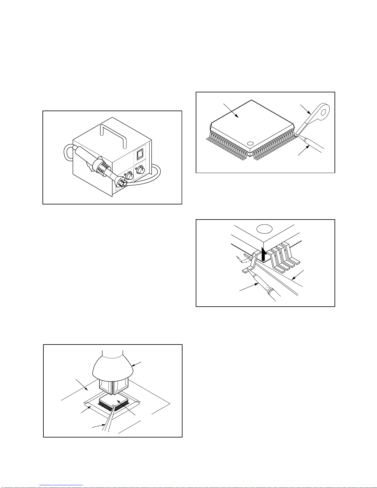
(1) Prepare the hot-air flat pack-IC desoldering ma-
chine, then apply hot air to the Flat Pack-IC (about 5
to 6 seconds). (Fig. S-1-1)
Fig. S-1-1
(2) Remove the flat pack-IC with tweezers while apply-
ing the hot air.
(3) Bottom of the flat pack-IC is fixed with glue to the
CBA; when removing entire flat pack-IC, first apply
soldering iron to centre of the flat pack-IC and heat
up. Then remove (glue will be melted). (Fig. S-1-6)
(4) Release the flat pack-IC from the CBA using twee-
zers. (Fig. S-1-6)
Caution:
1. Do not supply hot air to the chip parts around the flat
pack-IC for over 6 seconds because damage to the
chip parts may occur. Put masking tape around the
flat pack-IC to protect other parts from damage.
(Fig. S-1-2)
2. The flat pack-IC on the CBA is affixed with glue, so
be careful not to break or damage the foil of each pin
or the solder lands under the IC when removing it.
Hot-air
Flat Pack-IC
Desoldering
Machine
CBA
Flat Pack-IC
Tweezers
Masking
Tape
Fig. S-1-2
With Soldering Iron:
(1) Using desoldering braid, remove the solder from all
pins of the flat pack-IC. When you use solder flux
which is applied to all pins of the flat pack-IC, you can
remove it easily. (Fig. S-1-3)
Flat Pack-IC Desoldering Braid
Soldering Iron
Fig. S-1-3
(2) Lift each lead of the flat pack-IC upward one by one,
using a sharp pin or wire to which solder will not
adhere (iron wire). When heating the pins, use a fine
tip soldering iron or a hot air desoldering machine.
(Fig. S-1-4)
Fine Tip
Soldering Iron
Sharp
Pin
Fig. S-1-4
(3) Bottom of the flat pack-IC is fixed with glue to the
CBA; when removing entire flat pack-IC, first apply
soldering iron to centre of the flat pack-IC and heat
up. Then remove (glue will be melted). (Fig. S-1-6)
(4) Release the flat pack-IC from the CBA using twee-
zers. (Fig. S-1-6)
With Iron Wire:
(1) Using desoldering braid, remove the solder from all
pins of the flat pack-IC. When you use solder flux
which is applied to all pins of the flat pack-IC, you can
remove it easily. (Fig. S-1-3)
(2) Affix the wire to a workbench or solid mounting point,
as shown in Fig. S-1-5.
(3) While heating the pins using a fine tip soldering iron
or hot air blower, pull up the wire as the solder melts
so as to lift the IC leads from the CBA contact pads
as shown in Fig. S-1-5.

DV-SL800W
6
(4) Bottom of the flat pack-IC is fixed with glue to the
CBA; when removing entire flat pack-IC, first apply
soldering iron to centre of the flat pack-IC and heat
up. Then remove (glue will be melted). (Fig. S-1-6)
(5) Release the flat pack-IC from the CBA using twee-
zers. (Fig. S-1-6)
Note:
When using a soldering iron, care must be taken to
ensure that the flat pack-IC is not being held by glue.
When the flat pack-IC is removed from the CBA,
handle it gently because it may be damaged if force
is applied.
To Solid
Mounting Point
Soldering Iron
Iron Wire
or
Hot Air Blower
Fig. S-1-5
Fine Tip
Soldeing Iron
CBA
Flat Pack-IC
Tweezers
Fig. S-1-6
2. Installation
(1) Using desoldering braid, remove the solder from the
foil of each pin of the flat pack-IC on the CBA so you
can install a replacement flat pack-IC more easily.
(2) The "●" mark on the flat pack-IC indicates pin 1. (See
Fig. S-1-7.) Be sure this mark matches the 1 on the
PCB when positioning for installation. Then presol-
der the four corners of the flat pack-IC. (See Fig. S-
1-8.)
(3) Solder all pins of the flat pack-IC. Be sure that none
of the pins have solder bridges.
Example :
Pin 1 of the Flat Pack-IC
is indicated by a " " mark. Fig. S-1-7
Presolder
CBA
Flat Pack-IC
Fig. S-1-8

DV-SL800W
7
Instructions for Handling
Semi-conductors
Electrostatic breakdown of the semi-conductors may
occur due to a potential difference caused by electrostatic
charge during unpacking or repair work.
1. Ground for Human Body
Be sure to wear a grounding band (1MΩ) that is properly
grounded to remove any static electricity that may be
charged on the body.
2. Ground for Workbench
Be sure to place a conductive sheet or copper plate with
proper grounding (1MΩ) on the workbench or other
surface, where the semi-conductors are to be placed.
Because the static electricity charge on clothing will not
escape through the body grounding band, be careful to
avoid contacting semi-conductors with your clothing.
CBA
< Incorrect >
CBA
Grounding Band
Conductive Sheet or
Copper Plate
< Correct >

DV-SL800W
8
OPERATING CONTROLS AND FUNCTIONS
nMain unit (front panel)
1. ON/STANBY Button
2. Microphone Volume Controls
3. Play or Pause Button
4. Stop Button
5. Disc Tray
6. Disc Tray Open/Close Button
7. Remote Sensor
8. Microphone Sockets
9. Chapter (track) Skip down
10. Chapter (track) Skip up
nMain unit (rear panel)
1.Component Video Output Sockets
2.Video Output Socket
3.AC Power Lead
4.Digital Output Socket (Coaxial)
5.Audio Output Sockets
6.S-Video Output Socket
9
8
7
65
123 4
10
Rating label
3
46
5
21

DV-SL800W
9
nRemote Control 1. Remote Control Transmitter
2. ON/STANDBY
3. Subtitle Select Button
4. Angle Select Button
5. Interlace and Progressive Scan
6. Direct Button
7. Setup Button
8. Title Select Button
9. Zoom Button
10. Cursor or Echo Level Up and Down Buttons
11. Key Control Button (normal)
12. Key Control Button (lower)
13. Fast Forward
14. Fast Backward
15. Step Button (Frame by frame advance Playback)
16. On screen Display On/Off Button
17. Video CD Digest Button
18. Slow Button
19. PAL/NTSC Select Button
20. Disc Tray Open/Close Button
21. Direct Number Buttons
22. Menu/Playback Control On/Off Button
23. KARAOKE Scoring ON/OFF
24. A-B Repeat Button
25. Repeat Play Button
26. Enter Button
27. Play or Pause Button
28. Key Control Button (highest)
29. Stop Button
30. Chapter (track) Skip Up
31. Chapter (track) Skip Down
32. Sound Button
33. Mute Button
34. Volume Up and Down Buttons
35. Programme Button
36. Audio Select Button
37. Random Button
546
OPEN/
CLOSE
ON/
STANDBY
SETUP
OSD STEP SOUND
DIGEST SLOW MUTE
PAL/NTSC
RANDOM
AUDIO PROG
VOLUME
TITLE
MENU/PBC
A-B
REPEAT
ZOOM
DVD VIDEO PLAYER
321
789
0
ENTER
SUBTITLE
ANGLE
I
/
P-SCAN
DIRECT
SCORE ON/OFF
E
C
H
O
(Ð)
E
C
H
O
(+)
92LWIR2491-D71
1
2
20
21
22
23
24
25
26
27
28
29
30
31
32
33
34
35
36
37
3
4
5
6
7
8
9
10
11
12
13
14
15
16
17
18
19

DV-SL800W
10
BLOCK DIAGRAM
FIGURE 1. BLOCK DIAGRAM
A
B
C
D
E
F
G
H
123456
AM5869S/F
REMOTE
SENSOR
VFD KEY*6
LM4558
CE 2752
120-240V IN
SWITCHING POWER
15W
SPHE8202S
MICMIC
VFD DRIVER
CONTROL BOARD
LOADER
DVD MAIN UNIT
MX29LV040T/B
4MB FLASH 1*16M SDRAM
EASTWIN
MPEG DECORDER
RF AMP
SEVOR
DOLBY DIGITAL 5.1
DECORDER
DOLBY PROLOGIC2
DTS DECORDER
VIDEO DECORDER
DSP
ADC
MOTOR DRIVER
V6312
ST2104
KARAOKE BOARD
MIC AMP
LM4558
L
R
2 CHANNEL(AMP)2 CHANNEL
D/A
SD0
SD1
SD2
MIC ALC
M07
1*16M SDRAM
VIDEO FILTER
COAX
S-VIDEO
CVBS
VUY

DV-SL800W
11
-MEMO-

DV-SL800W
12
SCHEMATIC DIAGRAM
POWER PCB SCHEMATIC DIAGRAM
Figure 1: POWER PCB SCHEMATIC DIAGRAM (1/2)
A
B
C
D
E
F
G
H
123456
F1
LF1
T250V/1A
CX1
R2
470K
R6
820K
R3
820K R3
100K
D5
FR107
C1
IN4007
D2 D1
D3 D4
R1
470K
0.1uF/250V
15uF/400V
C2
T1
11
10
11
12
1
1
1
2
6
6
9
7
88
7
8
44
4700PF/1KV
PCI-2
ZD3
18V
D7
IN4148
R8
560R
R10
470R R7
39K
0.001uF/100V
C4
4
2
55
2
3
C3
0.47uF/50V
CY3
3300pF/250V
CON1
Q1
03NK60
ZD1
18V R13
4.7K
R12
10K
R11
220R
R4 4.7R
R14 4.7R
R17 4.7R
R16 4.7R
C5
472/50V
R9
1K
C6
103/50V
Q5
PMBS3904
Q2
PMBS3906
!
!
!
!
!
LN
+
!
!
When servicing, pay attention as the area closed
by this line ( ) is directly connected with
AC.

DV-SL800W
13
Figure 1: POWER PCB SCHEMATIC DIAGRAM (2/2)
78 9 10 11 12
PR1007
D10
100uF/35V
C9
10 10
11
12
11
12
6
6
9
9
7
88
7
88
D16 10R/1W
R18 (JUMP)
Q4 BT169D
D12
PR1007
R27 L2 (3uH)
10R
PR105
D13
C11
330uF/16V
R36
1M
C19
2200PF/100V C13
1500uF/10V
Y
3
F
/250V
C14
470uF/10V
ZD4
6.2V/1W
R25
750R
R39
R40
C21 R30
680
PC1-1 R33
10K
R34
10.0K
U1
TL431
R31
1K C16
R32
10K 1uF/50V
104 1206
Q6
C1815
C8
47uF/16V
A1015
Q7
Q3
C1815 R23
10K
0R
R22
R21
10K
C10
10uF/63V
C7
220uF/16V
R37 (JUMP)
R38
1K
IN5822
D14
300R 300R
ZD2
5.1V
!
1
2
3
4
5
6
7
8
V+
V-
-24V
+12V
GND
+5V
PCON
S+5V

DV-SL800W
14
CONTROL PCB SCHEMATIC DIAGRAM
Figure 2: CONTROL PCB SCHEMATIC DIAGRAM (1/2)
A
B
C
D
E
F
G
H
123456
C203 104
GRID5
GRID6
SEG16/GRID7
SEG15/GRID8
SEG14/GRID9
SEG13/GRID10
VEE
SEG12/GRID11
SEG11
grid4
grid3
grid2
grid1
VDD
LED4
LED3
LED1
LED2
VSS
OSC2
SW1
SW2
SW3
SW4
DOUT
DIN
VSS
CLK
STB
1
2
3
4
5
6
7
8
9
34
35
36
37
38
39
40
41
42
43
44
33
32
31
30
29
28
27
26
25
V6312
R214
51K
R2
0
10
K
R215
561
LED
-27V
VCC
IRT
SN2
R203
10K R209
10 R210
10
C206
100UF/16V
C206
104
CN200
IR/VFD
C209
NOP
C210
NOP
C211
NOP R205 10K
R204 10K
R211 5.6K
V6312
IC2
C207
100UF/16V
2
21
1
9
8
7
6
5
4
3
2
1

DV-SL800W
15
Figure 2: CONTROL PCB SCHEMATIC DIAGRAM (2/2)
78 9 10 11 12
6
SEG13/GRID10
VEE
SEG12/GRID11
SEG11
SEG10
SEG9
SEG8
SEG7
SEG6/KS6
SEG5/KS5
SEG4/KS4
SEG3/KS3
SEG2/KS2
SEG1/KS1
VDD
KEY4
KEY3
DIN
VSS
CLK
STB
KEY1
KEY2
6
7
8
9
10
11
22
21
20
19
18
17
16
15
14
13
12
1
2
3
4
1
2
3
4
1
2
3
4
1
2
3
4
28
27
26
25
24
23
R206
10K
R207
10K
R212
10K R213
10K
CN302
CN201
CN301
CN208
D6
IN4148 D5
IN4148
RB302
RB301B
RB208 K11
D210 LED
12
RB201
LED
K10
K7
K12
K9
K8
12
12
12
12
12
VCC
VFD2
HNV-05SS48
F1
F1
NX
P16
P15
P14
P13
P12
P11
P10
P9
P8
P7
P6
P5
P4
P3
P2
P1
NX
NX
NX
NX
NX
1G
2G
3G
4G
5G
NP
F2
F2
1
2
3
4
5
6
7
8
9
10
11
12
13
14
15
16
17
18
19
20
21
22
23
24
25
26
27
28
29
30
31
32

DV-SL800W
16
KARAOKE PCB SCHEMATIC DIAGRAM
Figure 3: KARAOKE PCB SCHEMATIC DIAGRAM (1/2)
A
B
C
D
E
F
G
H
123456
5
6
84
3
21
84
11
3
2
+12V
+12V
R23
N C
R22
NC
+12V
R L IN
+
-
IC
1
LM
4
+
-
IC1
A
LM4
5
R15 220 OHM
R2 30k
R1 30k
C10
C8
470P(471PF)
+
C1
4.7U/16V
R12
R6 1K
C9
470P(471PF)
C11
R7 1K
R18
2.2K
R
7
VR2
10K
R4 100k
+C6
100U/16V
R13
47K
R14
47K
R5
100k
R3
47K
+
C2
4.7U/16V
+
C3
4.7U/16V
R10
5.6K
R11
5.6K
VR1
10k
JACK1
JACK2
R25
NC
R24
NC

DV-SL800W
17
Figure 3: KARAOKE PCB SCHEMATIC DIAGRAM (2/2)
78 9 10 11 12
6
+12V
7
1
1
2
3
4
V
+12V
VIN+
MIC LOUT
R L IN
MIC ROUT
GND
IC1B
LM4558
IC1A
LM4558
C10 221PF
R12 36K
+
C5
4.7U/16V
+
C4
4.7U/16V
+
C7 100u/16V
C11 221PF
R17
750
R20
200 OHM R16 4.7K
R9
30k R8 1K
CN1
R19
100OHM
+C12
220U/16V
C13
0.1U(104PF)
D1
1N4148
Q1
2SC945(NPN)
Q2
2SC945(NPN)
C14 1U
C15 1U
D2
1N4148
R21 0OHM
R26
NC
C16 1U

DV-SL800W
18
MAIN PCB SCHEMATIC DIAGRAM
Figure 4: MAIN PCB SCHEMATIC DIAGRAM (1/8)
Pickup head parameter Motor Driver AM5869
R155 R154 R145 R146 R53 R111 R212
D
CD_VR
LDSW
DVD_VR
CD_VR
PUH_CDLD
DVD_VR
PUH_DVDLD
CDMDI
B
CDVR
PUH_CDLD#
PUH_DVDLD#
C
A
PUHRF
E
F
DVD_VR#
DVDMDI
VREF1
PUH_DVDLD
DVDLDO
CDLDO
PUH_CDLD
C119
0.1UF
+C181
47UF16V
R154
5.1
+C180
47UF16V
+C176
100UF10V
R155
5.1
C118
0.1UF
C120
0.1UF
R146
0
R145 0
L11 10UH
C102
0.1UF
R157
100K
C101
0.1UF
R159
470
C104
0.1UF
R156 100K
C103
0.1UF
R158
470
C179 0.1U
26 25
17
16
15
14
13
12
11
10
9
8
7
6
5
4
3
2
1
18
19
20
21
22
23
24
27 28
CN101
ELCO-CON24(Left)
R144 0
C107
0.1UF
R143 0
C106
0.1UF
C1
0
0.1
U
C178
0.1U
C105
0.1UF
C177 0.1U
TP4
FOC-
TP3
FOC+
TP2
RAD-
L12 10UH
TP1
RAD+
GND
GND
RF+5V
GND
GND
RF+5V
GND
DVCC33 VCC1.8
RF+5V
GND GND
GND
RF3.3V
GND
RF3.3V
BOTTOM CONTACT
CLOSE TO CONNECTOR!
5.1
4.7
00 1000P2.2K
20K
SAS8801W
4.7 100
33K
Sony 100
5.1
1500P12K
M07C
Mitsumi
5.1
5.1
5.1
5.1
0
0
0
0
2.2K
2.2K
12K
12K
1500P
1500P
FOC-
FOC+
RAD+
RAD-
FOC+
FCO
FOC-
VOFC+ 14
VOFC- 13
TRB1
2
VINFC
1
BIAS
25K
+
-
10K
Driver(6 x)
+
-
IC105
AM5869S
DIP28-SSOPH
TRB1
Q105
3904
G
DS
Q103
2SK3018
G
DS
Q104
2SK3018
GND
Q101
2SB1132
Q102
2SB1132
D102
1N4148
D101
1N4148
A
B
C
D
E
F
G
H
123456

DV-SL800W
19
MAIN PCB SCHEMATIC DIAGRAM
Figure 4: MAIN PCB SCHEMATIC DIAGRAM (2/8)
AU_XCK
AU_BCK
RA16
RA18
SPDIF_OUT
AU_D0
AU_D1
AU_D2
AU_LRCK
AUDIO_MUTE
RFI
RFO
CVBS1
B/U
G/Y
R/V
Vref0
FD
LGIN
PD
TEO
RFCT
SBAD
FEO
DVDMDI
CDLDO
DVDLDO
CDMDI
VREF1
F
CDA
CDB
E
PUHRF
RFIP
DPDC
A
B
C
D
DPDA
RFRP
DAC_REF
DA_R
DAC_REF
DA_L
TP11
RFIP
C110
0.1UF
R114
150K
C160
0.01UF
R164 1.2K (1%)
AGCOP
2
RFIP
3
RFIS
4
RFSUM
5
DPDA
6
DPDB
7
DPDC
8
DPDD
9
DVDD
10
DVDC
11
DVDB
12
DVDA
13
CDB
14
CDA
15
CDF
16
CDE
17
RF_AVSS
18
APC_AVSS
19
DVDLDO
20
CDLDO
21
DVDMDI
22
APC_SRV_AVDD
24
V21
25
R33K
26
V165
27
SVOTST
28
RFRPPH
29
RFRPBH
30
RFRPMEAN
31
SBADPH
32
SBAD
33
FEO
34
TEO
35
TEOLP
36
37
AGCON
1
FLTIN 216
FLTIP 215
RFO 214
AGCCAP 212
GMRES 211
RF_AVDD 210
DS_AVDD 209
SLVL 208
CNIN 207
RFI 206
PLL_DS_AVSS 205
LGIN 204
LPFNIN 203
FDFLT 202
PDFLT 201
VREFO 200
LPFN 199
LPFO 198
PLL_AVDD 197
VSS_TVA2 196
TV_DAC5 195
VDD_TVA2 194
TV_DAC4 193
TV_DAC3 192
VSS_TVA1 191
VDD_TVA1 190
VSS_TVA0 189
VDD_TVA0 188
TV_DAC0 187
V_REFOUT 186
V_FSADJ 185
V_BIAS 184
V_COMP 183
UA0_TX/GPIO 182
UA0_RX/GPIO 181
A_XCK/GPIO 180
A_BCK/GPIO 179
VSS_K6/VSS_O6 178
A_LRCK/GPIO 177
A_DATA3/GPIO 176
A_DATA2/GPIO 175
A_DATA1/GPIO 174
VDD_O5 173
A_DATA0/GPIO 172
A_IEC_TX/GPIO 171
R_A18 170
R_A16 169
DAC_VSS 168
DAC_VDD 167
DAC REF
164
DA_R 166
DA_L 165
CDMDI
23
RFRP 213
IC101
SPHE8202-216PIN
C157 680PF
C123 0.1UF
C188 0.22UF
1
6V
R163 33K (1%)
C162 0.01UF
C161 0.01UF
1
46
C167 0.068UF
C213 330PF
R160 NG
0
7
U
F
C108
0.1UF
+
C153
10UF16V
TP5RFCT C186 0.047UF
C154 680PF
C210 0.1U
C168 100PF
TP9
CDA
R110 20K
TP8CDB
TP7F
C159 0.01UF
R112 5.1K
R109 1.5K
C170 47PF
C163 1UF C169 47PF
R113 5.1K
C111
0.1UF
TP6E
C122 0.1UF
+C183
47UF16V
+
C182 47UF16V
C121
0.1UF
C166 1UF
C165 1UF
C184 300PF
C187 820PF
C109
0.1UF
TP24
RFRP
C155 680PF
C158 680PF
C156 680PF
C114
0.1UF
C112
0.1UF
C164
1UF
C113
0.1UF
C185 NC(120PF)
GND
GND DVCC33
GND
GND
PLL3.3V
RF3.3V
RF3.3V
GND
PLL3.3V
GND
VVCC3
VGND
GND
DVCC33
PLL3.3V
GND
VVCC3
VGND
GND
GND
GND
GND
GND
RF3.3V
GND
GND
GND
TV3
Y
CVB
(S-Video)
C
TV0
CVB
CVB
TV4
Y
B
TV5
Cb
(S-Video)
Cr
GR
CVB
VREF2
78 9 10 11 12

DV-SL800W
20
MAIN PCB SCHEMATIC DIAGRAM
Figure 4: MAIN PCB SCHEMATIC DIAGRAM (3/8)
PIN_142
PIN_141
AU_XCK
AU_BCK
RA16
RA18
SPDIF_OUT
AU_D0
AU_D1
AU_D2
AU_LRCK
AUDIO_MUTE
RA12
RA7
MA0
MA10
RA6
RA5
RA4
RA3
RA2
RA15
RA1
MA1
RA0
MA2
MA3
RD0
RD1
RD2
RD3
DQM2
DQM3
RD4
RD5
RD6
RD7
ROE
RA10
RA11
RA9
RA8
RA13
RA14
RA17
RWE
DA_R
DAC_REF
DA_L
R_A12 162
R_A7 161
R_A6 160
R_A5 159
R_A4 158
R_A3 157
R_A2 156
R_A1 155
R_A0 154
R_D0 153
R_D1 152
R_D2 151
VSS_O5/VSS_K5 150
R_D3 149
R_D4 148
R_D5 147
R_D6 146
R_D7 145
R_OE_B 144
VDD_K4 143
M_DQM2/GPIO 142
M_DQM3/GPIO 141
R_A10 140
R_A11 139
R_A9 138
R_A8 137
VDD_O4 136
R_A13 135
R_A14 134
R_A17 133
R_WE_B 132
M_A3 131
M_A2 130
M_A1 129
VSS_O4/VSS_K4 128
M_A0 127
MA10
126
_
S
V_COMP
183
UA0_TX/GPIO 182
UA0_RX/GPIO 181
A_XCK/GPIO 180
A_BCK/GPIO 179
VSS_K6/VSS_O6 178
A_LRCK/GPIO 177
A_DATA3/GPIO 176
A_DATA2/GPIO 175
A_DATA1/GPIO 174
VDD_O5 173
A_DATA0/GPIO 172
A_IEC_TX/GPIO 171
R_A18 170
R_A16 169
DAC_VSS 168
DAC_VDD 167
DAC_REF 164
DA_R 166
DA_L 165
R_A15 163
GND DVCC33
GND
GND
DVCC33
VCC1.8
DVCC33
GND
C171 NC
C116
0.1UF
C117
0.1UF
R137
390
C115 0.1UF
VVCC3
VVCC3
VGND
VGND
VGND
1/2 current config
TV3
Y
d
eo)
C
TV4
Y
B
TV5
Cb
(S-Video)
Cr
GR
CVB
R1
L1
R404 2.4K
R402 12K
R431 3K
3K
C4
0
1
8
C424
562
C423
562
R429
C403
10UF
C413
R403
2.4K
R401 12K
R430
3K 3K
C408
180
C425
562
C422
562
R428
C401
10UF
SDIN
1
DEM/SCLK
2
LRCK
3
MCLK
4
VQ
5FILT+ 6
AOUTL 7
AGND 8
VA 9
AOUTR 10
IC401
CS4344(NC)
6
5
2
3
R40
6
R405 10K
C174
10UF
C194
104
C173
10UF
C191
104
R140
33
VCC
AU_LRCK
AU_BCK
AU_D0
AU_XCK
C412
104
C196
100UF
C195
104
C416
100UF
C414
104
Q405
2N3906
R42310K
R418
1K
R432
6.8K
R419
1K
C421
220UF/16V
D404
1N4001
C427
220UF
LMUTE
Q404
2N3906
vccvcc +12V v
c
Q403
2N3906
R417
1K
R421
1K
R416
2K
vcc
POWER NO
AUDIO MUTE
R138 NC(0)
R139
NC(0)
SPDIF_OUT
R302
75 O
H
R303
75 O
H
R301
75 OHM
R
7
VCC
VCC
VCC
VCC VGND
VGND
VGND
VGND
VGN
VGNDVGND
VGND
ZD301
6.8V
ZD304
6.8V
ZD306
6.8V
ZD307
6.8V
ZD303
6.8V
ZD302
6.8V
ZD308
6.8V
ZD305
6.8V
18
27
36
45
RB101
33 18
27
36
45
RB102
33
V_BIAS
V_COMP
V_REF
V_FSADJ
18
27
36
45
RB106
33
18
27
36
45
RB107
33
18
27
36
45
RB105
33
R136
NC
R135 NC R-OUT
L-OUT
AUDIO_MUTE
XCK
14
LRCK
1
DIN
2
BCK
3
TST
4
VCM
5
GND
7VCC 8
AR 6
AL 9
DEM 12
FMT 13
IC401B
CF2752(NC)
R134
4.7K
A
B
C
D
E
F
G
H
123456
Table of contents
Other Sharp DVD Player manuals

Sharp
Sharp DV-SV97S(S) User manual

Sharp
Sharp DV-SL1000W User manual

Sharp
Sharp DV-SV90S(RU) User manual

Sharp
Sharp DV-760S User manual

Sharp
Sharp DV-SV90S(Y) User manual

Sharp
Sharp DV-SL1000W User manual

Sharp
Sharp DV-760H User manual

Sharp
Sharp DV-SV80S(S) User manual

Sharp
Sharp DV-SV97S(RU) User manual

Sharp
Sharp DV-NC80W User manual

Sharp
Sharp BD-HP90RU User manual

Sharp
Sharp DV-720H User manual

Sharp
Sharp DV-SV80S(RU) User manual

Sharp
Sharp DV-SL1200W User manual

Sharp
Sharp DV-S1X User manual

Sharp
Sharp DV-SV 80 H User manual

Sharp
Sharp DV-SV90S(B) User manual

Sharp
Sharp XL-E171DVH User manual

Sharp
Sharp DV-S1U User manual

Sharp
Sharp DV-SV92S(L) User manual