Sharp DV-SL700W User manual

DV-SL700W
1
DVD PLAYER
SAFETY PRECAUTION FOR SERVICE MANUAL...............................................................................................................2
AC POWER SUPPLY CORD.................................................................................................................................................2
SPECIFICATIONS.................................................................................................................................................................3
LASER BEAM SAFETY PRECAUTIONS..............................................................................................................................4
STANDARD NOTES FOR SERVICING.................................................................................................................................5
OPERATING CONTROLS AND FUNCTIONS ......................................................................................................................8
BLOCK DIAGRAMS..............................................................................................................................................................10
SCHEMATIC DIAGRAMS.....................................................................................................................................................11
IC’S PIN VOLTAGE CHART ................................................................................................................................................22
WAVEFORMS.......................................................................................................................................................................25
OVERALL WIRING CONNECTION......................................................................................................................................28
WIRING DIAGRAM...............................................................................................................................................................29
NOTES ON SCHEMATIC DIAGRAM / TYPES OF TRANSISTOR AND LED......................................................................39
TROUBLESHOOTING..........................................................................................................................................................40
IC PIN FUNCTION DESCRIPTIONS....................................................................................................................................41
PARTS GUIDE/EXPLODED VIEW
SERVICE MANUAL
No. S9501DVSL700W
CONTENTS
This document has been published to be used for
after sales service only.
The contents are subject to change without notice.
DV-SL700W
MODEL
• In the interests of user-safety (Required by safety regula-
tions in some countries) the set should be restored to its
original condition and only parts identical to those specified
be used.
Page
Parts marked with " " are important for maintaining the safety of the set. Be sure to replace these
parts with specified ones for maintaining the safety and performance of the set.

DV-SL700W
2
SAFETY PRECAUTION FOR SERVICE MANUAL
lThis product is classified as a CLASS 1 LASER PRODUCT.
lWARNINGS:
The AEL (Accessible Emission Level) of Laser Power Output for this model is specified to be lower than Class 1
Requirements. However, the following precautions must be observed during servicing to protect your eyes against
exposure to the Laser beam.
(1)When the cabinet has been removed, the power is turned on without a compact disc, and the Pickup is on a
position outer than the lead-in position, the Laser will light for several seconds to detect a disc. Do not look into
the Pickup Lens.
(2)The Laser Power Output of the Pickup inside the unit and replacement service parts have already been adjusted
prior to shipping.
(3)No adjustment to the Laser Power should be attempted when replacing or servicing the Pickup.
(4)Under no circumstances look directly into the Pickup Lens at any time.
(5)CAUTION - Use of controls or adjustments, or performance of procedures other than those specified herein may
result in hazardous radiation exposure.
AC POWER SUPPLY CORD
92LVPE00327911
92LVPE41A25310

DV-SL700W
3
SPECIFICATIONS
As part of our policy of continuous improvement, SHARP reserves the right to make design and specification changes
for product improvement without prior notice. The performance specification figures indicated are nominal values of
production units. There may be some deviations from these values in individual units.
lGeneral
Power source AC110 - 240 V, 50/60 Hz
Power consumption Power on: 15 W
Dimensions Width: 360 mm (14-3/8”)
Height: 37 mm (1-1/2”)
Depth: 200 mm (7-7/8”)
Weight 1.5 kg (3.3 lbs)
Audio output terminals Analogue output (OUT): RCA type x 1 pair (L/R)
Video output terminals S-video output: S-terminal x 1, component (Y, PB,PR)
Video output: RCA type x 1
Digital output terminal COAXIAL
lDVD Player
Signal system PAL/NTSC colour
Supported disc types DVD (with the same region number on the back of the unit or ALL), SVCD, VCD, audio CD, CD-
R, CD-RW, MP3, JPEG
Video signal Horizontal resolution: 500 lines
S/N ratio: 70dB
Audio signal Frequency characteristics Linear PCM DVD: 20 Hz to 20 kHz (sampling rate: 48 kHz)
20 Hz to 20 kHz (sampling rate: 96 kHz)
CD: 20 Hz to 20 kHz
S/N ratio CD: 94 dB (1 kHz)
Dynamic range Linear PCM DVD: 95 dB
CD: 94 dB
Total harmonic distortion ratio 0.01% maximum

DV-SL700W
4
LASER BEAM SAFETY PRECAUTIONS
This DVD player uses a pickup that emits a laser beam.
The laser beam is emitted from the location shown in the figure. When checking the laser diode, be sure to keep your eyes at least
30cm away from the pickup lens when the diode is turned on. Do not look directly at the laser beam.
Caution: Use of controls and adjustments, or doing procedures other than those specified herein, may result in hazardous radiation
exposure.
Do not look directly at the laser beam coming
from the pickup or allow it to strike against
your skin.
Do not look directly at the laser beam coming
from the pickup or allow it to strike against
your skin.
The laser beam is emitted from the location shown in the figure. When checking the laser diode, be sure to keep your
eyes at least 30cm away from the pickup lens when the diode is turned on. Do not look directly at the laser beam.
Drive Mecha Assembly
Laser Beam Radiation
Laser Pickup
Turntable
Drive Mecha Assembly
Laser Beam Radiation
Laser Pickup
Turntable

DV-SL700W
5
STANDARD NOTES FOR SERVICING
Circuit Board Indications
a. The output pin of the 3 pin Regulator ICs is indicated
as shown.
Top View
Out In
Bottom View
Input
b. For other ICs, pin 1 and every fifth pin are indicated
as shown.
5
10
Pin 1
< Bottom View >
c. The 1st pin of every male connector is indicated as
shown.
Pin 1
< Bottom View >
Instructions for Connectors
1. When you connect or disconnect the FFC (Flexible
Foil Connector) cable, be sure to first disconnect the
AC cord.
2. FFC (Flexible Foil Connector) cable should be in-
serted parallel into the connector, not at an angle.
FFC Cable
Connector
CBA
* Be careful to avoid a short circuit.
Using lead-free wire solder
When fixing the PWB soldered with the lead-free solder,
apply lead-free wire solder. Repairing with conventional
lead wire solder may cause damage or accident due to
cracks.
As the melting point of lead-free solder (Sn-Ag-Cu) is
higher than the lead wire solder by 40°C, we recommend
you to use a dedicated soldering bit, if you are not
familiar with how to obtain lead-free wire solder or
soldening bit, contact our service station or service
ranch in your area.
Soldering
As the melting point of lead-free solder (Sn-Ag-Cu) is
about 220°C which is higher than the conventional lead
solder by 40°C, and as it has poor solder wettabillty, you
may be apt to keep the soldering bit in contact with the
PWB for extended period of time. However, Since the
land may be peeled off or the maximum heat-resistance
temperature of parts may be excoeded, remove the bit
from the PWB as soon as you conurm the steady
soldering condition.
Lead-free solder contains more tin, and the end of the
soldering bit may be easily corroded. Make sure to tum
on and off the power of the bit as required. if a different
type of solder stays on the tip of the soldering bit, it is
alloyed with lead-free solder. Clean the bit after every
use of it.
When the tip of the soldering bit is blackened during
use, file it with steel wool or fine sandpaper.
Becareful when replacing parts with polarity indication
on the PWB silk.
Lead-free wire solder for servicing
Part No. Description Code
ZHNDAi123250E J 0.3mm 250g(1roll) BL
ZHNDAi126500E J 0.6mm 500g(1roll) BK
ZHNDAi12801KE J 1.0mm 1kg(1roll) BM
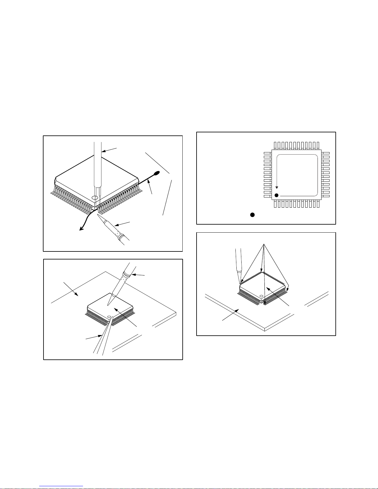
1. Removal
With Hot-Air Flat Pack-IC Desoldering Machine:
(1) Prepare the hot-air flat pack-IC desoldering ma-
chine, then apply hot air to the Flat Pack-IC (about 5
to 6 seconds). (Fig. S-1-1)
Fig. S-1-1
(2) Remove the flat pack-IC with tweezers while apply-
ing the hot air.
(3) Bottom of the flat pack-IC is fixed with glue to the
CBA; when removing entire flat pack-IC, first apply
soldering iron to center of the flat pack-IC and heat
up. Then remove (glue will be melted). (Fig. S-1-6)
(4) Release the flat pack-IC from the CBA using twee-
zers. (Fig. S-1-6)
Caution:
1. Do not supply hot air to the chip parts around the flat
pack-IC for over 6 seconds because damage to the
chip parts may occur. Put masking tape around the
flat pack-IC to protect other parts from damage.
(Fig. S-1-2)
2. The flat pack-IC on the CBA is affixed with glue, so
be careful not to break or damage the foil of each pin
or the solder lands under the IC when removing it.
Hot-air
Flat Pack-IC
Desoldering
Machine
CBA
Flat Pack-IC
Tweezers
Masking
Tape
Fig. S-1-2
(1) Using desoldering braid, remove the solder from all
pins of the flat pack-IC. When you use solder flux
which is applied to all pins of the flat pack-IC, you can
remove it easily. (Fig. S-1-3)
Flat Pack-IC Desoldering Braid
Soldering Iron
Fig. S-1-3
(2) Lift each lead of the flat pack-IC upward one by one,
using a sharp pin or wire to which solder will not
adhere (iron wire). When heating the pins, use a fine
tip soldering iron or a hot air desoldering machine.
(Fig. S-1-4)
Fine Tip
Soldering Iron
Sharp
Pin
Fig. S-1-4
(3) Bottom of the flat pack-IC is fixed with glue to the
CBA; when removing entire flat pack-IC, first apply
soldering iron to center of the flat pack-IC and heat
up. Then remove (glue will be melted). (Fig. S-1-6)
(4) Release the flat pack-IC from the CBA using twee-
zers. (Fig. S-1-6)
With Iron Wire:
(1) Using desoldering braid, remove the solder from all
pins of the flat pack-IC. When you use solder flux
which is applied to all pins of the flat pack-IC, you can
remove it easily. (Fig. S-1-3)
(2) Affix the wire to a workbench or solid mounting point,
as shown in Fig. S-1-5.
(3) While heating the pins using a fine tip soldering iron
or hot air blower, pull up the wire as the solder melts
so as to lift the IC leads from the CBA contact pads
as shown in Fig. S-1-5.

DV-SL700W
6
How to Remove / Install Flat Pack-IC
1. Removal
With Hot-Air Flat Pack-IC Desoldering Machine:
(1) Prepare the hot-air flat pack-IC desoldering ma-
chine, then apply hot air to the Flat Pack-IC (about 5
to 6 seconds). (Fig. S-1-1)
Fig. S-1-1
(2) Remove the flat pack-IC with tweezers while apply-
ing the hot air.
(3) Bottom of the flat pack-IC is fixed with glue to the
CBA; when removing entire flat pack-IC, first apply
soldering iron to center of the flat pack-IC and heat
up. Then remove (glue will be melted). (Fig. S-1-6)
(4) Release the flat pack-IC from the CBA using twee-
zers. (Fig. S-1-6)
Caution:
1. Do not supply hot air to the chip parts around the flat
pack-IC for over 6 seconds because damage to the
chip parts may occur. Put masking tape around the
flat pack-IC to protect other parts from damage.
(Fig. S-1-2)
2. The flat pack-IC on the CBA is affixed with glue, so
be careful not to break or damage the foil of each pin
or the solder lands under the IC when removing it.
Hot-air
Flat Pack-IC
Desoldering
Machine
CBA
With Soldering Iron:
(1) Using desoldering braid, remove the solder from all
pins of the flat pack-IC. When you use solder flux
which is applied to all pins of the flat pack-IC, you can
remove it easily. (Fig. S-1-3)
Flat Pack-IC Desoldering Braid
Soldering Iron
Fig. S-1-3
(2) Lift each lead of the flat pack-IC upward one by one,
using a sharp pin or wire to which solder will not
adhere (iron wire). When heating the pins, use a fine
tip soldering iron or a hot air desoldering machine.
(Fig. S-1-4)
Fine Tip
Soldering Iron
Sharp
Pin
Fig. S-1-4
(3) Bottom of the flat pack-IC is fixed with glue to the
CBA; when removing entire flat pack-IC, first apply
soldering iron to center of the flat pack-IC and heat
up. Then remove (glue will be melted). (Fig. S-1-6)
(4) Release the flat pack-IC from the CBA using twee-
zers. (Fig. S-1-6)
With Iron Wire:
(1) Using desoldering braid, remove the solder from all
pins of the flat pack-IC. When you use solder flux
which is a
pp
lied to all
p
ins of the flat
p
ack-IC
,y
ou can
(4) Bottom of the flat pack-IC is fixed with glue to the
CBA; when removing entire flat pack-IC, first apply
soldering iron to center of the flat pack-IC and heat
up. Then remove (glue will be melted). (Fig. S-1-6)
(5) Release the flat pack-IC from the CBA using twee-
zers. (Fig. S-1-6)
Note:
When using a soldering iron, care must be taken to
ensure that the flat pack-IC is not being held by glue.
When the flat pack-IC is removed from the CBA,
handle it gently because it may be damaged if force
is applied.
To Solid
Mounting Point
Soldering Iron
Iron Wire
or
Hot Air Blower
Fig. S-1-5
Fine Tip
Soldeing Iron
CBA
Flat Pack-IC
Tweezers
Fig. S-1-6
2. Installation
(1) Using desoldering braid, remove the solder from the
foil of each pin of the flat pack-IC on the CBA so you
can install a replacement flat pack-IC more easily.
(2) The "●" mark on the flat pack-IC indicates pin 1. (See
Fig. S-1-7.) Be sure this mark matches the 1 on the
PCB when positioning for installation. Then presol-
der the four corners of the flat pack-IC. (See Fig. S-
1-8.)
(3) Solder all pins of the flat pack-IC. Be sure that none
of the pins have solder bridges.
Example :
Pin 1 of the Flat Pack-IC
is indicated by a " " mark. Fig. S-1-7
Presolder
CBA
Flat Pack-IC
Fig. S-1-8

DV-SL700W
7
(4) Bottom of the flat pack-IC is fixed with glue to the
CBA; when removing entire flat pack-IC, first apply
soldering iron to center of the flat pack-IC and heat
up. Then remove (glue will be melted). (Fig. S-1-6)
(5) Release the flat pack-IC from the CBA using twee-
zers. (Fig. S-1-6)
Note:
When using a soldering iron, care must be taken to
ensure that the flat pack-IC is not being held by glue.
When the flat pack-IC is removed from the CBA,
handle it gently because it may be damaged if force
is applied.
To Solid
Mounting Point
Soldering Iron
Iron Wire
or
Hot Air Blower
Fig. S-1-5
Fine Tip
Soldeing Iron
CBA
Flat Pack-IC
Tweezers
Fig. S-1-6
2. Installation
(1) Using desoldering braid, remove the solder from the
foil of each pin of the flat pack-IC on the CBA so you
can install a replacement flat pack-IC more easily.
(2) The "●" mark on the flat pack-IC indicates pin 1. (See
Fig. S-1-7.) Be sure this mark matches the 1 on the
PCB when positioning for installation. Then presol-
der the four corners of the flat pack-IC. (See Fig. S-
1-8.)
(3) Solder all pins of the flat pack-IC. Be sure that none
of the pins have solder bridges.
Example :
Pin 1 of the Flat Pack-IC
is indicated by a " " mark. Fig. S-1-7
Presolder
CBA
Flat Pack-IC
Fig. S-1-8
Instructions for Handling
Semi-conductors
Electrostatic breakdown of the semi-conductors may
occur due to a potential difference caused by electrostatic
charge during unpacking or repair work.
1. Ground for Human Body
Be sure to wear a grounding band (1MΩ) that is properly
grounded to remove any static electricity that may be
charged on the body.
2. Ground for Workbench
Be sure to place a conductive sheet or copper plate with
proper grounding (1MΩ) on the workbench or other
surface, where the semi-conductors are to be placed.
Because the static electricity charge on clothing will not
escape through the body grounding band, be careful to
avoid contacting semi-conductors with your clothing.
CBA
< Incorrect >
CBA
Grounding Band
Conductive Sheet or
Copper Plate
< Correct >

DV-SL700W
8
OPERATING CONTROLS AND FUNCTIONS
nMain unit (front panel)
1. Disc Tray
2. STANDBY Indicator
3. PLAY/PAUSE Indicator
4. Remote Sensor
5. Disc Tray OPEN/CLOSE Button
6. Play or Pause Button
7. STOP Button
8. ON/STANDBY
nMain unit (rear panel)
1. AC Cord Lead
2. Component Video Output Sockets
3. Video Output Socket
4. Digital Output Socket(Coaxial)
5. Audio Output Sockets
6. S-Video Output Socket
12
345678
123
6
5
4

DV-SL700W
9
nRemote control
1. Remote Control Transmitter
2. MENU/PBC Button
3. Disc Tray Open/ Close Button
4. Title Select Button
5. Fast Backward/Chapter (track) skip down
6. Fast Forward/Chapter (track) skip up
7. Direct Number Buttons
8. PROGRAM / ANGLE Button
9. MUTE Button
10. ON/STANDBY Button
11. SETUP/GO TO Button
12. SLOW Button
13. STOP Button
14. ENTER / PLAY / PAUSE Button
15. Cursor Up and Down Buttons
16. Subtitle Select Button
17. Audio Select Button
18. Repeat A - B Button
19. Repeat Play Button
20. ZOOM Button
21. DISPLAY Button
1
2
3
4
5
6
7
8
9
10
11
12
13
14
15
16
17
18
19
20
21

DV-SL700W
10
BLOCK DIAGRAMS
Figure 1: BLOCK DIAGRAM
O/P
4558
FLASH
MX29LV040T
C-70
SUNPLUS
SHPE8202D
SDRAM
512X16X2
RESET
CM3403-29SO
MOTOR
AM5869
LOADER
POWER
AC~110-240V
EEPROM
AF24BC02
IR LED
L-OUT
L-OUT
R-OUT R-OUT
VIDEO OUT
SVIDEO OUT
Y
Pb
Pr
COAXIAL
KEY
8550SS
M07S
STANDBY
P+5V
GND
P+12V
+3.3V +1.8V
8550SS
VIDEO OUT
S-VIDEO OUT
Y.U.V
SPDIF OUT
AUDIO OUT

DV-SL700W
11
SCHEMATIC DIAGRAMS
CONTROL PCB SCHEMATIC
Figure 1: CONTROL PCB SCHEMATIC
DATA
CS
CLK
R206
10
D204
1N4148
D203
1N4148
1
2
3
4
5
6
7
8
RB201
IR/VFD
LED2
R205
10K
R207
10K
IR
GND
VCC
LED3
Q302
2SA733
Q301
2SA733
R203
1K R204
1K
R201
560
R202
560
D202
RED LED
D201
GREEN LED
R209
4.7K R208
4.7K
SN201
IRT
TA201
EJECT
TA202
ON/STD BY
TA203
PLAY/PAUSE
TA204
STOP
+
C14
100uF/16V
C12
104 D101
1N4148
D102
1N4148
D103
1N4148
D104
1N4148
D105
1N4148
+
C13
330uF/10V
63PIN
62PIN
A
B
C
D
E
F
G
H
123456

DV-SL700W
12
MAIN PCB SCHEMATIC
Figure 2: MAIN PCB SCHEMATIC (1/8)
D
CD_VR
LDSW
DVD_VR
CD_VR
PUH_CDLD
DVD_VR
PUH_DVDLD
CDMDI
B
CDVR
PUH_CDLD#
PUH_DVDLD#
C
A
PUHRF
E
F
DVD_VR#
DVDMDI
VREF1
PUH_DVDLD
DVDLDO
CDLDO
PUH_CDLD
C119
0.1UF
+C181
47UF16V
R154
5.1
+C180
47UF16V
+C176
100UF10V
R155
5.1
C118
0.1UF
C120
0.1UF
R146
0
R145 0
L11 10UH
C102
0.1UF
R157
100K
C101
0.1UF
R159
470
C104
0.1UF
R156 100K
C103
0.1UF
R158
470
C179 0.1U
26 25
17
16
15
14
13
12
11
10
9
8
7
6
5
4
3
2
1
18
19
20
21
22
23
24
27 28
CN101
ELCO-CON24(Left)
R144 0
C107
0.1UF
R143 0
C106
0.1UF
C10
8
0.1U
F
C178
0.1U
C105
0.1UF
C177 0.1U
TP4
FOC-
TP3
FOC+
TP2
RAD-
L12 10UH
TP1
RAD+
GND
GND
RF+5V
GND
GND
RF+5V
GND
DVCC33 VCC1.8
P
L
RF+5V
GND GND
G
GND
RF3.3V
GND
RF3.3V
BOTTOM CONTACT
FORVHWR FRQQHFWRU
Pickup head parameter Motor Driver AT5660
5.1
4.7
1000P
Motor Driver AM5668
39K
00
R63
1000P
R53 C32
2.2K
20K
R15R40
Sanyo
39K4.7
R14
1000P
R62
100 2700P
20K
C33
1000P
33K
Sony
68K 1000P
100 3.3K
5.1
R39 R62 C32 R63 C33
1000P1500P 68K12K
Samsung
Mitsumi
5.1
5.1
5.1
5.1
0
0
0
0
2.2K
2.2K
12K
12K
1500P
1500P
68K
68K
1000P
1000P
39K
39K
3.3K
3.3K
2700P
2700P
1000P
1000P
FOC-
FOC+
RAD+
RAD-
FOC+
FCO
FOC-
VOFC+ 14
VOFC- 13
RFGO1
5
RFGO3
3
TRB1
2
VINFC
1
BIAS
25K
+
-
-
Actuator
10K
Driver(6 x)
+
-
IC105
AM5869S
DIP28-SSOPH
REGO3
TRB1
RFGO1
Q105
3904
G
D S
Q103
2SK3018
G
DS
Q104
2SK3018
GND
Q101
2SB1132
Q102
2SB1132
D102
1N4148
D101
1N4148
A
B
C
D
E
F
G
H
123456

DV-SL700W
13
MAIN PCB SCHEMATIC
Figure 2: MAIN PCB SCHEMATIC (2/8)
AU_XCK
V_H_SYNC
AU_BCK
RA16
V_V_SYNC
RA18
SPDIF_OUT
AU_D0
AU_D1
AU_D2
AU_LRCK
AUDIO_MUTE
RFI
RFO
V_COMP
V_BIAS
CVBS1
V_FSADJ
V_REF
B/U
G/Y
R/V
Vref0
FD
LGIN
PD
XOPVIN1
XOPOP1
XOPVIP1
TEO
RFCT
SBAD
FEO
DVDMDI
CDLDO
DVDLDO
CDMDI
VREF1
F
CDA
CDB
E
PUHRF
RFIP
DPDC
A
B
C
D
DPDA
RFRP
DAC_REF
DA R
TP11
RFIP
C110
0.1UF
R114
150K
C160
0.01UF
R164 1.2K (1%)
AGCOP
2
RFIP
3
RFIS
4
RFSUM
5
DPDA
6
DPDB
7
DPDC
8
DPDD
9
DVDD
10
DVDC
11
DVDB
12
DVDA
13
CDB
14
CDA
15
CDF
16
CDE
17
RF_AVSS
18
APC_AVSS
19
DVDLDO
20
CDLDO
21
DVDMDI
22
APC_SRV_AVDD
24
V21
25
R33K
26
V165
27
SVOTST
28
RFRPPH
29
RFRPBH
30
RFRPMEAN
31
SBADPH
32
SBAD
33
FEO
34
TEO
35
TEOLP
36
OPVIP
37
OPVIN
38
OPVOP
39
SRV AD AVSS VRGD
40
AGCON
1
FLTIN 216
FLTIP 215
RFO 214
AGCCAP 212
GMRES 211
RF_AVDD 210
DS_AVDD 209
SLVL 208
CNIN 207
RFI 206
PLL_DS_AVSS 205
LGIN 204
LPFNIN 203
FDFLT 202
PDFLT 201
VREFO 200
LPFN 199
LPFO 198
PLL_AVDD 197
VSS_TVA2 196
TV_DAC5 195
VDD_TVA2 194
TV_DAC4 193
TV_DAC3 192
VSS_TVA1 191
VDD_TVA1 190
VSS_TVA0 189
VDD_TVA0 188
TV_DAC0 187
V_REFOUT 186
V_FSADJ 185
V_BIAS 184
V_COMP 183
UA0_TX/GPIO 182
UA0_RX/GPIO 181
A_XCK/GPIO 180
A_BCK/GPIO 179
VSS_K6/VSS_O6 178
A_LRCK/GPIO 177
A_DATA3/GPIO 176
A_DATA2/GPIO 175
A_DATA1/GPIO 174
VDD_O5 173
A_DATA0/GPIO 172
A_IEC_TX/GPIO 171
R_A18 170
R_A16 169
DAC_VSS 168
DAC_VDD 167
DA R 166
CDMDI
23
RFRP 213
IC101
SPHE8202S(D)-216PIN
C157 680PF
C123 0.1UF
C188 0.22UF
1
6V
R163 33K (1%)
C162 0.01UF
C161 0.01UF
1
46
C167 0.068UF
C213 330PF
R160 NG
107
1UF
C108
0.1UF
+
C153
10UF16V
TP5RFCT C186 0.047UF
C154 680PF
C210 0.1U
C168 100PF
TP9
CDA
R110 20K
TP8CDB
TP7F
C159 0.01UF
R112 5.1KR109 1.5K
C170 47PF
C163 1UF C169 47PF
R113 5.1K
C111
0.1UF
TP6E
C122 0.1UF
+C183
47UF16V
+
C182 47UF16V
C121
0.1UF
C166 1UF
C165 1UF
C184 300PF
C187 820PF
C109
0.1UF
TP24
RFRP
C155 680PF
C158 680PF
C156 680PF
C114
0.1UF
C112
0.1UF
C164
1UF
C113
0.1UF
C185 NC(120PF)
GND
GND DVCC33
GND
GND
PLL3.3V
RF3.3V
RF3.3V
GND
PLL3.3V
GND
VVCC3
VGND
GND
DVC
C
PLL3.3V
GND
GND
VVCC3
VGND
GND
GND
GND
GND
GND
GND
RF3.3V
GND
GND
GND
TV3
Y
CVB
(S-Video)
C
TV0
CVB
CVB
TV4
Y
B
TV
Cb
(S-Video)
C
G
R
CVB
TCO
VREF2
78 9 10 11 12

DV-SL700W
14
MAIN PCB SCHEMATIC
Figure 2: MAIN PCB SCHEMATIC (3/8)
PIN_142
PIN_141
PIN_125
AU_XCK
V_H_SYNC
AU_BCK
RA16
V_V_SYNC
RA18
SPDIF_OUT
AU_D0
AU_D1
AU_D2
AU_LRCK
AUDIO_MUTE
RA12
RA7
MA0
DQM0
DQM1
MA10
RA6
RA5
RA4
RA3
RA2
RA15
RA1
MA1
RA0
MA2
MA3
RD0
RD1
RD2
RD3
DQM2
DQM3
RD4
RD5
RD6
RD7
ROE
V_COMP
RA10
RA11
RA9
RA8
RA13
RA14
RA17
RWE
DA_R
DAC_REF
DA_L
R_A12 162
R_A7 161
R_A6 160
R_A5 159
R_A4 158
R_A3 157
R_A2 156
R_A1 155
R_A0 154
R_D0 153
R_D1 152
R_D2 151
VSS_O5/VSS_K5 150
R_D3 149
R_D4 148
R_D5 147
R_D6 146
R_D7 145
R_OE_B 144
VDD_K4 143
M_DQM2/GPIO 142
M_DQM3/GPIO 141
R_A10 140
R_A11 139
R_A9 138
R_A8 137
VDD_O4 136
R_A13 135
R_A14 134
R_A17 133
R_WE_B 132
M_A3 131
M_A2 130
M_A1 129
VSS_O4/VSS_K4 128
M_A0 127
M_A10 126
M_BA1/GPIO 125
M_DQM0/GPIO 124
M DQM1/GPIO 123
122
_
V_COMP
183
UA0_TX/GPIO 182
UA0_RX/GPIO 181
A_XCK/GPIO 180
A_BCK/GPIO 179
VSS_K6/VSS_O6 178
A_LRCK/GPIO 177
A_DATA3/GPIO 176
A_DATA2/GPIO 175
A_DATA1/GPIO 174
VDD_O5 173
A_DATA0/GPIO 172
A_IEC_TX/GPIO 171
R_A18 170
R_A16 169
DAC_VSS 168
DAC_VDD 167
DAC_REF 164
DA_R 166
DA_L 165
R_A15 163
GND DVCC33
GND
GND
DVCC33
VCC1.8
DVCC33
GND
RA16 A16
1
2
C171 NC
C116
0.1UF
C117
0.1UF
R137
390
C115 0.1UF
VVCC3
VVCC3
VGND
VGND
VGND
1/2 current config
TV3
Y
d
eo)
C
TV4
Y
B
TV5
Cb
(S-Video)
Cr
GR
CVB
R1
L1
R404 2.4K
R402 12K
R431 3K
C409
181
C424
562
C423
562
R429
1.5K
C403
10UF
C413 1
0
R403
2.4K
R401 12K
R430 3K
C408
180
C425
562
C422
562
R428
1.5K
C401
10UF
SDIN
1
DEM/SCLK
2
LRCK
3
MCLK
4
VQ
5FILT+ 6
AOUTL 7
AGND 8
VA 9
AOUTR 10
IC401
CS4344(NC)
6
5
2
3
R406 1
0
R405 10K
C174
10UF
C194
104
C173
10UF
C191
104
R140
33
VCC
AU_LRCK
AU_BCK
AU_D0
AU_XCK
C412
104
C196
100UF
C195
104
C416
100UF
C414
104
Q405
2N3906
R4
3
47k
R42310K
R418
1K
R432
6.8K
R419
1K
C421
220UF/16V
D404
1N4001
C427
220UF
LMUTE
Q404
2N3906
vccvcc
R42
0
1K
+12V vcc
Q403
2N3906
R417
1K
R421
1K
R416
2K
vcc
POWER NO
AUDIO MUTE
R138 NC(0)
R139 NC(0)
R
1
0
SPDIF_OUT
R302
75 OHM
R303
75 OHM
R301
75 OHM
R304
75 O
H
V
V
V
VCC
VCC
VCC
VCC VGND
VGND
VGND
VGND
VGND
VGNDVGND
VGND
ZD301
6.8V
ZD304
6.8V
ZD306
6.8V
ZD307
6.8V
ZD303
6.8V
ZD302
6.8V
ZD308
6.8V
ZD305
6.8V
18
27
36
45
RB101
33
18
27
36
45
RB102
33
V_BIAS
V_COMP
V_REF
V_FSADJ
18
27
36
45
RB106
33
18
27
36
45
RB107
33
18
27
36
45
RB105
33
R136 NC
R135 NC R-OUT
L-OUT
AUDIO_MUTE
XCK
14
LRCK
1
DIN
2
BCK
3
TST
4
VCM
5
GND
7VCC 8
AR 6
AL 9
DEM 12
FMT 13
IC401B
CF2752(NC)
R134
4.7K
ៜ㝍
⿌㝍
Ȳǵⵦ㝍
⠻㝍
A
B
C
D
E
F
G
H
123456

DV-SL700W
15
MAIN PCB SCHEMATIC
Figure 2: MAIN PCB SCHEMATIC (4/8)
140 132
IC103A
+12V
4
K
K
C409
181
4
13 104
4
K
K
C408
180
C402
10UF
C405
10UF
LMUTE
6
7
5
8
IC402B
NJM4558
2
1
4
3
IC402A
NJM4558
Q407
2N3906
R439
3K
R406 10K10K C404
100UF
C426
104
R408 1k
R411 1k
R434
10OHM
Q402
2N3904
Q401
2N3904
R437
470
R438
470
R410 1k
R412 1k C411
101
C410
101
1 2
FB402 601
1 2
FB401 601
4
12
1
04
R407 1k
R413 1k
LO
RO
C
416
0
0UF
4
14
1
04
R433
47k
2
7
U
FQ406
2N3906
R420
1K
vcc
POWER OFF
C309
15PF
R305
100
R307
10K
Q305
C945 R309
200
R308
1K
R306
100
VCC
SPDIF_OUT
3
4
5
6
7
8
1
2
9
JK101
RCA4
C313
101
C312
101
C311
101
C310
101
1 2
FB307 101
1 2
FB301 101
1 2
FB302 101
1 2
FB303 101
VGND
1
2
3
4
5
6
7
8
JK102
RCA+SVIDEO
VGND
YY
CC
C315
15PF C316
15PF
C314
15PF
CVB1_O-1
R/V_O
B/U_O
G/Y_O
1 2
FB304
101
1 2
FB305
101
1 2
FB306
101
L301
2.4UH
C305
470PF
R302
75 OHM
C301
470PF
L302 2.4UH
R303
75 OHM
C306
470PF
C302
470PF
L303 2.4UH
M
C307
470PF
C303
470PF
L304
2.4UH
R304
75 OHM
C308
470PF
C304
470PF
VGND
VGND
VGNDVGND
VGNDVGND
VGNDVGND
V
GND
VGND
V
GND
V
GND
RIN
1
2
LIN
3
AGND 4
GND
5
6
7
JK103
SC-R IN
SC-L IN
BIN
BIN
GIN
RIN
CVBS IN
R409 NC
R414 NC
R-OUT
L-OUT
SC-R IN
SC-L IN
R/V_O
G/Y_O
Q308
2N3904
R312
4.7K
R313
75
VCC
Q307
2N3904
ZD309
6.8V
R310
1K
+12V
R311
4.7K
SC8
SC16
SC1
SC2 1
2
3
4
CN401
NC
+12V
R-OUT
L-OUT
1 2
FB403 NC
1 2
FB405 NC
C432
NC
C431
NC
1 2
FB404 NC
C430
NC
1 2
FB309 101
1 2
FB308 101
SC-L IN
78 9 10 11 12

DV-SL700W
16
MAIN PCB SCHEMATIC
Figure 2: MAIN PCB SCHEMATIC (5/8)
TRAYIN
TRAYOUT
DVDLDO
R173 4.7K
R174 4.7K
R17
1
4.7K
XT1
27M
H
C199
33PF
C127
GND
GND
GND
VCC
GND
GND GND
FORVHWR FRQQHFWRU
C936
100UF16V
C904
0.1UF
FB910
FB
C905
0.1UF
R905
2.2
C921
104
C925
104
C901
0.1UF
1
2
3
5
6
7
4
CN901
POWER
GND
RF+5VM+5V
GND
SPDCO
LOAD-TRAY+
TRAY-
VREF2
SLED+
SLED-
RAD+
FOC+
DMEA
FCO
TCO
SLED-
SP+
SP-
SLED+
SCO
LOAD-
LOAD+
LOAD+
SP-
SP+
RAD-
FOC-
SP+SNSR
C126
0.1UF
C198
100UF16V
R115
150K
R170
1
AT5660
VOSL+ 17
VOSL- 18
VOSP- 12
VOSP+ 11
VOTK- 16
REGO2 20
VOTK+ 15
VINSL
23
Vcc1
8
VOLD+ 10
Vcc2
19
PreGND
22
STBY 28
VOFC+ 14
VOFC- 13
VINSP
4
RFGO1 5
TRB3
25
BIAS
27
VINTK
26
RFGO3
3
TRB1
2
VINFC
1
TRB2
24
VCTL
21
GND1
29
GND2
30
REV
7
FWD
6VOLD- 9
BIAS
25K
+
-
BIAS
-
+
-
+
DRIVER
TRAY
Pre-DRV
Actuator
Driver(4 x)
Actuator
Driver(4 x)
25K
10K
BIAS
Actuator
Driver(6 x)
Actuator
-
+
15K
10K
BIAS
-
+
10K
+
-
BIAS
-
+
15K
10K
10K
Driver(6 x)
+
-
-
+
25K
10K
IC105
AM5869S
DIP28-SSOPH
1
2
3
4
5
6
CN102
JST-CON6-2 mm
C125
0.1UF
C124
0.1UF
1
2
3
4
5
CN103
M+5V
GND
M+5V
GND
GND
GND
GND
REGO3
TRB1
RFGO1
TRB3
HOME
VCC
P+5V
GND
P+12V
SANDBY
P-27V
PAC1
PAC2
FB120 601
FB121 601
FB123 601
FB124 601
FB125 601
FB126 601
FB128 601
FB129 601
FB907 601
FB901 601/2A
FB902 601
FB903 601
FB904 601
FB905 601
FB127 601
C201
33PF
C20233PF
C203
33PF
C204
33PF
C205
33PF
C206
33PF
C207
33PF
C208
33PF
C209
33PF
C926
104
C927
104
C929
104
C930
104
C931
104
C932
104
VCC
+12V
-27V
AC1
AC2
C934
100UF16V
C923
104
D102
1N4148
D101
1N4148
S-BY
R147
0
R148
0
R166 0
R149 NC
R167 0
R150 NC
A
B
C
D
E
F
G
H
123456

DV-SL700W
17
MAIN PCB SCHEMATIC
Figure 2: MAIN PCB SCHEMATIC (6/8)
TRAYOUT
LDSW
LED3
P1
LED2
DFCT
MS_CLK
MS_BS
I2C_DATA
RESET_B
R_CS1
CARD_WP
CARD_SENSE2
VFD_DATA
VFD_CLK
VFD_STB
IR_IN
CLKOUT
CLKIN
CLKOUT
CLKIN
USB_DM
FGIN
RESET_B
USB_DP
I2C_CLK
RA19
MD3
MD4
MD0
MD7
MD6
MD2
MD5
MD1
M_BA0
M_CS0
MD14
MD11
M_RAS
MWE
MD15
MD13
MD12
M_CAS
MD10
TRAYIN
XOPVIN1
XOPOP1
XOPVIP1
TEO
RFCT
SBAD
FEO
DVDMDI
CDLDO
DVDLDO
CDMDI
VREF1
F
E
CDF
16
CDE
17
RF_AVSS
18
APC_AVSS
19
DVDLDO
20
CDLDO
21
DVDMDI
22
APC_SRV_AVDD
24
V21
25
R33K
26
V165
27
SVOTST
28
RFRPPH
29
RFRPBH
30
RFRPMEAN
31
SBADPH
32
SBAD
33
FEO
34
TEO
35
TEOLP
36
OPVIP
37
OPVIN
38
OPVOP
39
SRV_AD_AVSS_VRGD
40
AD_DA_AVDD
41
DATEO
42
DAFEO
43
DA_AVSS
44
TRAY_IS_IN
45
TRAY_IS_OUT
46
SPDC_OUT/GPIO
47
SC_OUT/GPIO
48
SC1_OUT/GPIO
49
TRAY_OUT/GPIO
50
DMEA/GPIO
51
FGIN/GPIO
52
HOMESW/GPIO
53
LDSW/GPIO
54
DFCT/GPIO
55
VDD_K1
56
GPIO/SD_CK/MS_CK
57
GPIO/SD_CMD/MS_BS
58
GPIO/ttio0_4/SD_D0/MS_D0
59
VSS_O1/VSS_K1
60
GPIO/ttio1_5/SD_D1/MS_D1
61
GPIO/ttio2_6/SD_D2/MS_D2
62
GPIO/ttio3_7/SD_D3/MS_D3
63
VDD_O1
64
GPIO
65
R_CS4_B/GPIO
66
R_CS3_B/GPIO
67
R_CS2_B/GPIO
68
R_CS1_B/GPIO
69
RST_B
70
IR_IN/GPIO
71
VFD_CLK/GPIO
72
VFD_STB/GPIO
73
VFD_DATA/GPIO
74
R_20/E_MX10
75
R_A19
76
CLKIN
77
CLKOUT
78
USB_GND
79
USB_VDD
80
USB_DP
81
USB_DM
82
VSS_PLLA
83
VDD_PLLA
84
VSS_PLLV
85
VDD_PLLV
86
M_D7
87
M_D6
88
M_D5
89
M_D4
90
M_D3
91
VDD_O2
92
M_D2
93
M_D1
94
M_D0
95
M_WE_B
96
M_CAS_B
97
M_RAS_B
98
VSS_O2/VSS_K2
99
M_CS0_B/GPIO
100
M_BA0
101
M_D15
102
M_D14
103
M_D13
104
VDD_K2
105
M_D12
106
M_D11
107
MD10
108
V
V
CDMDI
23 IC101
SPHE8202S(D)-216PIN
C188 0.22UF
C212 1000PF
TP10FGIN
R163 33K (1%)
R175 68K
C162 0.01UF
C161 0.01UF
R111 33K
C211 1000PF
C213 330PF
R160 NG
R171
4.7K
XT1
27MHz
C200
33PF
C199
33PF
TP5RFCT C186 0.047UF
C210 0.1U
TP7F
R176 2.2K
R177 2.2K
C127 0.1UF
R172 4.7K
C128 0.1UF
TP6E
C122 0.1UF
+C183
47UF16V
+
C182 47UF16V
C121
0.1UF
C184 300PF
C187 820PF
R151
0
GND
D
VCC
GND
VCC1.8
GND
GND
GND
GND
APLLVCC3
VPLLVCC1.8
GND
RF3.3V
GND
DVCC33 VCC1.8
GND
DVCC33
RF3.3V
GND
GND
GND
GND
RF3.3V
GND
GND
GND
USB_DP
USB_DM
R142
1K
R141
1K
A0
1
A1
2
A2
3
GND
4SDA 5
SCL 6
WP 7
VCC 8
IC104
24C01/CAT24C021
C129 0.1UF
GND
GND
VCC
I2C ADDR = 0XA0
FB918
FB
C913
0.1UF
+
C916
100UF16V
C907
0.1UF +C919
100UF16V
C912
0.1UF
C908
0.1UF
R103
33
C920
104
C938
220UF16V
C130
0.1UF
C905
0.1UF
R905
2.2
R9062.2
FB913 FB
R908
10
C911
0.1UF
FB912
FB
G
ND
RF+5V
PLL3.3V
VPLLVCC1.8
GND
VVCC3
SD_VCC3
GND
GND
GND
GND
RF3.3V
VGND
T30
Reset
DVCC33
R178
100K
C216
104
C219
103
IC120
LM809
C217
104
DVCC33
P
+
VREF2
XOPVIN1 XOPOP1
XOPVIP1
R115
150K
R170
1
R161
470K
C214
4700PF
R116
150K R162
470K
C215
4700PF
DVCC33
R902
12K
Q901
2SCS8550D(1.5A;1W)
C9390.1uF
R904
4.7K
C940
0.1uF
Q902
2SS8550D(1.5A;1W)
R903
10K
R901
20K
R909
1.2R/0.5W
R907
3.3R/0.5W
D902
1N5401
+
C942100uF
+
C941100uF
VCC
REGO3
TRB1
RFGO1
TRB3
TCO
FCO
SPDCO
SCO
TRAY-
TRAY+
DMEA
HOME
VREF2
V
CC
VCC
SC1
SC2
VCC1.8
S-BY
FB137
601
78 9 10 11 12

DV-SL700W
18
MAIN PCB SCHEMATIC
Figure 2: MAIN PCB SCHEMATIC (7/8)
PIN_142
PIN_141
PIN_125
MA9
MA7
MA6
MA5
MD9
CKE
MA8
MD8
MA4
MA0
DQM0
DQM1
MA10
MA11
MA1
MA2
MA3
DQM2
DQM3
RD6
RD7
ROE
MD3
MD4
MD0
MD2
MD5
RA10
MD1
RA11
M_BA0
M_CS0
RA9
MD14
MD11
M_RAS
MWE
MD15
MD13
MD12
M_CAS
MD10
RA8
RA13
RA14
RA17
RWE
_
M_D5
89
M_D4
90
M_D3
91
VDD_O2
92
M_D2
93
M_D1
94
M_D0
95
M_WE_B
96
M_CAS_B
97
M_RAS_B
98
VSS_O2/VSS_K2
99
M_CS0_B/GPIO
100
M_BA0
101
M_D15
102
M_D14
103
M_D13
104
VDD_K2
105
M_D12
106
M_D11
107
M_D10
108
R_D
6146
R_D7 145
R_OE_B 144
VDD_K4 143
M_DQM2/GPIO 142
M_DQM3/GPIO 141
R_A10 140
R_A11 139
R_A9 138
R_A8 137
VDD_O4 136
R_A13 135
R_A14 134
R_A17 133
R_WE_B 132
M_A3 131
M_A2 130
M_A1 129
VSS_O4/VSS_K4 128
M_A0 127
M_A10 126
M_BA1/GPIO 125
M_DQM0/GPIO 124
M_DQM1/GPIO 123
M_A4 122
VDD_K3 121
M_A5 120
M_A6 119
M_A7 118
M_A8 117
M_A9 116
M_CKE/GPIO 115
VSS_O3/VVV_K3 114
M_CLKO 113
VDD_O3 112
M_A11/GPIO 111
M_D8 110
M_D9 109
GND
DVCC33
VCC1.8
GND
VCC1.8
GND
DVCC33
A
PLLVCC3
8
DVCC33 VCC1.8
SDRAM_CLK
MA1
MA2
MA4
MA5
MA6
MA7
MA9
RWE
MWE
DQM1
DQM0
RA9
RA13
RA8
RA11
RA1
RA2
RA3
RA7
RA15
RA12
RA5
RA4
RA6
RA14
CKE
MD9
MD10
MD8
M_BA0
RA18
MA3
MA8
MA10
MA0
MD6
MD7
MD4
MD5
MD13
MD14
MD12
MD15
MD11
M_CAS
M_RAS
M_CS0
D5
D6
D4
D7
D8
D9
D10
D11
D12
D13
D14
D15
RA16
RAM_CLK
MD2
MD3
D2
D0
MD1
MD0
D1
D3
R
1
R105 33
C220 10PF
VCC 1
DQ0 2
DQ1 3
VSSQ 4
DQ2 5
DQ3 6
VCCQ 7
DQ4 8
DQ5 9
VSSQ 10
DQ6 11
DQ7 12
VCCQ 13
DQML
14
WE
15 CAS
16 RAS
17 CS
18
BA/A11
19 A10
20
A0
21
A1
22
A2
23
A3
24
VCC 25
VSS
26
A4
27
A5
28
A6
29
A7
30
A8
31
A9
32
NC
33
CKE
34 CLK
35
DQMH
36
NC
37
VCCQ 38
DQ8 39
DQ9 40
VSSQ 41
DQ10 42
DQ11 43
VCCQ 44
DQ12 45
DQ13 46
VSSQ 47
DQ14 48
DQ15 49
VSS
50
IC106
SDRAM 16M-6(512Kx16x2)
C132
0.1UF
C133
0.1UF
C134
0.1UF
C135
0.1UF
C136
0.1UF
+
C152
100UF16V
SD_VCC3
GND
SD_VCC3
GND
GND
SD_VCC3
GND
GND
SDRAM_CLK
3
0
U
F
A16
1
A15
2
A14
3
A13
4
A12
5
A11
6
A9
7
A8
8
WE#
9
NC
10
NC
11
NC
12
A18
13
A7
14
A6
15
A5
16
A4
17
A3
18
A2
19
A1
20
IC103C
1 8
2 7
3 6
4 5
RB116
33
1 8
27
3 6
4 5
RB117
33
1 8
27
3 6
4 5
RB115
33
1 8
2 7
3 6
4 5
RB114
33
SDRAM_CLK
Q405
2N3906
R4
3
47k
10
K
R419
1K
C421
220UF/16V
C427
220UF
LMUTE
Q404
2N3906
1K
Q403
2N3906
R417
1K
POWER NO
AUDIO MUTE
1 8
2 7
3 6
4 5
RB110
33
18
27
36
45
RB111
33
A1
A2
A4
A5
A6
A7
A9
BA0
A3
A8
A10
A0
18
2
7
36
45
RB113
33
S-MWE
CAS
RAS
CS0
R107 33
R108 33M-DQM1
M-DQM0
18
27
36
45
RB106
33
18
27
36
45
RB107
33
R184 33
R185 33
R186 33
R187 33
18
27
36
45
RB105
33
AUDIO_MUTE
SD_VCC3
C221
0.1UF
C222
0.1UF
C224
0.1UF
C225
0.1UF
C23
9
0.1U
F
C237
0.1UF
C238
0.1UF
C236
0.1UF
C234
0.1UF
C235
0.1UF
C232
0.1UF
C230
0.1UF
C231
0.1UF
VGND AGND
VGND
A
B
C
D
E
F
G
H
123456

DV-SL700W
19
MAIN PCB SCHEMATIC
Figure 2: MAIN PCB SCHEMATIC (8/8)
R_CS1
ROE
RD7
RD4
RD6
RD3
RD5
RD0
RD2
RD1
RA10
RA17
RA0
MD9
MD10
MD8
RA19
RA18
MD6
MD7
MD4
MD5
MD13
MD14
MD12
MD15
MD11
FLASH_POWER
FLASH_POWER
DQM3
DQM2
RAM_CLK
D0
D1
D2
D3
D4
D5
D6
D7
D8
D9
D10
D11
D12
D13
D14
D15
MD2
MD3
MD1
MD0
VCC 1
DQ0 2
DQ1 3
VSSQ 4
DQ2 5
DQ3 6
VCCQ 7
DQ4 8
DQ5 9
VSSQ 10
DQ6 11
DQ7 12
VCCQ 13
DQML
14
WE
15 CAS
16 RAS
17 CS
18
BA/A11
19 A10
20
A0
21
A1
22
A2
23
A3
24
VCC 25
VSS
26
A4
27
A5
28
A6
29
A7
30
A8
31
A9
32
NC
33
CKE
34 CLK
35
DQMH
36
NC
37
VCCQ 38
DQ8 39
DQ9 40
VSSQ 41
DQ10 42
DQ11 43
VCCQ 44
DQ12 45
DQ13 46
VSSQ 47
DQ14 48
DQ15 49
VSS
50
IC107
NC
R153 0
C137
0.1UF
C136
0.1UF
GND GND
SD_VCC3
1
2
3
5
6
7
8
9
4
CN105
IR/VFD
C131
0.1UF
GND
A16
A15
A14
A13
A12
A11
A9
A8
WE#
NC
NC
NC
A18
A7
A6
A5
A4
A3
A2
A1 A0 21
CE# 22
GND 23
OE# 24
DQ0 25
DQ1 26
DQ2 27
DQ3 28
NC 29
VCC 30
VCC 31
DQ4 32
DQ5 33
DQ6 34
DQ7 35
A10 36
A19 37
NC 38
GND 39
A17 40
IC103CSST39LF080/016
SST
GND
A11
1
A9
2
A8
3
A13
4
A14
5
A17
6
WE
7
VCC
8
A18
9
A16
10
A15
11
A12
12
A7
13
A6
14
A5
15
A4
16 A3 17
A2 18
A1 19
A0 20
Q0 21
Q1 22
Q2 23
GND 24
Q3 25
Q4 26
Q5 27
Q6 28
Q7 29
CE 30
A10 31
OE 32
IC103A
MXIC 29LV040/SST39VF040
C218
104
RA0
RA4
RA1
RA2
RA3
RA5
RA8
RA6
RA9
RA11
RA12
RA15
RA10
RA7
RA14
RA13
RA17
RA16
ROE
RWE
R_CS1
RD3
RD4
RD5
RD1
RD0
RD2
RD7
RD6
FLASH_POWER
R433
47k
7
F
Q406
2N3906
R420
1K
POWER OFF
RIN
1
2
LIN
3
AGND 4
GND
5
6
BIN
7
AV CON 8
GND
9
10
GIN
11
12
GND
13
14
RIN
15
RGB CON 16
GND
17
GND 18
CVBS IN
19
20
GND
21
JK103
SCART OUT
SC-R IN
SC-L IN
BIN
GIN
RIN
CVBS IN
VGND VGND
IR
VFD-CLKO
VFD-DATA
VFD-CEO
VCC
GND
-27V
AC1
AC2
FB130 601
FB131 601
FB132 601
FB133 601
FB134 601
FB135 601
FB136 601
C145
101
C144101
C143
101
C142
101
C141
101
C140101
C139 104
C138101
A1
A2
A4
A5
A6
A7
A9
BA0
A3
A8
A10
A0
S-MWE
CAS
RAS
CS0
CKE
SC2
SC8
SC16
1
2
3
4
NC
+12V
R-OUT
L-OUT
1 2
1 2
FB405 NC
C432
NC
C431
NC
1 2
C430
NC
VFD_DATA
VFD_CLK
VFD_STB
IR_IN
LED2
LED3
C
C3
R104
4.7K
R101
4.7K
C223
0.1UF
C222
0.1UF
C226
0.1UF
C225
0.1UF
VCCC239
0.1UF
238
1UF
D
78 9 10 11 12

DV-SL700W
20
POWER PCB SCHEMATIC
Figure 3: POWER PCB SCHEMATIC (1/2)
T250V/1A
1N4007
0.1uF/250V
15uF/400V
C11
330uF/16V
470K
470K
470R
103/50V
472/50V
0.47UF/50V
2200PF/100
V
3300PF/250V
C6
C3
R9
1K
C5
R13
4.7K
560R
1N4148
1N5822
39K
820K
820K 100K 4700PF/1KV
0.001UF/100V
FR107
R2
R5 R5
D5
C2
C4
R6
R10
R8
D7
D14
C19
CY3
1
R
R7
R1
!
!
!
!
!
!
!
D2
5
4
2
4
3
2
7
7
8
8
1
1
4
88
5
D1
D3 D4
F1
C1
T1
10 10
11 11
12
12
LF1
CX1
CON1
Q1
R11
R12
220R
10K
Q2
Q5
ZD3
18V
PC1-2
03NK60
Ac Power
Supply Cord
AC 110 ~ 240 V
50/60Hz
R4
L
N
4.7R
4.7R
4.7R
4.7R
R14
R17
R16
PMBS3906
PMBS3904
A
B
C
D
E
F
G
H
123456
When servicing, pay attention as the area closed
by this line ( ) is directly connected with
AC.
Table of contents
Other Sharp DVD Player manuals

Sharp
Sharp DV-760S User manual

Sharp
Sharp DV-SL80U User manual

Sharp
Sharp DV-760X User manual

Sharp
Sharp DV-SL10S(G) User manual

Sharp
Sharp DV-SL1200W User manual

Sharp
Sharp DV-SV90S(Y) User manual

Sharp
Sharp DV-SL10X User manual

Sharp
Sharp DV-SV97S(RU) User manual

Sharp
Sharp DV-S1 User manual

Sharp
Sharp DV-SL80 User manual

Sharp
Sharp DV-SL85X User manual

Sharp
Sharp DV-SV97S(U) User manual

Sharp
Sharp QT-V5H User manual

Sharp
Sharp DV-SV80S User manual

Sharp
Sharp DV-600S User manual

Sharp
Sharp DV-620S User manual

Sharp
Sharp DV-SL80X User manual

Sharp
Sharp QT-V5E User manual

Sharp
Sharp DV-SV90S(B) User manual

Sharp
Sharp DV-S1U User manual